Paper Menu >>
Journal Menu >>
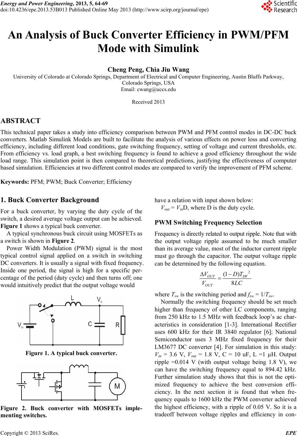 Energy and Power Engineering, 2013, 5, 64-69 doi:10.4236/epe.2013.53B013 Published Online May 2013 (http://www.scirp.org/journal/epe) An Analysis of Buck Converter Efficiency in PWM/PFM Mode with Simulink Cheng Peng, Chia Jiu Wang University of Colorado at Colorado Springs, Department of Electrical and Computer Engineering, Austin Bluffs Parkway, Colorado Springs, USA Email: cwang@uccs.edu Received 2013 ABSTRACT This technical paper takes a study into efficiency comparison between PWM and PFM control modes in DC-DC buck converters. Matlab Simulink Models are built to facilitate the analysis of various effects on power loss and converting efficiency, including different load conditions, gate switching frequency, setting of voltage and current thresholds, etc. From efficiency vs. load graph, a best switching frequency is found to achieve a good efficiency throughout the wide load range. This simulation point is then compared to theoretical predictions, justifying the effectiveness of computer based simulation. Efficiencies at two different control modes are compared to verify the improvement of PFM scheme. Keywords: PFM; PWM; Buck Converter; Efficiency 1. Buck Converter Background For a buck converter, by varying the duty cycle of the switch, a desired average voltage output can be achieved. Figure 1 shows a typical buck converter. A typical synchronous buck circuit using MOSFETs as a switch is shown in Figure 2. Power Width Modulation (PWM) signal is the most typical control signal applied on a switch in switching DC converters. It is usually a signal with fixed frequency. Inside one period, the signal is high for a specific per- centage of the period (duty cycle) and then turns off; one would intuitively predict that the output voltage would Figure 1. A typical buck converter. Figure 2. Buck converter with MOSFETs imple- have a relation with inpu menting switches. t shown below: PWM Switching Frequency Selection ote that with Vout = VinD, where D is the duty cycle. Frequency is directly related to output ripple. N the output voltage ripple assumed to be much smaller than its average value, most of the inductor current ripple must go through the capacitor. The output voltage ripple can be determined by the following equation. 2 (1 )VDT 8 OUT SW OUT VL C where Tsw is the switching period and fsw = 1/Tsw. t much hi Normally the switching frequency should be se gher than frequency of other LC components, ranging from 250 kHz to 1.5 MHz with feedback loop’s ac char- acteristics in consideration [1-3]. International Rectifier uses 600 kHz for their IR 3840 regulator [6]; National Semiconductor uses 3 MHz fixed frequency for their LM3677 DC converter [4]. For simulation in this study: Vin = 3.6 V, Vout = 1.8 V, C = 10 uF, L =1 µH. Output ripple =0.014 V (with output voltage being 1.8 V), we can have the switching frequency equal to 894.42 kHz. Further simulation study shows that this is not the opti- mized frequency to achieve the best conversion effi- ciency. In the next section it is found that when fre- quency equals to 1600 kHz the PWM converter achieved the highest efficiency, with a ripple of 0.05 V. So it is a tradeoff between voltage ripples and efficiency in con- Copyright © 2013 SciRes. EPE 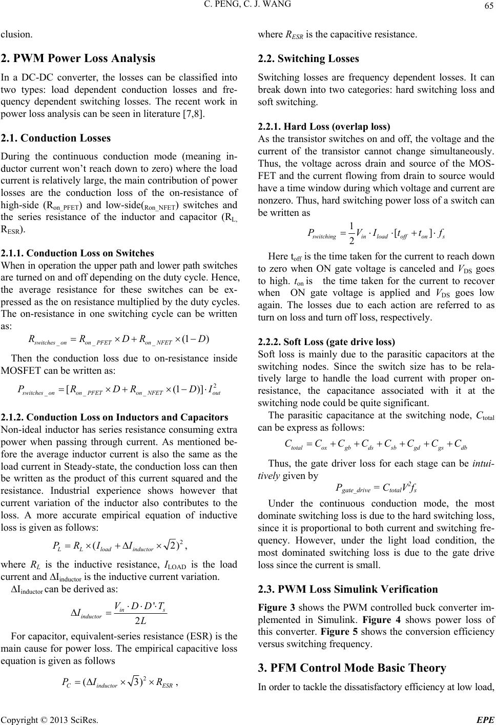 C. PENG, C. J. WANG 65 clusion. 2. PWM Power Loss Analysis be classified into 2.1. Conduction Losses duction mode (meaning in- 2.1.1. Conduction Loss on Switches ower path switches D Then the conduction loss due to on-resistance inside M (1)] where RESR is the capacitive resistance. uency dependent losses. It can verlap loss) off, the voltage and the In a DC-DC converter, the losses can two types: load dependent conduction losses and fre- quency dependent switching losses. The recent work in power loss analysis can be seen in literature [7,8]. During the continuous con ductor current won’t reach down to zero) where the load current is relatively large, the main contribution of power losses are the conduction loss of the on-resistance of high-side (Ron_PFET) and low-side(Ron_NFET) switches and the series resistance of the inductor and capacitor (RL, RESR). When in operation the upper path and l are turned on and off depending on the duty cycle. Hence, the average resistance for these switches can be ex- pressed as the on resistance multiplied by the duty cycles. The on-resistance in one switching cycle can be written as: __ _ (1 ) switches onon PFETon NFET RRDR OSFET can be written as: [2 __ _ s witches onon PFETon NFETout R D PRD I 2.1.2. Conduction Loss on Inductors and Capacitors a Non-ideal inductor has series resistance consuming extr power when passing through current. As mentioned be- fore the average inductor current is also the same as the load current in Steady-state, the conduction loss can then be written as the product of this current squared and the resistance. Industrial experience shows however that current variation of the inductor also contributes to the loss. A more accurate empirical equation of inductive loss is given as follows: 2 ( LL load PR I 2) inductor I , where RL is the inductive resistance, ILOAD s the load i current and ∆Iinductor is the inductive current variation. ∆Iinductor can be derived as: ' 2 in s inductor VDDT IL For capacitor, equivalent-series resistance (ESR) is the main cause for power loss. The empirical capacitive loss equation is given as follows 2 (3) C inductorESR PI R , 2.2. Switching Losses Switching losses are freq break down into two categories: hard switching loss and soft switching. 2.2.1. Hard Loss (o As the transistor switches on and current of the transistor cannot change simultaneously. Thus, the voltage across drain and source of the MOS- FET and the current flowing from drain to source would have a time window during which voltage and current are nonzero. Thus, hard switching power loss of a switch can be written as 1[] 2 s witchingin loadoffons VIttfP Here toff is the time taken for the current to reach down to asitic capacitors at the total zero when ON gate voltage is canceled and VDS goes to high. ton is the time taken for the current to recover when ON gate voltage is applied and VDS goes low again. The losses due to each action are referred to as turn on loss and turn off loss, respectively. 2.2.2. Soft Loss (gate drive loss) Soft loss is mainly due to the par switching nodes. Since the switch size has to be rela- tively large to handle the load current with proper on- resistance, the capacitance associated with it at the switching node could be quite significant. The parasitic capacitance at the switching node, C can be express as follows: totaloxgb d CCCC s sb gdgs db CCCC Thus, the gate driver loss for each stage can beui- tiv Under the conmode, the most do erification onverter im- Basic Theory t low load, int ely given by Pgate_drive = CtotalV2fs tinuous conduction minate switching loss is due to the hard switching loss, since it is proportional to both current and switching fre- quency. However, under the light load condition, the most dominated switching loss is due to the gate drive loss since the current is small. 2.3. PWM Loss Simulink V Figure 3 shows the PWM controlled buck c plemented in Simulink. Figure 4 shows power loss of this converter. Figure 5 shows the conversion efficiency versus switching frequency. 3. PFM Control Mode In order to tackle the dissatisfactory efficiency a Copyright © 2013 SciRes. EPE 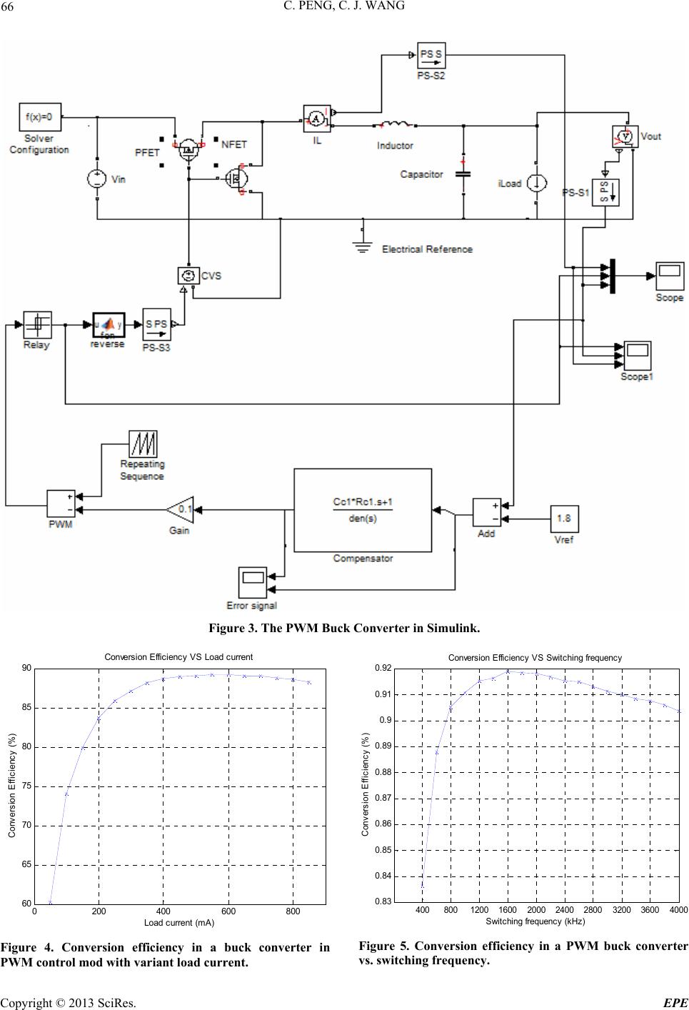 C. PENG, C. J. WANG Copyright © 2013 SciRes. EPE 66 Figure 3. The PWM Buck Converter in Simulink. 0200 400600 800 60 65 70 75 80 85 90 Conversion E ffici ency VS Load c urrent Load c urrent (m A) Conv ersion Ef f i c i ency (%) 4008001200 16002000 2400 28003200 36004000 0.83 0.84 0.85 0.86 0.87 0.88 0.89 0.9 0.92 0.91 Conversi on E ffic i ency VS S wi t chi ng frequenc y Swit chi ng frequency (kHz) Conversion Efficiency (%) Figure 5. Conversion efficiency in a PWM buck converter vs. switching frequency. Figure 4. Conversion efficiency in a buck converter i PWM control m o d with variant load current. n 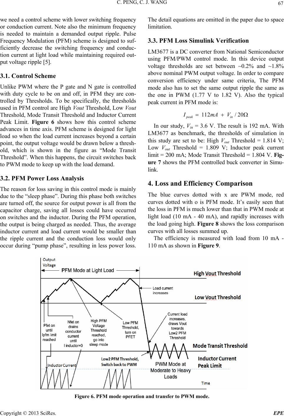 C. PENG, C. J. WANG 67 we need a control scheme with lower switching frequency or conduction current. Note also the minimum frequency is needed to maintain a demanded output ripple. Pulse Frequency Modulation (PFM) scheme is designed to suf- ficiently decrease the switching frequency and conduc- tion current at light load while maintaining required out- put voltage ripple [5]. 3.1. Control Scheme Unlike PWM where the P gate and N gate is controlled with duty cycle to be on and off, in PFM they are con- trolled by Thresholds. To be specifically, the thresholds used in PFM control are High Vout Threshold, Low Vout Threshold, Mode Transit Threshold and Inductor Current Peak Limit. Figure 6 shows how this control scheme advances in time axis. PFM scheme is designed for ligh would be drawn below a thresh- During this phase both switches for output power is all from the all losses could have occurred t load so when the load current increases beyond a certain point, the output voltage old, which is shown in the figure as “Mode Transit Threshold”. When this happens, the circuit switches back to PWM mode to keep up with the load demand. 3.2. PFM Power Loss Analysis The reason for loss saving in this control mode is mainly due to the “sleep phase”. are turned off, the source capacitor charge, saving on switches and the inductor. During the PFM operation, the output is being charged as needed. Thus, the average inductor current and load current would be smaller than the ripple current and the conduction loss would only occur during “pump phase”, resulting in less power loss. The detail equations are omitted in the paper due to space limitation. 3.3. PFM Loss Simulink Verification LM3677 is a DC converter from National Semiconductor using PFM/PWM control mode. In this device output voltage thresholds are set between ~0.2% and ~1.8% above nominal PWM output voltage. In order to compare conversion efficiency under same criteria, The PFM mode also has to set the same output ripple the same as the one in PWM (1.77 V to 1.82 V). Also the typical peak current in PFM mode is: 112 /20 peak in ImAV In our study, Vin = 3.6 V. The result is 192 mA. With LM3677 as benchmark, the thresholds of simulation in this study are set to be: High Vout Threshold = 1.814 V; Low Vout Threshold = 1.809 V; Inductor peak current limit = 200 mA; Mode Transit Threshold = 1.804 V. Fig- ure 7 shows the PFM controlled buck converter in Simu- link. 4. Loss and Efficiency Comparison The blue curves dotted with x are PWM mode, red curves dotted with o is PFM mode. It’s easily seen that the loss in PFM is much lower than that in PWM mode at light load (10 mA - 40 mA), and rapidly increases with the load going high. Figure 8 shows the loss comparison curves with all losses summed up. The efficiency is measured with load from 10 mA - 110 mA as shown in Figure 9. Figure 6. PFM mode operation and transfer to PWM mode. Copyright © 2013 SciRes. EPE 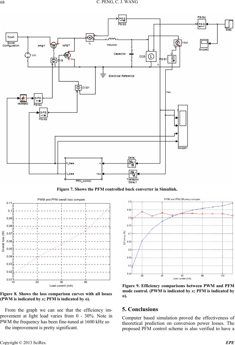 C. PENG, C. J. WANG 68 Figure 7. Shows the PFM c o ntrolled buck converter in Simulink. 10 2030 40 0.01 0.02 0.03 0.04 0.05 0.06 0.07 0.08 0.09 0. 1 0.11 P WM and PF M overall l os s c om pare Load c urrent (m A) Overall loss (W) Figure 8. Shows the loss comparison curves with all losses (PWM is indicated by x; PFM is indicated by o). Figure 9. Efficiency comparisons between PWM and PFM mode control. (PWM is indicate d by x; PFM is indicated by o). From the graph we can rovement at light load varies from 0 - 30%. Note in PWM the frequency has been fine-tuned at 1600 kHz so the improvement is pretty significant. Computer based simulation proved the effectiveness of theoretical prediction on conversion power losses. The proposed PFM control scheme is also verified to have a see that the efficiency im-5. Conclusions p Copyright © 2013 SciRes. EPE  C. PENG, C. J. WANG 69 significant improvement on conversion efficiency at light load (as high as 30%). REFERENCES [1] J. D. Chen, “Determine Buck Converter Efficiency in PFM Mode,”2007. www.powerelectronics.com [2] A. Harry, E. Robert and M. Dragan “DC-DC Converter Design for Battery-Operated Systems,” 26th Annual IEEE Power Electronics Specialists Conference, CO 80309-0425 USA, 1998. [3] S. Donald and C. Jorge, “Buck-Converter Design Demys- tified,”California, 2006. www.powerelectronics.com [4] “LM3677 3MHz, 600mA Miniature Step down DC-DC Converter for Ultra Low Voltage Circuits National Semiconductor,” Vol. 7, 2007. [5] K. B. Naima, C. Wen, A. Prashant and J. Elec Electron, “FPGA-Based Combined PWM-PFM Technique to Con- trol DC-DC Converters in Portable Devices,” Vol. 1, p. 102. doi:10.4172/2167-101X.1000102 [6] M. Rahimi, P. Parviz, and A. Peyman, “Application Note AN-1162 Compensator Design Procedure for Buck Con- verter with Voltage-Mode Error-Am-plifier,” www.irf.com [7] K. Saurabh, “Analysis, Design and Modeling of Dc-Dc Converter Using Simulink,” 2004. [8] P. Jeff, “An Efficient Frequency Controlled PFM for DC-DC Converters,” Electronic Theses and Dissertations Theses, Vol. 29, 2010. Copyright © 2013 SciRes. EPE |