Optics and Photonics Journal, 2013, 3, 252-255
doi:10.4236/opj.2013.32B059 Published Online June 2013 (http://www.scirp.org/journal/opj)
10 Gb/s Optical Interconnection on Flexible Optical
Waveguide in Electronic Printed Circuit Board
Shih-Hsiang Hsu1, Chih-Yuan Tsou1, Chih-Ming Wang1, Sheng-Chieh Tseng2
1Department of Electronic Engineering, National Taiwan University of Science and Technology, Chinese Taipei.
2Image Transfer Technology Department R & D Division, Compeq Manufacturing Co., LTD, Taoyuan, Chinese Taipei.
Email: shsu@mail.ntust.edu.tw
Received 2013
ABSTRACT
In this paper, we proposed 10 Gb/s transmission using 4-channel polymer waveguides on the optical electronic printed
circuit board. It was simulated by the ray tracing method for tolerance study of optical interconnection and fabrication.
In order for easy fabrication and high position accuracy, the polymer waveguides were forming silver coated 45° reflec-
tive mirrors by dicing method and e-beam deposition for 90° light beam turning. The coupling loss was demonstrated in
different polishing grit sizes. The optical interconnection in board-embed 4-channel flexible waveguides was demon-
strated with a low propagation loss of 0.1 dB/cm and a clear eye diagram at 2.5 Gb/s data rate per channel.
Keywords: Flexible Waveguide; Optical Electronic Printed Circuit Board
1. Introduction
The optical interconnection is a promising candidate to
resolve the issues from the technical problems of electri-
cal interconnections such as the upper limitation of trans-
mission data speed, electric power consumption, crosstalk,
and electromagnetic interference. [1,2]. The optical fi-
bers have large advantage in long distance interconnec-
tion due to their low propagation loss, light weight, low
cost, and immunity to electromagnetic interference. For
in-device optical interconnection, the optical polymer
waveguide transmission is better than fiber because of its
easy fab- rication, productivity and enabling high density
integra- tion in folded-type mobile device requirements.
Some research combines flexible optical polymer
waveguide and print circuit board (PCB) to realize flexi-
ble data transmission and optical electrical integration
[3,4]. In order to realize the board-to-board or chip-to-
chip inter- connection, the vertical coupling into optical
waveguide had been studied, which included the 90º-bent
fiber blocks [5], laser ablation processing [6], micro
prisms [7], and dicing processing [3,4].
In this paper, we have fabricated a flexible optical
waveguide (FOW) typed electronic printed circuit board
(EPCB), which is containing flexible optical waveguide
and electrical PCB. The waveguide terminal was made as
45º mirrors for vertical light beam coupling using dicing
processing. The optical loss due to unexpected fabrica-
tion process and waveguide terminal roughness issue was
also discussed.
2. Conceptual Structure
The optical interconnection conceptual structure for
FOW typed EPCB is composed by the flexible polyimide
substrate with optical waveguides, rigid PCB mounting
vertical-cavity surface-emitting laser (VCSEL) and pho-
todiode (PD) as shown in Figure 1.
The optical waveguide cross-section on the inputs is
illustrated in Figure 1(b). The refractive indices for the
waveguide cladding and core layers were 1.551 and
1.585, respectively. The polyimide waveguide core size
Figure 1. (a) FOW typed EPCB top view. (b) Wa vegu id e cross-
section on the inputs. (c) Optical path in cross-se c tion.
Copyright © 2013 SciRes. OPJ
S.-H. HSU ET AL. 253
is 50 μm × 50 μm, and the upper cladding thickness is 25
μm and lower one is 30 μm. The optical path in the FOW
is illustrated in Figure 1 (c). The VCSEL and PD area
are 20 μm and 90 μm respectively. The light emitting
from VCSEL to flexible polyimide waveguide was cou-
pled by the silver coated 45° mirror. Then, the light is
transmitted in the optical waveguide and vertically cou-
pled to PD by the opposite silver mirror.
3. Optical Interconnection Loss for FOW
The ray trace simulation demonstrated that the optical
interconnection loss from VECEL to PD was less than
0.1 dB. The investigation for the process tolerance and
multilayer structure misalignment is crucial in FOW
typed EPCB. In Figure 2, the optical loss in different
mirror angles and VCSEL/PD height away from the
waveguide surface (H) are considered. The simulation
results were showing that the VCSEL/PD height could
achieve lower optical loss and there was no obvious loss
difference, less than 0.5 dB, between the mirror angles
from 44º to 46º. The optical loss was less than 1 dB
while the VCSEL and PD were mounted at 75 μm away
from the waveguide surface. Besides, the lower H owns
the higher alignment tolerance for the mirror. Hence, the
angle and height precisely control during process are
important.
To simulate another optical alignment tolerance be-
tween mirror and VSCEL/PD, the horizontal directional
shift (X-axis and Z-axis) was considered as shown in
Figure 3. The loss due to 20 μm misalignment was about
2 - 3dB.
40 41 42 4344454647 48 49 50
0
1
2
3
4
5
6
L o ss (d B )
Angle
H=0 m
H=50 m
H=75 m
H=100 m
H=130 m
Figure 2. Mirror angle tolerance calculation.
4. Fabrication and Measurement of FOW
Typed EPCB
We fabricated a flexible multimode waveguide by using
the film shaped optical waveguide materials, enabling
easier film thickness control and handling. To make the
channel optical waveguide, the core layer was laminated
by a roll-to-roll method and the pattern was defined by
UV exposure through a photo mask and followed by the
development. After the thermal curing, an over-clad
sheet was covered, being thermally compressed with the
same condition with the under-clad lamination process,
as shown in Figure 4.
The fabricated flexible waveguide reliability was
evaluated as follows. A high-temperature/humidity test at
85 ºC /85%RH for 1000h were carried out. There was no
detectable peeling-off or separation occurred among any
layers. It indicates that the developed materials and fab-
ricated waveguide are demonstrating the high reliability.
Moreover, the bending measurements for optical loss and
-20-1001 02 0
0
1
2
3
4
5
6
H=0 m
H=25m
H=50m
H=75m
H=100 m
Loss (dB)
X Position Shift (m)
(a)
-20-1001 02 0
0
1
2
3
4
5
6 H=0m
H=25 m
H=50 m
H=75 m
H=100 m
L o ss ( dB)
Z Position Shift (m)
(
b
)
Figure 3. (a) X position and (b) Z position shift tolerance
calculation.
Figure 4. CCD image of waveguide cross-section.
Copyright © 2013 SciRes. OPJ
S.-H. HSU ET AL.
254
fatigue were carried out to evaluate the bending proper-
ties of flexible waveguides. The results of bending fa-
tigue test with conditions of bending angle from 0 to 180
degrees and 2-mm bending radius were showing the loss
was increased lower than 0.2 dB after ten thousand repe-
titions.
In order to evaluate the total loss of the FOW typed
EPCB, we analyzed the waveguide propagation loss,
reflective mirror loss and coupling loss from the mirror
to waveguide.
The propagation loss and coupling loss of the flexible
waveguide were analyzed by a cutback method. The
propagation loss was about 0.1 dB/cm measured with a
VCSEL light source at wavelength of 850 nm. The
waveguide coupling loss in different waveguide terminal
surface was shown in Figure 5. In this structure, two
kinds of waveguide terminal surfaces, 45° surface for
90° beam turning and vertical surface for light into/out of
the waveguide were demonstrated. The samples were
polished with different polishing films which had the grit
sizes of 0.1-μm, 1-μm, 3-μm, and 9-μm. The dia-
mond-blade method was utilizing the grit size of 1 - 2
μm and the 4 and 9 surfaces with spindle
speed 24000 rpm were fabricated and cut speed 0.5 mm/s,
as shown in Figure 6. The 45°surface angle error was
within 45 ± 1°. The waveguide end surface image and
coupling loss were also shown in Figures 7 and 8, re-
spectively.
Figure 5. Photo image for FOW typed EPCB.
Figure 6. Diamond-blade method.
Figure 7. Waveguide termin a l surface image .
02468
0
1
2
3
4
5
10
P o lis hin g me th o d
Diam ond-blade method
Waveguide Coupling Loss (dB)
Grit Size (m)
Figure 8. Waveguide coupling loss between different
waveguide terminal surfaces.
The Ag reflection from 4mirrors was deposited by
the e-beam evaporation process and the thickness was
about 400 nm on the waveguide terminal 45°-ended.
The vertical incident light source into the 45°-mirror
causes the optical loss less than 0.8 dB from 90°turning
points.
Moreover, the bending loss and bending fatigue were
carried to evaluate the flexible waveguide reliability. The
bending fatigue characterization was showing that the
excess loss was lower than 0.2 dB after one hundred
thousand of 0°- 180°bends with 2-mm bending radius.
To measure the transmission quality from VCSEL to
PD of the interconnection module, a DC voltage of 3.3 V
was supplied into the transmitter and the current gener-
ated in receiver was characterized. In Figure 9, it shows
that the implementation and integration were imple-
mented for the proposed active electro-optical bus mod-
ule. A 1×4 VCSEL array and a 1×4 PD array both with
2.5 Gbps/channel are directly die-bonded on the trans-
mission and the receiving boards, working with 2.5 Gbps
driver chips, amplifiers, and other active/passive devices.
An electric signal of clear 2.5 Gb/s generated by a pulse
pattern generator was supplied to the transmitter module
through the SMA connector and the signals transmitted
Copyright © 2013 SciRes. OPJ
S.-H. HSU ET AL.
Copyright © 2013 SciRes. OPJ
255
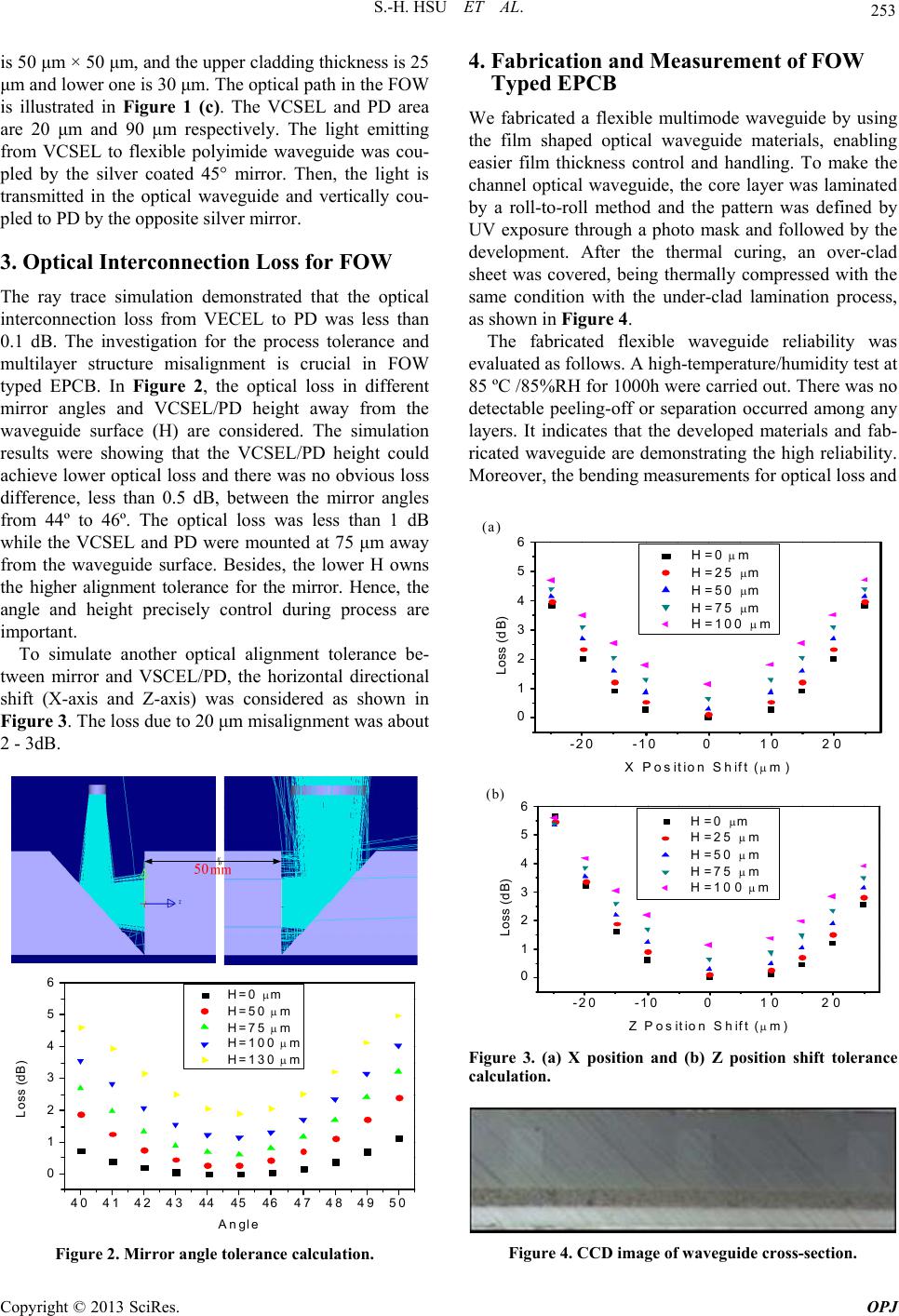
to the receiver module through the waveguide with SONET
OC-48 eye mask as shown in Figure 10. As a result, the
eye diagram of the electrical output signal from the receiver
on flexible opto-electrical interconnect module was
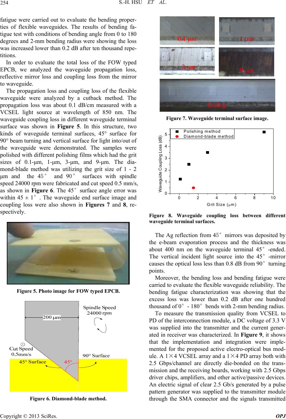
tested with network analyzer and shown in Figure 11.
5. Conclusions
In this paper, the optical interconnection loss in FOW
typed EPCB was discussed for fabrication tolerance
study. The optical loss variation due to mirror angles
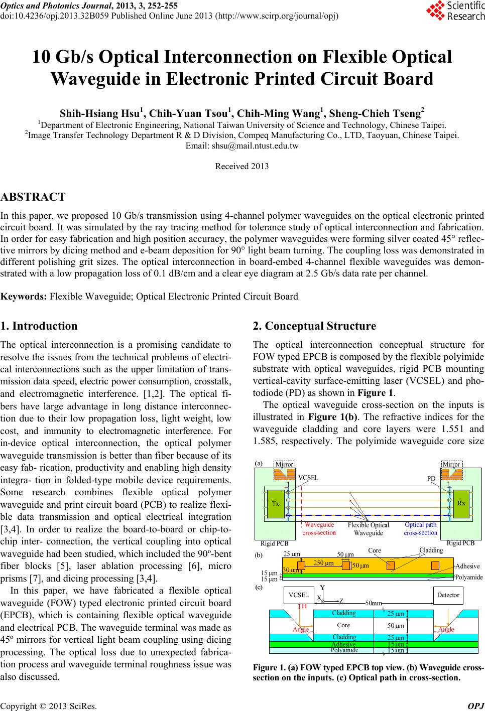
Figure 9. (a) Transmitter and (b) receiver active electro-
optical module with 4-channel VECSEL array and PD ar-
ray respectively.
Figure 10. 2.5 Gb/s Eye diagram for one channel polymer
waveguide.
Figure 11. 2.5 Gb/s eye-diagram per channel for the FOW
typed EPCB at 180° bend.
from 44° to 4 was less than 0.5 dB. The dia-
mond-blade method was applied and implemented on the
45±1° mirror. The waveguide coupling loss was dis-
cussed by different waveguide terminal surfaces. The
diamond-blade method could provide smooth surface
and low coupling loss. A prototyped FOW combined
with EPCB was fabricated and demonstrating the propa-
gation loss and mirror coupling loss as 0.1 dB/cm and
0.8 dB, respectively. After one hundred thousand of 0°-
180°bending fatigue tests, the propagation loss was
increased lower than 0.2 dB. An EPCB typed the optical
flexible waveguide and electrical rigid PCB was verified
and its performance achieved practical applications for
the optical interconnection. We also confirmed that a
4-ch VCSEL array and a 4-ch PD array could success-
fully transmit light signals at a speed of 2.5 Gb/s per
channel.
6. Acknowledgements
This paper was financially supported by the National
Science Council of the Republic of China, Taiwan, under
the contract NSC 101-3113-P-011-003 and the collabora-
tion project with the Compeq Manufacturing Co., LTD.
REFERENCES
[1] S. Uhlig and M. Robertsson, “Limitations to and Solu-
tions for Optical Loss in Optical Backplanes,” Journal of
Lightwave Technology, Vol. 24, 2006pp. 1710-1724.
doi:10.1109/JLT.2006.870978
[2] D. A. B. Miller, “Rationale and Challenges for Optical
Interconnects to Electronic Chips,” Proceedings of the
IEEE, Vol. 88, 2000, pp. 728-749.
doi:10.1109/5.867687
[3] B. S. Rho, W. J. Lee, J. W. Lim, G. W. Kim, C. H. Cho,
and S. H. Hwang, “High-Reliability Flexible Optical
Printed Circuit Board for Opto-Electric Interconnec-
tions,” Opti cal Engin eering, Vol. 48, 2009.
[4] T. Shibata and A. Takahashi, “Flexible Opto-Electronic
Circuit Board for In-Device Interconnection,” Lake
Buena Vista, FL, 2008, pp. 261-267.
[5] S. H. Hwang, M. H. Cho, S. K. Kang, H. H. Park, H. S.
Cho, S. H. Kim, K. U. Shin and S. W. Ha, “Passively
Assembled Optical Interconnection System Based on An
Optical Printed-Circuit Board,” IEEE Photonics Tech-
nology Letters, Vol. 18, 2006 pp. 652-654.
doi:10.1109/LPT.2006.87012 7
[6] E. Bosman, J. Missinne, B. V. Hoe, G. V. Steenberge, S.
Kalathimekkad, J. V. Erps, I. Milenkov, K. Panajotov, T.
V. Gijseghem, P. Dubruel, H. Thienpont and P. V. Daele,
“Ultrathin Optoelectronic Device Packaging in Flexible
Carriers,” IEEE Journal on Selected Topics in Quantum
Electronics, Vol. 17, 2011, pp. 617-628.
doi:10.1109/JSTQE.2010.20 96407
[7] M. Karppinen, T. Alajoki, A. Tanskanen, K. Kataja, J. T.
Mäkinen, P. Karioja, M. Immonen and J. Kivilahti, “Par-
allel Optical Interconnect between Surface-Mounted De-
vices on FR4 Printed Wiring Board Using Embedded
Waveguides and Passive Optical Alignments,” Stras-
bourg, 2006.