Paper Menu >>
Journal Menu >>
 Optics and Photonics Journal, 2013, 3, 73-75 doi:10.4236/opj.2013.32B018 Published Online June 2013 (http://www.scirp.org/journal/opj) Design of High-speed Sampling System in Pulse Laser Application Jian Liu1, Ming-ai Lv2, Jiang Wang2 1The Engineering & Technical College, Chengdu University of Technology, Leshan, China 2Southwest Institute of Technical Physics, Chengdu, China Email: emailofliujian@126.com Received 2013 ABSTRACT In measurement system by means of pulse laser, such as plasma measuring, laser ranging, the amplitude of echoed laser wave is very weak and difficult to detect by traditional analog electronic technology. A digital high speed data acquisi- tion and processing system was designed to meet the accuracy requirement. It adopted high speed AD chip and advan- tage FPGA chip as core unit. Experiment results have verified this system can reach to 1GHz sample rate and can catch weak echo wave effectively and the measuring accuracy is improved markedly. Keywords: Pulse Laser; Echo Wave Detecting; High Speed AD; FPGA 1. Introduction In many engineering application, such as plasma charac- teristics measuring, laser ranging, remote dust concentra- tion measuring, and so on, the pulse laser technology were adopted widely[1-4]. As the precision requirement is higher, the pulse width is narrower, and the echo wave energy received by the detector is lower. Under this cir- cumstance, even the received signal has been amplified highly, it is very weakly still. In recently application system of pulse laser, the pulse could be compressed to narrower than 5 ns. But because of the spread effect of plasma or atmosphere, the pulse would be broadened about to 5 - 15 ns. When the breadth became narrower and plasma density became higher, the amplitude of the echo pulse signal received by measuring system became weaker rapidly, and traditional analog electronic system couldn't catch it. Figure 1 shows a common receiving wave picture on oscilloscope of these cases. Figure 1. Typical received echo wave pulse. To deal with such cases, a pulse signal detecting and processing system was designed. It adopted high speed AD device and the fast data processing ability of FPGA. This system can well work under condition of low signal to noise ratio (SNR), narrow pulse width, little echo wave amplitude. In the system, the AD chip ADC08D1000 which work in 1 GHz sampling rate, and the EP2S60 FPGA chip, are applied as core components. 2. System Design 2.1. High Speed Sampling Sub-system To realize digital sampling of pulse signal, a AD subsys- tem was designed firstly, and the sketch of its structure is shown in Figure 2. Sampling rate of the AD chip was controlled by external clock, and the output of sample data was in differential format to enhance capacity of resistant disturbance. In the same time, an accompany clock was outputted to lock the phase of the multiplexed output of sample data. In order to improve the measuring accuracy, the width of pulse laser would be narrow as possible. In this system, the pulse is 5 ns width. It required the AD device was in very high sampling rate, and then ADC08D1000 was selected because it had two-channel sample function and Diff data output Diff clk output Control signals Diff clk input AD Laser pulse input Figure 2. Sketch of high speed sampling subsystem. Copyright © 2013 SciRes. OPJ 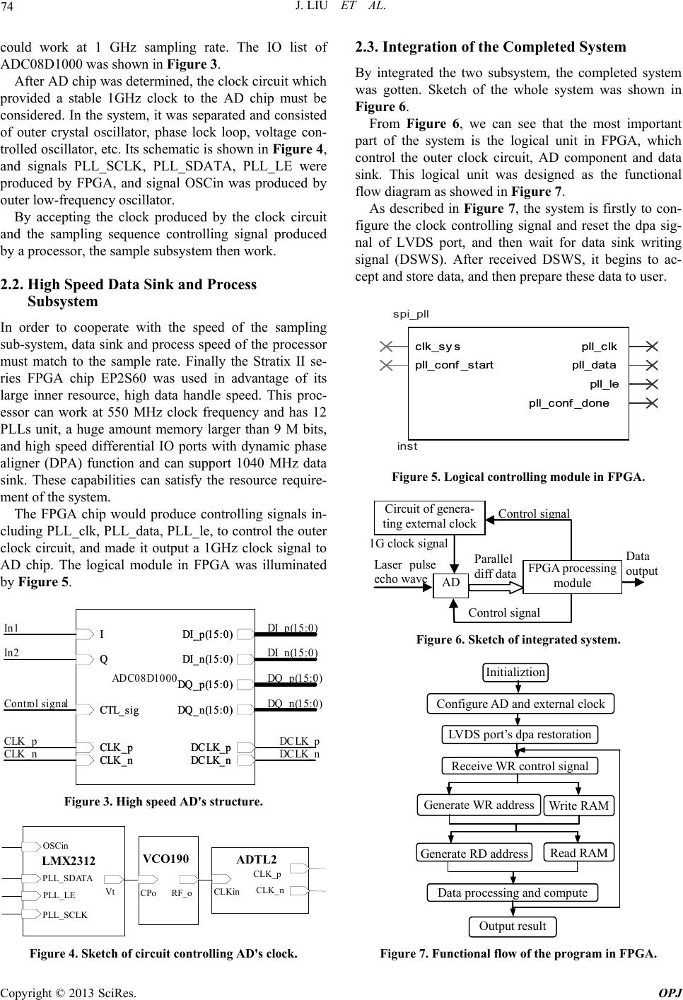 J. LIU ET AL. 74 could work at 1 GHz sampling rate. The IO list of ADC08D1000 was shown in Figure 3. After AD chip was determined, the clock circuit which provided a stable 1GHz clock to the AD chip must be considered. In the system, it was separated and consisted of outer crystal oscillator, phase lock loop, voltage con- trolled oscillator, etc. Its schematic is shown in Figure 4, and signals PLL_SCLK, PLL_SDATA, PLL_LE were produced by FPGA, and signal OSCin was produced by outer low-frequency oscillator. By accepting the clock produced by the clock circuit and the sampling sequence controlling signal produced by a processor, the sample subsystem then work. 2.2. High Speed Data Sink and Process Subsystem In order to cooperate with the speed of the sampling sub-system, data sink and process speed of the processor must match to the sample rate. Finally the Stratix II se- ries FPGA chip EP2S60 was used in advantage of its large inner resource, high data handle speed. This proc- essor can work at 550 MHz clock frequency and has 12 PLLs unit, a huge amount memory larger than 9 M bits, and high speed differential IO ports with dynamic phase aligner (DPA) function and can support 1040 MHz data sink. These capabilities can satisfy the resource require- ment of the system. The FPGA chip would produce controlling signals in- cluding PLL_clk, PLL_data, PLL_le, to control the outer clock circuit, and made it output a 1GHz clock signal to AD chip. The logical module in FPGA was illuminated by Figure 5. Q I CTL_sig CLK_p DI_p(15:0) DI_n(15:0) DQ_p(15:0) DQ_n(15:0) DC LK_p CLK_n DC LK_n ADC08D1000 Q I CTL_sig CLK_p DI_p(15:0) DI_n(15:0) DQ_p(15:0) DQ_n(15:0) DC LK_p CLK_n DC LK_n In1 In2 Control signal CLK_p CLK_n DCLK_n DC LK_p DQ_n(15:0) DQ_p(15:0) DI_n(15:0) DI_p(15:0) Figure 3. High speed AD's structure. CPo PLL_SDATA PLL_SCLK PLL_LE LMX2312 OSCin Vt RF_o VCO190 CLKin CLK_p CLK_n ADTL2 Figure 4. Sketch of circuit controlling AD's clock. 2.3. Integration of the Completed System By integrated the two subsystem, the completed system was gotten. Sketch of the whole system was shown in Figure 6. From Figure 6, we can see that the most important part of the system is the logical unit in FPGA, which control the outer clock circuit, AD component and data sink. This logical unit was designed as the functional flow diagram as showed in Figure 7. As described in Figure 7, the system is firstly to con- figure the clock controlling signal and reset the dpa sig- nal of LVDS port, and then wait for data sink writing signal (DSWS). After received DSWS, it begins to ac- cept and store data, and then prepare these data to user. spi_pll inst clk_sysclk_sys pll_conf _startpll_conf _start pll_clkpll_clk pll_datapll_data pll_lepll_le pll_c onf_donepll_c onf_done Figure 5. Logical controlling module in FPGA. Circuit of genera- ting external clock AD FPGA processing module Laser pulse echo wave 1G clock signal Control signal Control signal Parallel diff data Data out p ut Figure 6. Sketch of integrated system. Initializtion Confi g ure AD and external clock LVDS port’s dpa restoration Generate WR address Receive WR control si g nal Write RAM Read RAM Data processing and compute Output result Ge n e rat e RD a dd r ess Figure 7. Functional flow of the program in FPGA. Copyright © 2013 SciRes. OPJ 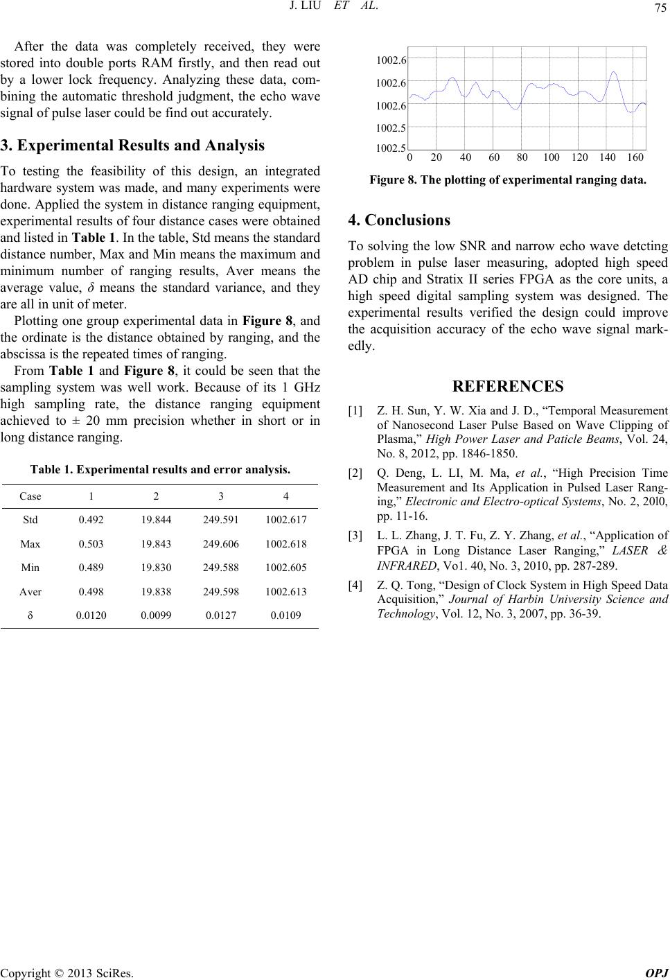 J. LIU ET AL. Copyright © 2013 SciRes. OPJ 75 Aere st tegrated perimental data in Figure 8, and th n that the sa Table 1. Experimental results and error analysis. Case 1 2 3 4 fter the data was completely received, they w 020406080 100 120 140160 1002.5 1002.5 1002.6 1002.6 1002.6 ored into double ports RAM firstly, and then read out by a lower lock frequency. Analyzing these data, com- bining the automatic threshold judgment, the echo wave signal of pulse laser could be find out accurately. 3. Experimental Results and Analysis To testing the feasibility of this design, an inFigure 8. The plotting of experimental ranging data. hardware system was made, and many experiments were done. Applied the system in distance ranging equipment, experimental results of four distance cases were obtained and listed in Ta b le 1 . In the table, Std means the standard distance number, Max and Min means the maximum and minimum number of ranging results, Aver means the average value, δ means the standard variance, and they are all in unit of meter. Plotting one group ex 4. Conclusions To solving the low SNR and narrow echo wave detcting problem in pulse laser measuring, adopted high speed AD chip and Stratix II series FPGA as the core units, a high speed digital sampling system was designed. The experimental results verified the design could improve the acquisition accuracy of the echo wave signal mark- edly. e ordinate is the distance obtained by ranging, and the abscissa is the repeated times of ranging. From Table 1 and Figure 8, it could be seeREFERENCES mpling system was well work. Because of its 1 GHz high sampling rate, the distance ranging equipment achieved to ± 20 mm precision whether in short or in long distance ranging. [1] Z. H. Sun, Y. W. Xia and J. D., “Temporal Measurement of Nanosecond Laser Pulse Based on Wave Clipping of Plasma,” High Power Laser and Paticle Beams, Vol. 24, No. 8, 2012, pp. 1846-1850. [2] Q. Deng, L. LI, M. Ma, et al., “High Precision Time Measurement and Its Application in Pulsed Laser Rang- ing,” Electronic and Electro-optical Systems, No. 2, 20l0, pp. 11-16. Std 0.492 19.249.1 1002.17 844 596 [3] L. L. Zhang, J. T. Fu, Z. Y. Zhang, et al., “Application of FPGA in Long Distance Laser Ranging,” LASER & INFRARED, Vo1. 40, No. 3, 2010, pp. 287-289. M 0. ax 0.503 19.843 249.606 1002.618 Min 0.489 19.830 249.588 1002.605 Aver 0.498 19.838 249.598 1002.613 δ 0120 0.0099 0.0127 0.0109 [4] Z. Q. Tong, “Design of Clock System in High Speed Data Acquisition,” Journal of Harbin University Science and Technology, Vol. 12, No. 3, 2007, pp. 36-39. |