Paper Menu >>
Journal Menu >>
 Journal of Modern Physics, 2010, 1, 360-363 doi:10.4236/jmp.2010.16051 Published Online December 2010 (http://www.SciRP.org/journal/jmp) Copyright © 2010 SciRes. JMP A Dependence of Crystallinity of In2O3 Thin Films by a Two-Step Heat Treatment of Indium Films on the Heating Atmosphere Yuichi Sato, Fumito Otake, Hirotoshi Hatori Graduate School of Engineering and Resource Science, Akita University, 1-1, Tegata, Akita, Japan E-mail: yusato@ipc.akita-u.ac.jp Received July 25, 201 0; revised August 28, 2010; September 3, 2010 Abstract A difference in crystallinity of In2O3 thin films on sapphire substrates by heat treatment of indium films was reported. Indium films were heated in an inert atmosphere or in air until they reached a specified temperature and then oxidized in air at much higher temperatures. Crystallinity of the In2O3 thin film which was heat-treated in air from room temperature was quite poor. On the other hand, narrow X-ray rocking curves of the In2O3 films were obtained when the temperature was increased in an inert atmosphere to a specified tem- perature. Keywords: Solid Phase Epitaxy, Oxides, Sapphire, Semiconducting Materials 1. Introduction Recently, single-crystal sapphire wafers have been used widely as substrates for heteroepitaxial growth of semi- conductor thin films such as gallium nitride (GaN) [1]. Sapphire is a transparent material, therefore, practical applications of it to such as transparent substrates for single-crystalline thin film photovoltaic cells have been also expected. However, it is relatively difficu lt to collect electric currents effectively in the thickness direction of the semiconductor thin films because sapphire is also an insulating material. Therefore, to allow electric currents to flow effectively to the thickness direction of the semiconductor thin film some conductive layers should be formed between the sapphire substrate and the semi- conductor thin film. Indium oxide (In2O3), which is a wide band gap mate- rial, is widely used as a transparent conducting film. It is usually prepared by sputtering techniques [2] and het- eroepitaxy of In2O3 on sapphire substrates have been also investigated by using various techniques such as atomic layer deposition [3], pulsed laser deposition [4] and reac- tive magnetron sputtering [5] methods. As In2O3 has a cubic crystal structure [6], it can has a heteroepitaxial relationship between [111] In2O3 and [0001] sapphire. In such case, In2O3 film will grow epitaxially on the sap- phire substrate. In addition, another semiconductor thin film which will be formed on the In2O3 film will also grow epitaxially on it if the semiconductor has a het- eroepitaxial relationship to In2O3. Therefore, the semi- conductor thin film will have better properties than films grown on polycrystalline or amorphous underlayers. As an example for it, we have epitaxially grown In2O3 thin films on sapphire substrates by a sputtering method and grown Cadmium Telluride (CdTe) thin films on the un- derlayers [7]. In the experiment, the CdTe thin films could be epitaxially grown on the In2O3 thin films with- out deterioration compared with CdTe thin films grown directly on sapphire substrates. Metal indium thin films can be quite easily deposited using simple and inexpensive vacuum evaporation tech- niques. In addition, indium can be readily oxidized by heating at a low temperature in an atmosphere containing oxygen. Therefore, it may be possible to easily produce indium oxide thin films using simple evaporation and oxidization processes. Furthermore, performing this processing by laser radiation heating will permit local oxidization of indium thin films, enabling the transpar- ency and conductivity of the films to be locally con- trolled. From the easiness and possibility for expansion of the process utility, we have considered that it is worth to develop this processing method. The ultimate goal of our research is to obtain het- eroepitaxially grown In2O3 thin films on single-crystal  Y. SATO ET AL.361 sapphire substrates by using the above-mentioned simple techniques. In the pursuit of this goal, we observed dif- ferent crystallinities of In2O3 thin films that had been heat treated by a two-step heat treatment. This difference depended on the atmosphere used in the two-step heat treatment. In this paper, we report the effect of the heat- treatment atmosphere on the crystallinity of In2O3 thin films obtained by the two-step heat treatment of metal indium thin films. 2. Experiments Indium thin films were deposited by using a vacuum evaporation system with a resistive heater for evaporat- ing indium shots (6 N). Sapphire (0001) single-crystal wafers and synthetic quartz glass plates for comparison were used as substrates. The indium thin films were about 100 nm thick. After deposition, the indium thin films were heat treated in an infrared heating furnace and oxidized to form In2O3 thin films. The heat treatment patterns are schematically shown in Figure 1. In the first step of the heat treatment, the temperature was increased from room temperature to 500℃ in an inert N2 atmos- phere or air. In the second step, the inert atmosphere was replaced with air when the temperature reached to 500℃, then the temperature was increased to 900℃ and maintained for 1 h. Crystallinities of the obtained thin films were evaluated by X-ray diffraction (XRD). 3. Results and Discussion First, indium thin films that had been deposited on quartz glass substrates were conventionally heat treated in air for 1 h at various temperatures. Figure 2 shows the XRD patterns of the obtained thin films. In this case, the tem- perature was increased from room temperature in air (i.e., not in an inert atmosphere). The indium thin films gradu- ally become oxidized with increasing heat-treatment tem- perature. The diffraction peaks for metal indium are not visible when the heat-treatment temperature exceeds 500℃. Thus, In2O3 thin films are obtained when the heat-treatment temperature exceeds 500℃. In addition, it is considered that crystallization of the In2O3 thin films progresses with increasing heat-treatment temperature as the X-ray intensity of In2O3 increases by increasing the temperature. Figure 3 shows X-ray rocking curves (XRCs) of the In2O3 (222) peaks of films prepared on sapph ire and quart z glass substrates. The films were produced by a conven- tional single-step heat treatment in air at 900℃ for 1 h with no inert atmosphere. The XRC of the In2O3 thin film obtained on sapphire substrate is broad and almost (a) (b) Figure 1. Heat treatment schematics of (a) the two-step heat treatment using inert atmosphere tried in this work and (b) conventional single-step heat treatment with no inert at- mosphere. In the two-step treatment, the temperature was increased in an inert atmosphere to 500℃ and then the inert atmosphere was replaced with air. same with that obtained on quartz glass substrate, that is, crystallinity of the film is quite poor. There is no differ- ence in the XRCs of the films prepared on the sin- gle-crystal sapphire and quartz glass substrates despite In2O3 having a heteroepitaxial relationship with the sap- phire substrate. This implies that there is no epitaxial effect from the single-crystal sapphire substrate to the In2O3 thin film. This is considered to be because the melting point of indium is about 157℃, so that indium thin films may be oxidized at this low temperature, which causes their recrystallization temperature to in- crease abruptly. Therefore, films that have been oxidized at low temperatures are not able to recrystallize when heat treated in an atmosphere containing oxygen. Con- sequently, In2O3 films prepared on a single-crystal sap- Copyright © 2010 SciRes. JMP 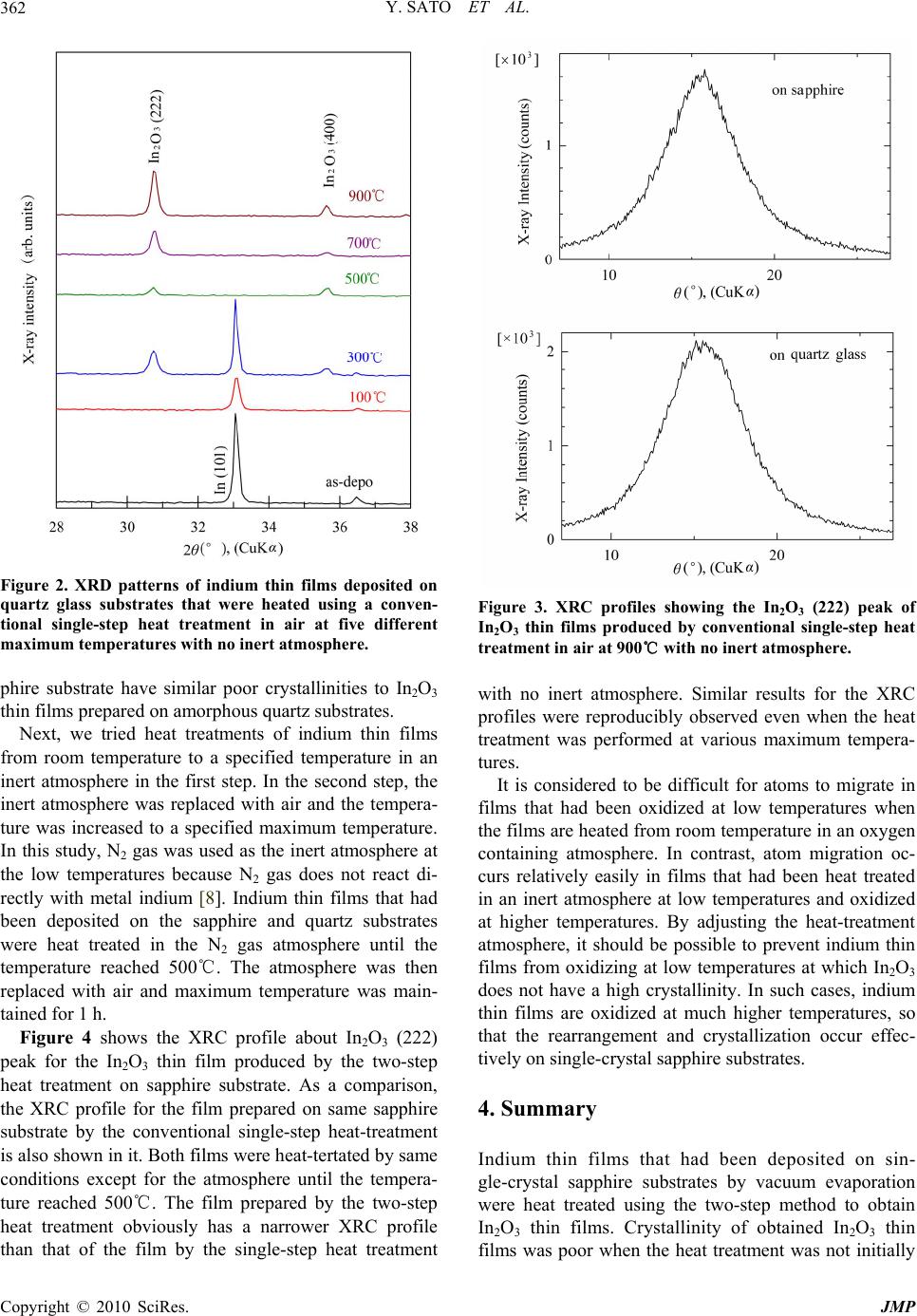 Y. SATO ET AL. 362 Figure 2. XRD patterns of indium thin films deposited on quartz glass substrates that were heated using a conven- tional single-step heat treatment in air at five different maximum temperatures with no inert atmosphere. phire substrate have similar poor crystallinities to In2O3 thin films prepared on amorphous quartz substrates. Next, we tried heat treatments of indium thin films from room temperature to a specified temperature in an inert atmosphere in the first step. In the second step, the inert atmosphere was replaced with air and the tempera- ture was increased to a specified maximum temperature. In this study, N2 gas was used as the inert atmosphere at the low temperatures because N2 gas does not react di- rectly with metal indium [8]. Indium thin films that had been deposited on the sapphire and quartz substrates were heat treated in the N2 gas atmosphere until the temperature reached 500℃. The atmosphere was then replaced with air and maximum temperature was main- tained for 1 h. Figure 4 shows the XRC profile about In2O3 (222) peak for the In2O3 thin film produced by the two-step heat treatment on sapphire substrate. As a comparison, the XRC profile for the film prepared on same sapphire substrate by the conventional single-step heat-treatment is also shown in it. Both films were heat-tertated by same conditions except for the atmosphere until the tempera- ture reached 500℃. The film prepared by the two-step heat treatment obviously has a narrower XRC profile than that of the film by the single-step heat treatment Figure 3. XRC profiles showing the In2O3 (222) peak of In2O3 thin films produced by conventional single-step heat treatment in air at 900℃ with no inert atmosphere. with no inert atmosphere. Similar results for the XRC profiles were reproducibly observed even when the heat treatment was performed at various maximum tempera- tures. It is considered to be difficult for atoms to migrate in films that had been oxidized at low temperatures when the films are heated from room temperature in an oxygen containing atmosphere. In contrast, atom migration oc- curs relatively easily in films that had been heat treated in an inert atmosphere at low temperatures and oxidized at higher temperatures. By adjusting the heat-treatment atmosphere, it should be possible to prevent indium thin films from oxidizing at low temperatures at which In2O3 does not have a high crystallinity. In such cases, indium thin films are oxidized at much higher temperatures, so that the rearrangement and crystallization occur effec- tively on single-crystal sapphir e substrates. 4. Summary Indium thin films that had been deposited on sin- gle-crystal sapphire substrates by vacuum evaporation were heat treated using the two-step method to obtain In2O3 thin films. Crystallinity of obtained In2O3 thin films was poor when the heat treatment was not initially Copyright © 2010 SciRes. JMP  Y. SATO ET AL. Copyright © 2010 SciRes. JMP 363 (a) (b) Figure 4. XRC profiles about the In2O3 (222) peak of In2O3 thin films obtained on sapphire substrates by (a) the two-step heat treatment and (b) conventional single-step treatment. In the two-step treatment, the temperature was increased in an inert atmosphere to 500℃ and then the inert atmosphere was replaced with air. performed in an inert atmosphere. In contrast, a clear difference and improvement in the crystallinity was ob- served when the temperature was increased from room temperature to a specified temperature in an inert at- mosphere in the first step prior to the second step of the heat treatment in an oxygen-containing atmosphere. Therefore, this kind of two-step heat treatment will be- come an effective method for producing epitaxially grown In2O3 thin films easily in the simple oxidation method of metal indium thin films. 5. References [1] S. Nakamura, “III-V Nitride-Based Light-Emitting Di- odes,” Diamond and Related Materials, Vol. 5, No. 3-5, 1996, pp. 496-500. [2] D. B. Fraser, “Sputter-Deposited Films for Display De- vices,” Thin Solid Films, Vol. 13, No. 2, 1972, pp. 407-412. [3] C. Wei-Hsu, Y. Kuo-Yi, L. Shao-Cian, G. Jyh-Rong, N. Cuo-Yo and L. Shih-Chang, “On the Physical Properties of In2O3 Films Prepared by Atomic Layer Deposition Using Tri-methyl-Indium and Nitrous Oxide,” Proceed- ings INEC 2010-2010 3rd International Nanoelectronics Conference, Hong Kong, January 2010, pp. 791-792. [4] R. K. Gupta, D. Brown, K. Ghosh, S. R. Mishra and P. K. Kahol, “Magneto-Transport Properties of Gd-doped In2O3 Thin Films,” Materials Research Society Symposium Pro- ceedings, Vol. 1032, 2008, pp. 77-81. [5] C. Lung-Chien, L. Wen-How, L. Ray-Ming, S. Hue-Tang and C. Hung-Chang, “Optical Properties of In2O3 Oxi- dized from InN Deposited by Reactive Magnetron Sput- tering,” Applied Surface Science, Vol. 252, No. 24, Oc- tober 2006, pp. 8438-8441. [6] JCPDS ed., “Powder Diffraction File,” International Centre for Diffraction Data, 1993. [7] H. Hatori, M. Arai, S. Igarashi, K. Ito, S. Kikuchi and Y. Sato, “Preparations of CdTe Thin Films on Sapphire Sub- strates Having Several Conducting Layers,” Proceedings of the 2010 IEICE General Conference, Sendai, March 2010, p. 18. [8] J. B. MacChesney, P. M. Bridenbaugh and P. B. O’Connor, “Thermal Stability of Indium Nitride at Ele- vated Temperatures and Nitrogen Pressures,” Materials Research Bulletin, Vol. 5, No. 9, 1970, pp. 783-792. |