Journal of Electromagnetic Analysis and Applications, 2013, 5, 288-293
http://dx.doi.org/10.4236/jemaa.2013.57045 Published Online July 2013 (http://www.scirp.org/journal/jemaa)
Resistor Loaded EBG Surfaces for Slot Antenna Design*
Shenyi Cao, Yunqi Fu
College of Electronic Science and Engineering, National University of Defense Technology, Changsha, China.
Email: shenyicao@gmail.com, yunqifu@nudt.edu.cn
Received May 21st, 2013; revised June 22nd, 2013; accepted July 2nd, 2013
Copyright © 2013 Shenyi Cao, Yunqi Fu. This is an open access article distributed under the Creative Commons Attribution License,
which permits unrestricted use, distribution, and reproduction in any medium, provided the original work is properly cited.
ABSTRACT
We present a resistor loaded EBG surface (REBG) for antenna design. Specifically, lumped resistors are embedded be-
tween periodic metal patches of mushroom like EBG structures. Surface wave propagation along the REBG surface is
analyzed as a periodically loaded transmission line model and low transmission bandgap is identified and experimen-
tally verified. The reflection properties of REBG surface to the incident electromagnetic waves are also studied. Slot
antenna is placed within the REBG surface. The REBG surface is used to suppress surface waves across the antenna
aperture, resulting in radiation performance improvement. Concurrently, the REBG surface can also absorb electro-
magnetic energy to reduce antenna radar cross section (RCS).
Keywords: EBG; Antenna; RCS
1. Introduction
Electromagnetic bandgap (EBG) structures have been
extensively explored in recent years. The most popular of
them is the mushroom like EBG structure printed on a
microstrip substrate composed of metal islands and ver-
tical connections to the ground plane [1]. This type of
EBG structure exhibits bandgap to suppress surface wave
propagation and in-phase reflection coefficient. It has
been shown [2,3] that suppression of surface waves leads
to improved radiation efficiency and antenna gain. Fur-
ther, side lobes can be reduced by eliminating surface
wave scattering from edges. Mutual coupling in phased
arrays can also be reduced using EBG structures [4] and
scan blindness can be suppressed [5,6].
EBG structures have also been used for antenna radar
cross section (RCS) control. For example, a metallic
EBG based radome was proposed in [7] to reduce an-
tenna RCS, but worked only when the antenna was
switched off. Their in-phase reflection properties have
also been exploited to realize ultra-thin radar absorbing
materials (RAM). Specifically, the EBG surface can be
covered by a lossy dielectric layer [8] or loaded with
lumped resistors placed between the adjacent metal
patches [9]. In [10] a similar RAM structure has been
used for antenna RCS reduction by welding resistors
interconnecting the metal patches. However, this design
did not suppress surface waves at the RCS reduction
frequency because it did not include vias to the substrate.
In this paper, we present a slot antenna design based
on resistor loaded EBG (REBG) surfaces. Waveguide slot
arrays in presence of REBG surfaces have already been
presented in [11]. This REBG surface did exhibit simul-
taneously surface wave suppression and absorption of the
incident wave over a specific frequency band. Therefore,
side lobes could be reduced by suppressing surface wave
radiation. The RCS was concurrently reduced.
We also considered the analysis of REBG surfaces.
Specifically, the surface wave propagation characteristics
of REBG are analyzed using the periodically loaded
transmission line model. An optimization of the REBG
based slot antenna is considered in terms of its return loss,
side lobes and antenna RCS. Finally, a comparison of
antennas on EBG and REBG ground planes is presented.
2. Resistor Loaded Mushroom EBG
Structure
2.1. Structure and Equivalent Circuit Model
The geometry of the REBG structure is displayed in Fig-
ure 1. Square patches of width w are periodically printed
on a grounded substrate (having thickness h and relative
permittivity r
). These patches are separated by a gap g
and lumped resistors of resistance R are welded between
adjacent patches. The circuit model of the REBG surface
could then be represented by a parallel RLC circuit as in
*This work was supported by the Science Foundation for New Century
Excellent Talents in University of China (Grant No. NCET-10-0894).
Copyright © 2013 SciRes. JEMAA
Resistor Loaded EBG Surfaces for Slot Antenna Design 289
Figure 1. EBG structure loaded with lumped resistors em-
bedded between adjac ent square metal patches.
Figure 2. Thus, the associated surface impedance is

11 1
s
Z
RjC jL
 (1)
where L and C are the same as those of an unloaded EBG
structure [1] having the geometrical parameters,
6mm,1 mm,0.4mm,5.8,2.5m,
r
wgr h
 
377 .R
Based on these values, a plot of the imped-
ance vs. frequency is given in Figure 2. As seen, the
resonance frequency of the unloaded EBG structure is
5.89 GHz (using the circuit model). Of importance is that
the impedance characteristics of the REBG surface are
quite different than those of the unloaded EBG structure.
Specifically, the reactance is zero at the resonance fre-
quencies for the parallel RLC circuit and does not act as
a high impedance surface any more. But, the surface im-
pedance is inductive below the resonance frequency and
capacitive above it, i.e. the same as the unloaded EBG
surface. Therefore, we can still expect a surface wave
bandgap. Nevertheless, the lower impedance makes the
bandgap much weaker near resonance. Further, the
non-zero resistance absorbs surface waves. But as resis-
tance decreases away from resonance, absorption de-
creases too. Considering these two aspects, the REBG
surface can still show a low transmission frequency
bandgap.
2.2. Surface Wave Characteristics of REBG
Surface
Surface wave propagation was examined using the peri-
odically loaded transmission lines, the same procedure as
in [12] (see Figure 3). Specifically, the REBG surface
was modelled as a transmission line loaded with a lumped
impedance Z, composed of Zp (input impedance of the
unit transmission line) in parallel with C (coupling ca-
pacitor between the neighboring patches) and R. The
chosen period was necessarily a = w + g, implying a
propagation constant γ satisfying the transcendental
equation
Figure 2. Surface impedance of the REBG structure calcu-
lated using the parallel RLC circuit.
Figure 3. Propagation constants of the REBG surface cal-
culated using the transmission line circuit model.

0
coshcossin 2
uu
aajZa
 
 Z (2)
In Equation (2), Z0 and βu refer to the characteristic
impedance and phase constant of the unloaded structure
(referring to a microstrip line of different width/thickness
ratios). Substituting for γ = α + jβ, Equation (2) becomes
For unloaded EBG surfaces, β is obtained by solving a
single equation after setting α = 0. But for the REBG
surface, α or β are both non-zero. The unloaded EBG
structures were analyzed by setting R = . Solving the
pair (3), it can be seen from Figure 3 for some frequen-
cies β is zero or nπ/a. This corresponds to the bandgap of
the unloaded EBG structure.
The REBG attenuation constants for R = 100 , 370
and 620 are also given in Figure 3. Clearly, α is re-
duced for smaller R. Of interest is that for R > 370 , the
attenuation constant almost reaches the unloaded (R = )



0
0
coshcoscosIm sin2
sinhsinRe( )sin2
uu
u
aaaZa
aaZ aZ
 
 

Z
(3)
Copyright © 2013 SciRes. JEMAA
Resistor Loaded EBG Surfaces for Slot Antenna Design
290
EBG values except near the peak around the resonance
frequency. It can also be seen that the bandwidth of the
REBG surface is larger than that of the unloaded one (as
the resistor lowers the Q factor).
Three REBG samples were fabricated and measured.
Two of them were REBG structures with resistor R = 370
and 620 and the other was an unloaded EBG struc-
ture (R = ). The surface wave transmission coefficients
across the EBG and REBG surfaces were measured using
short probes to excite and receive surface waves. A layer
of absorbing material was also placed above the samples
to suppress space wave coupling. The measured trans-
mission coefficients are given in Figure 4. We observe
that the measured bandgap is slightly lower than that
calculated using the equivalent circuit model. We also
noted that bandgap of the REBG surface with R = 620
was deeper than that of R = 360 . Of course, as ex-
pected, the REBG had a wider bandwidth than the
unloaded EBG structure. In our design, we chose the
REBG surface with R = 370 as it is capable of provid-
ing a good bandgap from 4.9 to 6 GHz (with at least 10
dB surface wave attenuation).
2.3. Absorption Coefficient
It can be seen from Figure 2 that the REBG’s surface
impedance (at resonance) matches the free space imped-
ance when R = 377 . Thus, the plane wave reflection is
very small for that value as verified in Figure 5. From
Figure 5, we noted that the case of R = 370 had the
strongest absorption at the resonance frequency of 5.67
GHz (absorption frequency).
Measurements for the REBG surface with R = 370
are also provided in Figure 5. These measurements were
carried out using two horn antennas placed at a distance
from the REBG sample and compared with the reflection
from a metal sheet of the same size. A distance between
the sample and antennas was fixed to 65 cm and the dis-
Figure 4. Measured transmission coefficient of the TM sur-
face-wave across the REBG surface.
Figure 5. Numerical and experimental reflection coefficients
of the REBG surface.
tance between these two antennas was 10 cm. Absorbing
material was placed between the antennas to reduce mu-
tual coupling. The absorption property of the REBG sur-
face is the dashed-dot line in Figure 5. We note that the
reflection coefficient drops by 10 dB from 5.35 - 5.8
GHz, and reaches a minimum of 26.4 dB at 5.64 GHz.
Of importance is that the strongest absorption lies in the
bandgap frequency.
3. Slot Antenna Design Using REBG
Structure
3.1. Tuning for Finite REBG Structures
Diffraction at the finite REBG structure does have an
impact on absorption and may detune the REBG reso-
nance. This issue needs be considered when the REBG
structure is adopted in antenna design.
To study this, a finite REBG structure with N × N
elements (N varies from 3 to 16) was analyzed to obtain
their absorption frequencies. As depicted in Figure 6,
when the REBG aperture size decreases, the absorption
frequency shifts toward a lower band. For the 3 × 3
structure, it is about 5.15 GHz, implying a 9.1% reduc-
tion as compared to the 5.67 GHz of the infinite REBG
surface. To achieve a desired absorption frequency, the
parameters of the REBG structure (the substrate’s dielec-
tric constant and thickness, width of the patch and gap
between them) must be optimized for a specific aperture
size. Here the antenna was tuned to operate at the ab-
sorption frequency of the already designed finite REBG
structure.
However, from Figure 6, we do note that the 10 × 10
array gives a resonance frequency close to that of an in-
finite array.
3.2. Slot Antenna within the REBG Surface
To examine the effectiveness of the REBG structure in
Copyright © 2013 SciRes. JEMAA
Resistor Loaded EBG Surfaces for Slot Antenna Design 291
Figure 6. Absorption frequency of finite REBG structures
for different elements in the array.
improving antenna performance, we considered a slot
antenna [11] embedded within an REBG ground plane,
as depicted in Figure 7. For this slot antenna design,
REBG surface with 16 × 16 elements was chosen as we
also considered the surface wave suppression properties.
This finite REBG surface showed an absorption fre-
quency of 5.65 GHz (see Figure 6). The corresponding
slot dimensions were l = 26 mm and w = 2 mm. The slot
was cut in the middle of a ground plane with the same
size as the REBG surface. It was fed by a rectangular
waveguide of 40.4 mm × 20.2 mm in dimensions (see the
photo in Figure 8).
Of importance is that the distance between the slot and
REBG surface. As depicted in Figure 9, certain numbers
of the center element were removed from the REBG sur-
face, leaving a blank area of L × W. This area is covered
by metal to maintain the same boundary condition near
the slot as in the metal ground plane. The width W de-
pends on how many columns of the REBG elements are
removed. If W is too small, strong coupling between the
slot and REBG surface will dramatically influence the
antenna impedance matching. Three cases with different
W were considered. They are denoted as REBG1,
REBG2 and REBG3, respectively, corresponding to the
cases of 1, 2 and 3 columns of REBG elements were re-
moved.
The antennas REBG1, REBG2 and REBG3 were
simulated and their return loss is given in Figure 7. Also,
the return loss of the antenna on a perfectly electrical
conductor (PEC) ground plane is given for comparison.
The slot antenna on the PEC ground plane resonated at
5.67 GHz with a return loss of 33 dB.
The resonance frequencies of REBG1, REBG2 and
REBG3 were 5.61 GHz, 5.64 GHz and 5.65 GHz, with a
return loss of 12.2 dB, 16.6 dB and 22.1 dB, respec-
tively. It should be noted that the resonance frequencies
of REBG antennas did not change much and the return
Figure 7. Return loss of slot antennas based on REBG sur-
face with differ ent number of center elements removed.
(a)
(b)
(c)
Figure 8. Performance of antennas on PEC, EBG and
REBG ground planes: (a) return loss, (b) backward RCS,
and (c) radiation pattern.
Copyright © 2013 SciRes. JEMAA
Resistor Loaded EBG Surfaces for Slot Antenna Design
292
Figure 9. Illustration of a slot antenna in a REBG ground
plane.
loss was good when 2 columns of REBG elements were
removed.
The characteristics of gain, RCS and back lobes were
also considered. We note that the REBG antenna’s gain
is lower than that of the antenna with PEC ground plane.
This is due to the resistor loss. But as W increases, the
REBG antenna’s gain increases. The back lobe levels of
REBG2 and REBG3 have about 6 - 7 dB reduction as
compared to the antenna on PEC ground plane (contrary
for REBG1). It is also observed that the backscattered
RCS of all of the REBG antennas is much lower than that
of antenna on PEC ground plane. As shown in Table 1.
3.3. Comparison of EBG and REBG Antennas
To further evaluate the effectiveness of REBG structures
in antenna design, we compared the performance of slot
antennas on the REBG and EBG ground planes. It has
been widely noted in literature that EBG structures can
suppress surface waves in antennas and reduce side lobes.
The EBG version of REBG2 (by removing all resistors)
was calculated as well and their performance is given in
Figure 8. The return loss in Figure 8(a) shows that the
EBG antenna has a worse matching and the frequency
shift is larger. This is because the EBG surface partially
reflects the surface waves back to the antenna so that the
mutual coupling between the slot and REBG surface is
stronger than that between the slot and REBG surface.
As for the backscattered RCS in Figure 8(b), a 14 dB
reduction (compared to PEC antenna) is observed for
REBG antenna, but only 4 dB for EBG antenna. Clearly,
the REBG structure can effectively reduce the antenna
RCS. The antenna patterns are given in Figure 8(c). We
note that the EBG antenna has a higher gain than the
PEC and REBG antennas. The REBG antenna has a
similar gain level to the PEC one. But, both of the REBG
and EBG antennas has lower back lobes than the PEC
one due to the surface wave suppression.
3.4. Experimental Results
Antenna REBG2 and a reference PEC antenna were fab-
Table 1. Simulated antenna performance (dB).
REBG1 REBG2 REBG3 PEC
Gain 3.0 4.1 4.4 4.8
Back lobe 8.1 18.8 17.8 11.6
RCS 22.3 16.2 16.1 1
X
Y
Figure 10. Photos of waveguide fed slot antennas with and
without REBG ground plane.
ricated as shown in Figure 10. The radiation patterns and
RCS of these two antennas were measured at 5.6 GHz in
the anechoic chamber. The measured gains were norma-
lized to the PEC antenna gain (see Figure 11). It can be
seen from Figure 11(a) that REBG antenna gain has a
0.3 dB drop than that of the PEC antenna. The back lobe
is reduced by nearly 7 dB.
Although there is a little gain drop for REBG antenna,
its RCS is reduced dramatically. The measured RCS re-
sults were normalized to PEC antenna RCS as well (see
Figure 11). In the normal direction, a reduction of 12.6
dB is obtained using the REBG ground plane. Moreover,
more than 7 dB reduction is observed for angles in the
range of ±60˚. The experimental photo is shown in Fi-
gure 12.
Copyright © 2013 SciRes. JEMAA
Resistor Loaded EBG Surfaces for Slot Antenna Design
Copyright © 2013 SciRes. JEMAA
293
(a)
(b)
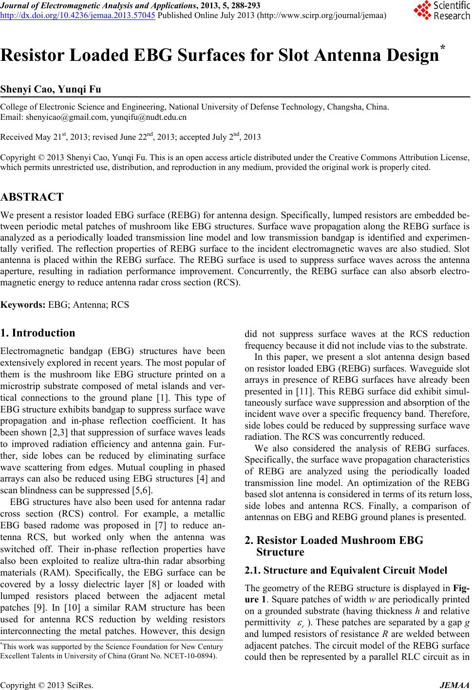
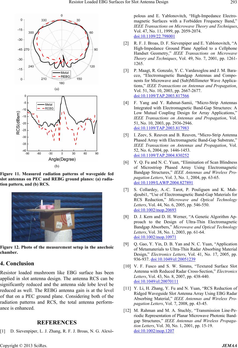
Figure 11. Measured radiation patterns of waveguide fed
slot antennas on PEC and REBG ground planes: (a) radia-
tion pattern, and (b) RCS.
Figure 12. Photo of the measurement setup in the anechoic
chamber.
4. Conclusion
Resistor loaded mushroom like EBG surface has been
applied in slot antenna design. The antenna RCS can be
significantly reduced and the antenna side lobe level be
reduced as well. The REBG antenna gain is at the level
of that on a PEC ground plane. Considering both of the
radiation patterns and RCS, the total antenna perform-
ance is enhanced.
REFERENCES
[1] D. Sievenpiper, L. J. Zhang, R. F. J. Broas, N. G. Alexό-
polous and E. Yablonovitch, “High-Impedance Electro-
magnetic Surfaces with a Forbidden Frequency Band,”
IEEE Transactions on Microwave Theory and Techniques,
Vol. 47, No. 11, 1999, pp. 2059-2074.
doi:10.1109/22.798001
[2] R. F. J. Broas, D. F. Sievenpiper and E. Yablonovitch, “A
High-Impedance Ground Plane Applied to a Cellphone
Handset Geometry,” IEEE Transactions on Microwave
Theory and Techniques, Vol. 49, No. 7, 2001, pp. 1261-
1265.
[3] P. Maagt, R. Gonzalo, Y. C. Vardaxoglou and J. M. Bara-
cco, “Electromagnetic Bandgap Antennas and Compo-
nents for Microwave and (Sub)Millimeter Wave Applica-
tions,” IEEE Transactions on Antennas and Propagation,
Vol. 51, No. 10, 2003, pp. 2667-2677.
doi:10.1109/TAP.2003.817566
[4] F. Yang and Y. Rahmat-Samii, “Micro-Strip Antennas
Integrated with Electromagnetic Band-Gap Structures: A
Low Mutual Coupling Design for Array Applications,”
IEEE Transactions on Antennas and Propagation, Vol.
51, No. 10, 2003, pp. 2936-2946.
doi:10.1109/TAP.2003.817983
[5] I. Zeev, S. Reuven and B. Reuven, “Micro-Strip Antenna
Phased Array with Electromagnetic Band-Gap Substrate,”
IEEE Transactions on Antennas and Propagation, Vol.
52, No. 6, 2004, pp. 1446-1453.
doi:10.1109/TAP.2004.830252
[6] Y. Q. Fu and N. C. Yuan, “Elimination of Scan Blindness
of Microstriop Phased Array Using Electromagnetic
Bandgap Structures,” IEEE Antennas and Wireless Pro-
pagation Letters, Vol. 3, No. 1, 2004, pp. 63-65.
doi:10.1109/LAWP.2004.827891
[7] S. Collardey, A.-C. Tarot, P. Pouliguen and K. Mah-
djoubi1, “Use of Electromagnetic Band-Gap Materials for
RCS Reduction,” Microwave and Optical Technology
Letters, Vol. 44, No. 6, 2005, pp. 546-550.
doi:10.1002/mop.20693
[8] D. J. Kern and D. H. Werner, “A Genetic Algorithm Ap-
proach to the Design of Ultra-Thin Electromagnetic
Bandgap Absorbers,” Microwave and Optical Technology
Letters, Vol. 38, No. 1, 2003, pp. 61-64.
doi:10.1002/mop.10971
[9] Q. Gao, Y. Yin, D. B. Yan and N. C. Yuan, “Application
of Metamaterials to Ultra-Thin Radar Absorbing Material
Design,” Electronics Letters, Vol. 41, No. 17, 2005, pp.
936-937. doi:10.1049/el:20051239
[10] V. F. Fusco and S. W. Simms, “Textured Surface Slot
Antenna with Reduced Radar Cross-Section,” Electronics
Letters, Vol. 43, No. 8, 2007, pp. 438-440.
doi:10.1049/el:20070111
[11] Y. Li, H. Zhang, Y. Fu and N. Yuan, “RCS Reduction of
Ridged Waveguide Slot Antenna Array Using EBG Radar
Absorbing Material,” IEEE Antennas and Wireless Pro-
pagation Letters, Vol. 7, 2008, pp. 43-45.
[12] M. Rahman and M. A. Stuchly, “Transmission Line-Pe-
riodic Representation of Planar Microwave Photonic Band-
gap Structures,” IEEE Antennas and Wireless Propaga-
tion Letters, Vol. 30, No. 1, 2001, pp. 15-19.
doi:10.1002/mop.1207