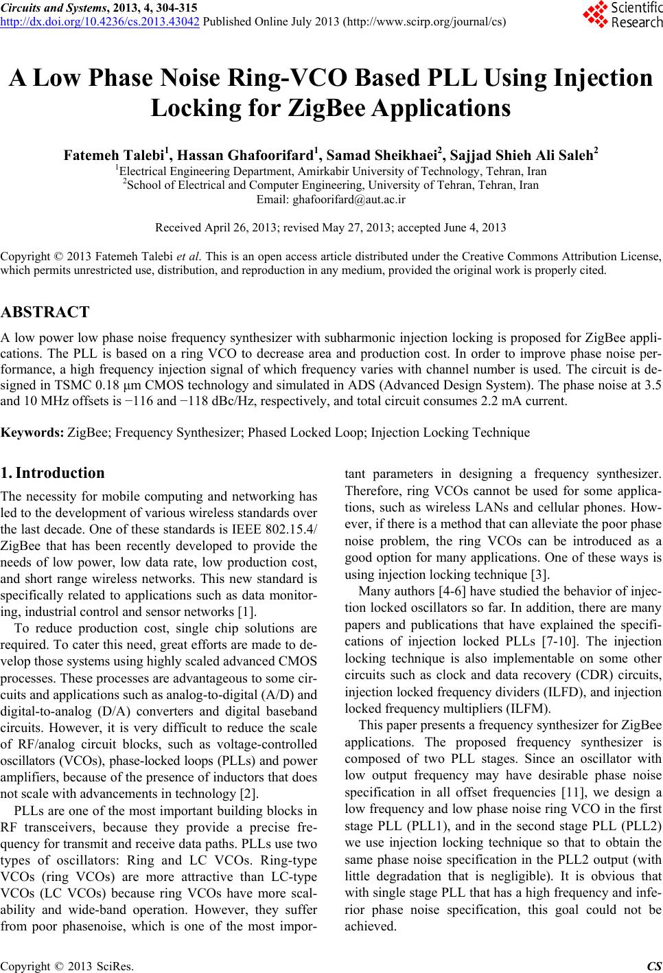
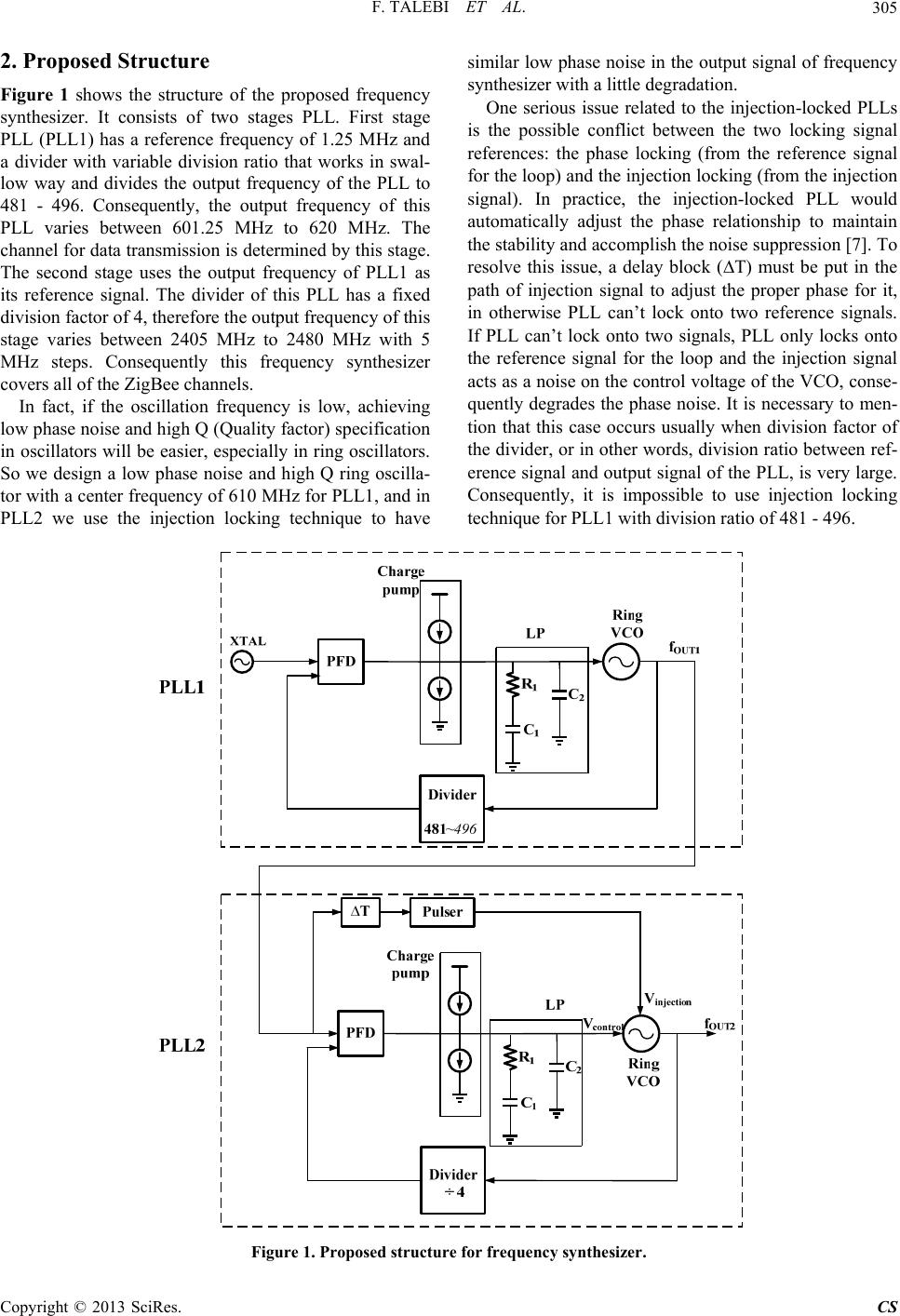
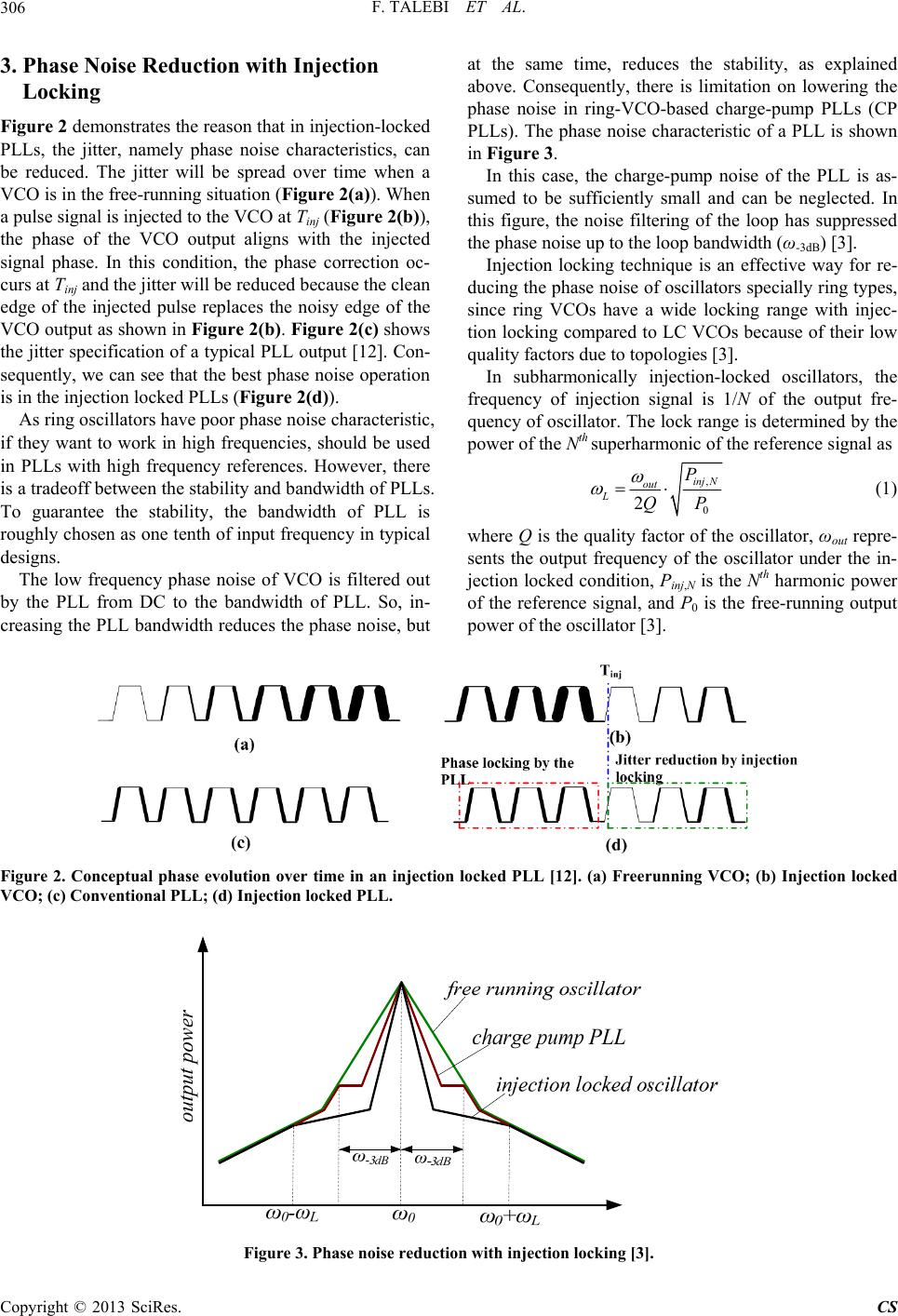
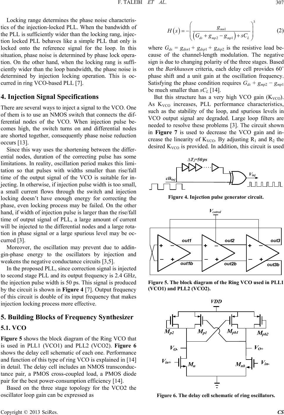
Circuits and Systems, 2013, 4, 304-315
http://dx.doi.org/10.4236/cs.2013.43042 Published Online July 2013 (http://www.scirp.org/journal/cs)
A Low Phase Noise Ring-VCO Based PLL Using Injection
Locking for ZigBee Applications
Fatemeh Talebi1, Hassan Ghafoorifard1, Samad Sheikhaei2, Sajjad Shieh Ali Saleh2
1Electrical Engineering Department, Amirkabir University of Technology, Tehran, Iran
2School of Electrical and Computer Engineering, University of Tehran, Tehran, Iran
Email: ghafoorifard@aut.ac.ir
Received April 26, 2013; revised May 27, 2013; accepted June 4, 2013
Copyright © 2013 Fatemeh Talebi et al. This is an open access article distributed under the Creative Commons Attribution License,
which permits unrestricted use, distribution, and reproduction in any medium, provided the original work is properly cited.
ABSTRACT
A low power low phase noise frequency synthesizer with subharmonic injection locking is proposed for ZigBee appli-
cations. The PLL is based on a ring VCO to decrease area and production cost. In order to improve phase noise per-
formance, a high frequency injection signal of which frequency varies with channel number is used. The circuit is de-
signed in TSMC 0.18 μm CMOS technology and simulated in ADS (Advanced Design System). The phase noise at 3.5
and 10 MHz offsets is 116 and 118 dBc/Hz, respectively, and total circuit consumes 2.2 mA current.
Keywords: ZigBee; Frequency Synthesizer; Phased Locked Loop; Injection Locking Technique
1. Introduction
The necessity for mobile computing and networking has
led to the development of various wireless standards over
the last decade. One of these standards is IEEE 802.15.4/
ZigBee that has been recently developed to provide the
needs of low power, low data rate, low production cost,
and short range wireless networks. This new standard is
specifically related to applications such as data monitor-
ing, industrial control and sensor networks [1].
To reduce production cost, single chip solutions are
required. To cater this need, great efforts are made to de-
velop those systems using highly scaled advanced CMOS
processes. These processes are advantageous to some cir-
cuits and applications such as analog-to-digital (A/D) and
digital-to-analog (D/A) converters and digital baseband
circuits. However, it is very difficult to reduce the scale
of RF/analog circuit blocks, such as voltage-controlled
oscillators (VCOs), phase-locked loops (PLLs) and power
amplifiers, because of the presence of inductors that does
not scale with advancements in technology [2].
PLLs are one of the most important building blocks in
RF transceivers, because they provide a precise fre-
quency for transmit and receive data paths. PLLs use two
types of oscillators: Ring and LC VCOs. Ring-type
VCOs (ring VCOs) are more attractive than LC-type
VCOs (LC VCOs) because ring VCOs have more scal-
ability and wide-band operation. However, they suffer
from poor phasenoise, which is one of the most impor-
tant parameters in designing a frequency synthesizer.
Therefore, ring VCOs cannot be used for some applica-
tions, such as wireless LANs and cellular phones. How-
ever, if there is a method that can alleviate the poor phase
noise problem, the ring VCOs can be introduced as a
good option for many applications. One of these ways is
using injection locking technique [3].
Many authors [4-6] have studied the behavior of injec-
tion locked oscillators so far. In addition, there are many
papers and publications that have explained the specifi-
cations of injection locked PLLs [7-10]. The injection
locking technique is also implementable on some other
circuits such as clock and data recovery (CDR) circuits,
injection locked frequency dividers (ILFD), and injection
locked frequency multipliers (ILFM).
This paper presents a frequency synthesizer for ZigBee
applications. The proposed frequency synthesizer is
composed of two PLL stages. Since an oscillator with
low output frequency may have desirable phase noise
specification in all offset frequencies [11], we design a
low frequency and low phase noise ring VCO in the first
stage PLL (PLL1), and in the second stage PLL (PLL2)
we use injection locking technique so that to obtain the
same phase noise specification in the PLL2 output (with
little degradation that is negligible). It is obvious that
with single stage PLL that has a high frequency and infe-
rior phase noise specification, this goal could not be
achieved.
C
opyright © 2013 SciRes. CS
F. TALEBI ET AL. 305
2. Proposed Structure
Figure 1 shows the structure of the proposed frequency
synthesizer. It consists of two stages PLL. First stage
PLL (PLL1) has a reference frequency of 1.25 MHz and
a divider with variable division ratio that works in swal-
low way and divides the output frequency of the PLL to
481 - 496. Consequently, the output frequency of this
PLL varies between 601.25 MHz to 620 MHz. The
channel for data transmission is determined by this stage.
The second stage uses the output frequency of PLL1 as
its reference signal. The divider of this PLL has a fixed
division factor of 4, therefore the output frequency of this
stage varies between 2405 MHz to 2480 MHz with 5
MHz steps. Consequently this frequency synthesizer
covers all of the ZigBee channels.
In fact, if the oscillation frequency is low, achieving
low phase noise and high Q (Quality factor) specification
in oscillators will be easier, especially in ring oscillators.
So we design a low phase noise and high Q ring oscilla-
tor with a center frequency of 610 MHz for PLL1, and in
PLL2 we use the injection locking technique to have
similar low phase noise in the output signal of frequency
synthesizer with a little degradation.
One serious issue related to the injection-locked PLLs
is the possible conflict between the two locking signal
references: the phase locking (from the reference signal
for the loop) and the injection locking (from the injection
signal). In practice, the injection-locked PLL would
automatically adjust the phase relationship to maintain
the stability and accomplish the noise suppression [7]. To
resolve this issue, a delay block (T) must be put in the
path of injection signal to adjust the proper phase for it,
in otherwise PLL can’t lock onto two reference signals.
If PLL can’t lock onto two signals, PLL only locks onto
the reference signal for the loop and the injection signal
acts as a noise on the control voltage of the VCO, conse-
quently degrades the phase noise. It is necessary to men-
tion that this case occurs usually when division factor of
the divider, or in other words, division ratio between ref-
erence signal and output signal of the PLL, is very large.
Consequently, it is impossible to use injection locking
technique for PLL1 with division ratio of 481 - 496.
Figure 1. Proposed structure for frequency synthesizer.
Copyright © 2013 SciRes. CS
F. TALEBI ET AL.
306
3. Phase Noise Reduction with Injection
Locking
Figure 2 demonstrates the reason that in injection-locked
PLLs, the jitter, namely phase noise characteristics, can
be reduced. The jitter will be spread over time when a
VCO is in the free-running situation (Fig ure 2(a) ). When
a pulse signal is injected to the VCO at Tinj (Figure 2(b)),
the phase of the VCO output aligns with the injected
signal phase. In this condition, the phase correction oc-
curs at Tinj and the jitter will be reduced because the clean
edge of the injected pulse replaces the noisy edge of the
VCO output as shown in Figure 2( b). Figure 2(c) shows
the jitter specification of a typical PLL output [12]. Con-
sequently, we can see that the best phase noise operation
is in the injection locked PLLs (Figure 2 (d)).
As ring oscillators have poor phase noise characteristic,
if they want to work in high frequencies, should be used
in PLLs with high frequency references. However, there
is a tradeoff between the stability and bandwidth of PLLs.
To guarantee the stability, the bandwidth of PLL is
roughly chosen as one tenth of input frequency in typical
designs.
The low frequency phase noise of VCO is filtered out
by the PLL from DC to the bandwidth of PLL. So, in-
creasing the PLL bandwidth reduces the phase noise, but
at the same time, reduces the stability, as explained
above. Consequently, there is limitation on lowering the
phase noise in ring-VCO-based charge-pump PLLs (CP
PLLs). The phase noise characteristic of a PLL is shown
in Figure 3.
In this case, the charge-pump noise of the PLL is as-
sumed to be sufficiently small and can be neglected. In
this figure, the noise filtering of the loop has suppressed
the phase noise up to the loop bandwidth (ω-3dB) [3].
Injection locking technique is an effective way for re-
ducing the phase noise of oscillators specially ring types,
since ring VCOs have a wide locking range with injec-
tion locking compared to LC VCOs because of their low
quality factors due to topologies [3].
In subharmonically injection-locked oscillators, the
frequency of injection signal is 1/N of the output fre-
quency of oscillator. The lock range is determined by the
power of the Nth superharmonic of the reference signal as
,
0
2
inj N
out
L
P
QP
 (1)
where Q is the quality factor of the oscillator, ωout repre-
sents the output frequency of the oscillator under the in-
jection locked condition, Pinj,N is the Nth harmonic power
of the reference signal, and P0 is the free-running output
power of the oscillator [3].
Figure 2. Conceptual phase evolution over time in an injection locked PLL [12]. (a) Freerunning VCO; (b) Injection locked
VCO; (c) Conventional PLL; (d) Injection locked PLL.
Figure 3. Phase noise reduction with injection locking [3].
Copyright © 2013 SciRes. CS
F. TALEBI ET AL. 307
Locking range determines the phase noise characteris-
tics of the injection-locked PLL. When the bandwidth of
the PLL is sufficiently wider than the locking rang, injec-
tion locked PLL behaves like a simple PLL that only is
locked onto the reference signal for the loop. In this
situation, phase noise is determined by phase lock opera-
tion. On the other hand, when the locking rang is suffi-
ciently wider than the loop bandwidth, the phase noise is
determined by injection locking operation. This is oc-
curred in ring VCO-based PLL [7].


4. Injection Signal Specifications
There are several ways to inject a signal to the VCO. One
of them is to use an NMOS switch that connects the dif-
ferential nodes of the VCO. When injection pulse be-
comes high, the switch turns on and differential nodes
are shorted together, consequently phase noise reduction
occurs [13].
Since this way uses the shortening between the differ-
ential nodes, duration of the correcting pulse has some
limitations. In reality, oscillation period makes this limi-
tation so that pulses with widths smaller than rise/fall
time of the output signal of the VCO is suitable for in-
jecting. In otherwise, if injection pulse width is too small,
a small current flows through the switch and injection
locking doesn’t have enough energy for correcting the
phase, even locking process may be failed. On the other
hand, if width of injection pulse is larger than the rise/fall
time of output signal of PLL, a large amount of current
will be injected to the differential nodes and a large rota-
tion in phase signal or a large spurious level may be oc-
curred [3].
Moreover, the oscillation may prevent due to addin-
gin-phase energy to the oscillators by injection and
weakens the negative conductance circuits [3,5].
In the proposed PLL, since correction signal is injected
to second stage PLL and its output frequency is 2.4 GHz,
the injection pulse width is 50 ps. This signal is produced
by the circuit is shown in Figure 4 [7]. Output frequency
of this circuit is double of its input frequency that makes
injection locking process more effective.
5. Building Blocks of Frequency Synthesizer
5.1. VCO
Figure 5 shows the block diagram of the Ring VCO that
is used in PLL1 (VCO1) and PLL2 (VCO2). Figure 6
shows the delay cell schematic of each one. Performance
and function of this type of ring VCO is explained in [14]
in detail. The delay cell includes an NMOS transconduc-
tance pair, a PMOS cross-coupled load, a PMOS diode
pair for the best power-consumption efficiency [14].
Based on the three stage topology for the VCO2 the
oscillator loop gain can be expressed as
3
1
21
mn
ds mpmpL
g
Hs Gg gsC



 

(2)
where Gds = gdsn1 + gdsp1 + gdsp2 is the resistive load be-
cause of the channel-length modulation. The negative
sign is due to changing polarity of the three stages. Based
on the Barkhausen criteria, each delay cell provides 60˚
phase shift and a unit gain at the oscillation frequency.
Satisfying the phase condition requires Gds + gmp2 gmp1
be much smaller than sCL [14].
But this structure has a very high VCO gain (KVCO).
As KVCO increases, PLL performance characteristics,
such as the stability of the loop, and spurious levels in
VCO output signal are degraded. Large loop filters are
needed to resolve these problems [3]. The circuit shown
in Figure 7 is used to decrease the VCO gain and in-
crease the linearity of KVCO. By adjusting R1 and R2 the
desired KVCO is provided. In addition, this circuit is used
Figure 4. Injection pulse generator circ uit.
Figure 5. The block diagram of the Ring VCO used in PLL1
(VCO1) and PLL2 (VCO2).
Figure 6. The delay cell schematic of ring oscillators.
Copyright © 2013 SciRes. CS
F. TALEBI ET AL.
308
to provide the supply voltage (Vctrl) for the VCO.
VCO2 has the same general function of VCO1 except
that it uses a very small capacitor to decrease the oscilla-
tion frequency and improve the phase noise characteris-
tic.
5.2. Phase-Frequency Detector and Charge
Pump
Both of the two stage PLLs, PLL1 and PLL2 use the
phase-frequency detector (PFD) proposed in [15]. This is
a novel PFD that prevents generating the reset signal
when the input phase error is out of the range of [−π, π].
As a result, this PFD eliminates the “blind zone” com-
pletely and so reduces the settling time of the loop [15].
Figure 8 shows the logic schematic of this PFD. It is
an improved model of the classical PFD, that uses two
more OR gates and an additional Start signal in its struc-
ture and its mechanism is explained in [15] completely.
Two stages of PLLs use a simple charge pump that is
introduced in [11]. The circuit of this charge pump is
shown in Figure 9.
Figure 7. The circuit is used to decrease the VCO gain and
increase the linearity of KVCO.
Figure 8. PFD schematic [15].
Figure 9. Charge pump circuit [11].
5.3. Frequency Divider
PLL1 uses a new low power frequency divider proposed
in [16]. This frequency divider consists of a dual modulus
prescaler and a divide-by-64. In order to reduce the power
consumption, Swallow counter has been replaced by a
simple digital circuit [16]. Figure 10 shows the proposed
frequency divider.
Figure 11 shows the dual modulus prescaler and Fig-
ure 12 shows the integrated program and swallow co-
unter of the proposed divider. For more details division
process refer to [16].
It divides the input frequency to 481 - 496 and so cov-
ers all of the ZigBee channels.
PLL2 uses a simple divider with divide ratio of 4 that
is composed of two TSPC D-flip flops. Figure 13 shows
this divider.
6. PLL Design
All of the building blocks of the two PLLs are explained
in the previous sections. This section explains the low
pass filter design. A second order filter is used for the
two stages (the schematic of this filter is shown in Fig-
ure 1). The values of the resistors and capacitors for the
two stage PLLs are:
PLL1: R = 353 k, C1 = 20 pF, C2 = 4 pF.
PLL2: R = 36 k, C1 = 4 pF, C2 = 1.5 pF.
7. Simulation Results
This frequency synthesizer is designed in TSMC 0.18 μm
CMOS technology and simulated in ADS. Simulation
results are presented for channel 12 with frequency of
2.46 GHz. In this condition, PLL1 output frequency is
615 MHz.
Figure 14 shows the spectrum of PLL1 output fre-
quency. The spur rejection at 5 and 10 MHz is 54 and
62.4 dB, respectively that remarkably satisfies ZigBee
specifications remarkably. ZigBee requires at least 13
and 43 dB spur rejection at 5 and 10MHz offsets, re-
spectively. Of course, it is the spur rejection for the first
Copyright © 2013 SciRes. CS
F. TALEBI ET AL. 309
Figure 10. The frequency divider for PLL1 [16].
Figure 11. 7/8 dual modulus prescaler [16].
Figure 12. The integrated program and swallow counter.
Figure 13. The PLL2 divider.
stage PLL, but as second stage has a reference signal
with center frequency of 610 MHz and 1.2 GHz injection
signal, their spurs are occurred at 610 MHz and 1.2 GHz
frequencies and the spurs of the first stage output spec-
trum emerge at the harmonics of these two frequencies,
in other words, roughly at the harmonics of 610 MHz.
Figure 15 shows the phase noise of free running VCO
and PLL1. As depicted in this figure, after frequency
offset of about 1 MHz the phase noise characteristic of
the VCO matches that of the PLL. PLL1 output phase
noise at 1 MHz offset frequency is 106.8 dBc/Hz.
As mentioned before, output signal of the first stage is
used both as the second stage reference signal and as the
injection pulse. Simulation tools such as ADS are not
able to exactly calculate phase noise of injection locked
PLLs. But as PLL2 uses a low Q ring-VCO, it has a wide
locking range with respect to its loop bandwidth. There-
fore, its phase noise characteristic is determined by in-
jection pulse phase noise shape, in other words it works
such as a single VCO with the injection locking condi-
tion. So simulating the single VCO with the injection
locking has a result similar to simulating injection locked
PLL.
For simplicity a single clock source with equivalent
jitter to the output phase noise of PLL1 (rms jitter = 3.6
picoseconds that is calculated by integrating phase noise
over 10 Hz to 100 MHz offset frequencies) is used in-
stead of PLL1 in simulating PLL2. Figure 16 shows
phase noise characteristics of VCO2 with and without
injection. The phase noise at 3.5 and 10 MHz offset fre-
quencies is 116 and 118 dBc/Hz respectively that
shows about 15 dBc/Hz improvement in phase noise at
3.5 MHz offset (without injection locking phase noise at
3.5 MHz offset is 101.5 dB/Hz).
Figure 17 shows the output signal spectrum of PLL2
without injection locking and Figure 18 shows it with
injection locking.
As the reference signal (with 615 MHz frequency) and
injection pulse (with 1.23 GHz frequency) for PLL2 have
high frequency, output signal of frequency synthesizer
has no important spurs at offset frequencies near the
main frequency (at 5 and 10 MHz offsets) and the filters
in the transceiver eliminate these spurs. The general form
of an injection locked PLL output spectrum and its spurs
can be seen in Figure 18 obviously.
Figure 19 shows the Vcont (control voltage) signal for
PLL2 and transient behavior of it. PLL1 has 25 µs and
PLL2 (with injection locking) has 3 µs settling time, so
total frequency synthesizer has 28 µs settling time that
notably provides ZigBee specification.
PLL1 and PLL2 draw 2 mA and 2.2 mA form a 1.8 V
supply, respectively. Therefore, total power consumption
is 7.5 mw for the complete frequency synthesizer.
As frequency synthesizer subsystems such as PFD,
charge pump, LPF, and frequency divider are not sensi-
tive to temperature and process (in this application), and
VCO is the most sensitive subsystem, for testing synthe-
sizer in technology corners, just VCO is simulated. Fig-
ure 20 shows VCO1 behavior in the process corners. As
depicted in this figure, the value of KVCO has a little
change in the four corners, but the frequency has about
20% change in the corners of fast-fast and slow-slow.
These variations are not very important because by vary-
ing Vctrl (i.e., supply voltage) the frequency can be set to
desirable value.
Copyright © 2013 SciRes. CS
F. TALEBI ET AL.
Copyright © 2013 SciRes. CS
310
2 3 4 56 7 8910 11
x 10
8
-120
-100
-80
-60
-40
-20
s pectrum of out put signal
Frequency (Hz )
A m pli tut de (dB )
Figure 14. The spectrum of PLL1 output frequency.
Figure 15. The phase noise of free running VCO1 and P LL1.
F. TALEBI ET AL. 311
10
0
10
1
10
2
10
3
10
4
10
5
10
6
10
7
-150
-100
-50
0
50
100
X: 1e+007
Y: -118.3
P hase Noi se of V CO2(dB c/ Hz )
Frequenc y(Hz )
P has e Nois e(dBc / Hz )
I nj ec ti on Loc ked V CO2
Free Running V CO2
Figure 16. Phase noise characteristics of VCO2 with and without injection.
1.5 22.5 33.5 4
x 10
9
-160
-140
-120
-100
-80
-60
-40
-20
s p ect rum of out put si gnal
Frequenc y (Hz )
Am plitutde ( dB)
Figure 17. The output signal spectrum of PLL2 without injection locking.
Copyright © 2013 SciRes. CS
F. TALEBI ET AL.
Copyright © 2013 SciRes. CS
312
1.5 22.5 33. 5
x 10
9
-120
-110
-100
-90
-80
-70
-60
-50
s pect rum of out put si gnal
Frequency (Hz)
Amplitutde (dB)
Figure 18. The output signal spectrum of PLL2 with injection locking.
0.51.01.52.02.53.03.54.0.0 04.55.0
0.6
0.8
1.0
1.2
1.4
0.4
1.6
time, usec
Vcont, V
Figure 19. The Vcont (control voltage) signal for PLL2.
Figure 21 shows VCO2 behavior in the corners of
technology. As mentioned before about VCO1, in this
case the KVCO2 is almost without change in the technol-
ogy corners and just the values of the frequency at fast-
fast and slow-slow corners vary around 20%. This varia-
tion is compensable by a little change in the supply volt-
age value.
Table 1 demonstrates a performance summery and a
comparison of the proposed frequency synthesizer with
other ZigBee synthesizers. This frequency synthesizer
has similar performance as other synthesizers, but its
most important specification is using a ring oscillator that
F. TALEBI ET AL. 313
11.5 22.5
4.5
5
5.5
6
6.5
7
7.5
8
8.5 x 10
8
Kvco
Control Voltage(v)
Frequency(Hz)
FF
SF
TT
FS
SS
Figure 20. VCO1 behavior in the technology corners.
0.6 0.8 11.2 1.4 1.6 1.8 22.2 2.4
1. 8
2
2. 2
2. 4
2. 6
2. 8
3
3. 2
3. 4
x 10
9
Kvco
Cont rol Vo ltage(v)
Freque ncy (Hz)
FF
SF
TT
FS
SS
Figure 21. VCO2 behavior in the corners of technology.
Copyright © 2013 SciRes. CS
F. TALEBI ET AL.
314
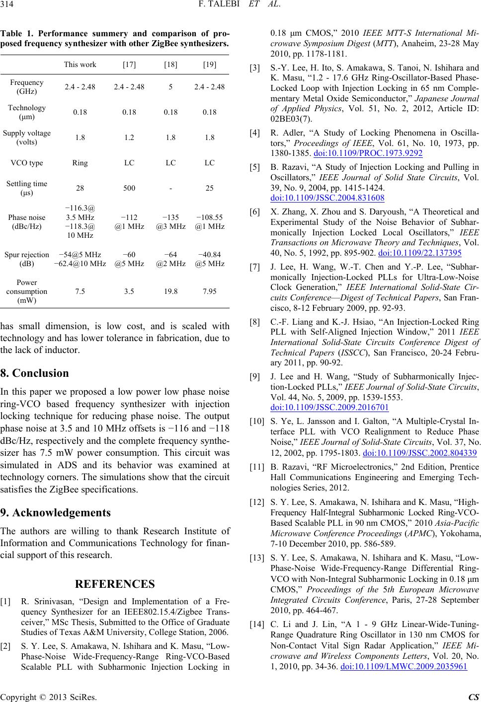
Table 1. Performance summery and comparison of pro-
posed frequency sy nthe sizer with other ZigBee synthesizers.
This work [17] [18] [19]
Frequency
(GHz) 2.4 - 2.48 2.4 - 2.48 5 2.4 - 2.48
Technology
(μm) 0.18 0.18 0.18 0.18
Supply voltage
(volts) 1.8 1.2 1.8 1.8
VCO type Ring LC LC LC
Settling time
(μs) 28 500 - 25
Phase noise
(dBc/Hz)
116.3@
3.5 MHz
118.3@
10 MHz
112
@1 MHz
135
@3 MHz
108.55
@1 MHz
Spur rejection
(dB)
54@5 MHz
62.4@10 MHz
60
@5 MHz
64
@2 MHz
40.84
@5 MHz
Power
consumption
(mW)
7.5 3.5 19.8 7.95
has small dimension, is low cost, and is scaled with
technology and has lower tolerance in fabrication, due to
the lack of inductor.
8. Conclusion
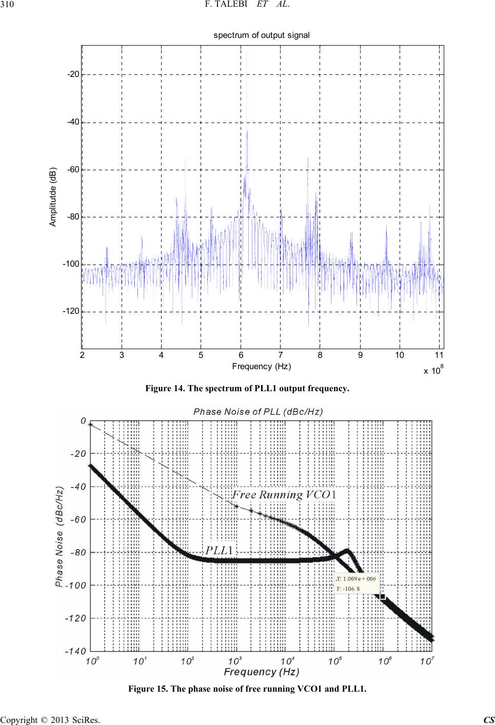
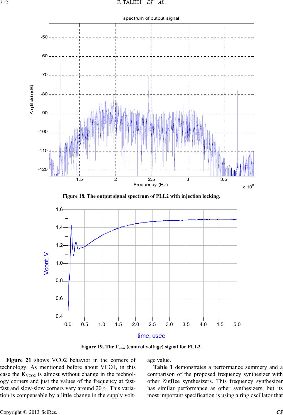
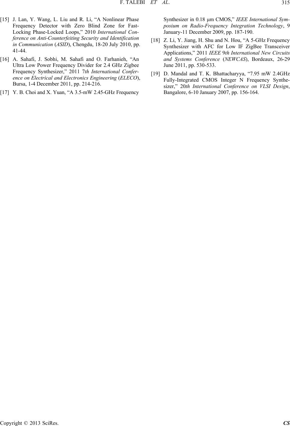
In this paper we proposed a low power low phase noise
ring-VCO based frequency synthesizer with injection
locking technique for reducing phase noise. The output
phase noise at 3.5 and 10 MHz offsets is 116 and 118
dBc/Hz, respectively and the complete frequency synthe-
sizer has 7.5 mW power consumption. This circuit was
simulated in ADS and its behavior was examined at
technology corners. The simulations show that the circuit
satisfies the ZigBee specifications.
9. Acknowledgements
The authors are willing to thank Research Institute of
Information and Communications Technology for finan-
cial support of this research.
REFERENCES
[1] R. Srinivasan, “Design and Implementation of a Fre-
quency Synthesizer for an IEEE802.15.4/Zigbee Trans-
ceiver,” MSc Thesis, Submitted to the Office of Graduate
Studies of Texas A&M University, College Station, 2006.
[2] S. Y. Lee, S. Amakawa, N. Ishihara and K. Masu, “Low-
Phase-Noise Wide-Frequency-Range Ring-VCO-Based
Scalable PLL with Subharmonic Injection Locking in
0.18 μm CMOS,” 2010 IEEE MTT-S International Mi-
crowave Symposium Digest (MTT), Anaheim, 23-28 May
2010, pp. 1178-1181.
[3] S.-Y. Lee, H. Ito, S. Amakawa, S. Tanoi, N. Ishihara and
K. Masu, “1.2 - 17.6 GHz Ring-Oscillator-Based Phase-
Locked Loop with Injection Locking in 65 nm Comple-
mentary Metal Oxide Semiconductor,” Japanese Journal
of Applied Physics, Vol. 51, No. 2, 2012, Article ID:
02BE03(7).
[4] R. Adler, “A Study of Locking Phenomena in Oscilla-
tors,” Proceedings of IEEE, Vol. 61, No. 10, 1973, pp.
1380-1385. doi:10.1109/PROC.1973.9292
[5] B. Razavi, “A Study of Injection Locking and Pulling in
Oscillators,” IEEE Journal of Solid State Circuits, Vol.
39, No. 9, 2004, pp. 1415-1424.
doi:10.1109/JSSC.2004.831608
[6] X. Zhang, X. Zhou and S. Daryoush, “A Theoretical and
Experimental Study of the Noise Behavior of Subhar-
monically Injection Locked Local Oscillators,” IEEE
Transactions on Microwave Theory and Techniques, Vol.
40, No. 5, 1992, pp. 895-902. doi:10.1109/22.137395
[7] J. Lee, H. Wang, W.-T. Chen and Y.-P. Lee, “Subhar-
monically Injection-Locked PLLs for Ultra-Low-Noise
Clock Generation,” IEEE International Solid-State Cir-
cuits ConferenceDigest of Technical Papers, San Fran-
cisco, 8-12 February 2009, pp. 92-93.
[8] C.-F. Liang and K.-J. Hsiao, “An Injection-Locked Ring
PLL with Self-Aligned Injection Window,” 2011 IEEE
International Solid-State Circuits Conference Digest of
Technical Papers (ISSCC), San Francisco, 20-24 Febru-
ary 2011, pp. 90-92.
[9] J. Lee and H. Wang, “Study of Subharmonically Injec-
tion-Locked PLLs,” IEEE Journal of Solid-State Circuits,
Vol. 44, No. 5, 2009, pp. 1539-1553.
doi:10.1109/JSSC.2009.2016701
[10] S. Ye, L. Jansson and I. Galton, “A Multiple-Crystal In-
terface PLL with VCO Realignment to Reduce Phase
Noise,” IEEE Journal of Solid-State Circuits, Vol. 37, No.
12, 2002, pp. 1795-1803. doi:10.1109/JSSC.2002.804339
[11] B. Razavi, “RF Microelectronics,” 2nd Edition, Prentice
Hall Communications Engineering and Emerging Tech-
nologies Series, 2012.
[12] S. Y. Lee, S. Amakawa, N. Ishihara and K. Masu, “High-
Frequency Half-Integral Subharmonic Locked Ring-VCO-
Based Scalable PLL in 90 nm CMOS,” 2010 Asia-Pacific
Microwave Conference Proceedings (APMC), Yokohama,
7-10 December 2010, pp. 586-589.
[13] S. Y. Lee, S. Amakawa, N. Ishihara and K. Masu, “Low-
Phase-Noise Wide-Frequency-Range Differential Ring-
VCO with Non-Integral Subharmonic Locking in 0.18 μm
CMOS,” Proceedings of the 5th European Microwave
Integrated Circuits Conference, Paris, 27-28 September
2010, pp. 464-467.
[14] C. Li and J. Lin, “A 1 - 9 GHz Linear-Wide-Tuning-
Range Quadrature Ring Oscillator in 130 nm CMOS for
Non-Contact Vital Sign Radar Application,” IEEE Mi-
crowave and Wireless Components Letters, Vol. 20, No.
1, 2010, pp. 34-36. doi:10.1109/LMWC.2009.2035961
Copyright © 2013 SciRes. CS
F. TALEBI ET AL. 315
[15] J. Lan, Y. Wang, L. Liu and R. Li, “A Nonlinear Phase
Frequency Detector with Zero Blind Zone for Fast-
Locking Phase-Locked Loops,” 2010 International Con-
ference on Anti-Counterfeiting Security and Identification
in Communication (ASID), Chengdu, 18-20 July 2010, pp.
41-44.
[16] A. Sahafi, J. Sobhi, M. Sahafi and O. Farhanieh, “An
Ultra Low Power Frequency Divider for 2.4 GHz Zigbee
Frequency Synthesizer,” 2011 7th International Confer-
ence on Electrical and Electronics Engineering (ELECO),
Bursa, 1-4 December 2011, pp. 214-216.
[17] Y. B. Choi and X. Yuan, “A 3.5-mW 2.45-GHz Frequency
Synthesizer in 0.18 μm CMOS,” IEEE International Sym-
posium on Radio-Frequency Integration Technology, 9
January-11 December 2009, pp. 187-190.
[18] Z. Li, Y. Jiang, H. Shu and N. Hou, “A 5-GHz Frequency
Synthesizer with AFC for Low IF ZigBee Transceiver
Applications,” 2011 IEEE 9th International New Circuits
and Systems Conference (NEWCA S), Bordeaux, 26-29
June 2011, pp. 530-533.
[19] D. Mandal and T. K. Bhattacharyya, “7.95 mW 2.4GHz
Fully-Integrated CMOS Integer N Frequency Synthe-
sizer,” 20th International Conference on VLSI Design,
Bangalore, 6-10 January 2007, pp. 156-164.
Copyright © 2013 SciRes. CS