Journal of Electromagnetic Analysis and Applications
Vol.07 No.12(2015), Article ID:61818,6 pages
10.4236/jemaa.2015.712032
EMF of Hot Charge Carriers Arising at the p-n-Junction under the Influence of the Microwave Field and Light
Gafur Gulyamov, Muhammadjon Gulomkodirovich Dadamirzaev*, Nosir Yusupjanovich Sharibayev, Ne’matjon Zokirov
Namangan Engineering Pedagogical Institute, Namangan, Uzbekistan

Copyright © 2015 by authors and Scientific Research Publishing Inc.
This work is licensed under the Creative Commons Attribution International License (CC BY).


Received 2 October 2015; accepted 7 December 2015; published 10 December 2015

ABSTRACT
It is shown that the increase in the current of an asymmetric p-n-junction, caused by perturbation of potential barrier height and increasing recombination current in a strong microwave field, is suppressed by light generated photo carriers, leading to the displacement of current-voltage characteristics of p-n-junction into the direction of smaller current values.
Keywords:
hot electrons, the Microwave field, p-n-junction, Light, Photocurrent, generation and recombination Currents

1. Introduction
It is known that when in a non-uniform semiconductor temperature gradient occurs between the edges of the semiconductor thermo EMF will arise. Inhomogeneous concentration of charge carriers in semiconductor can be created artificially, for example by means of lighting. If to heat up one edge of the illuminated region and another left at former temperature, then at the end, the semiconductor EMF arises [1] .
Tautz [2] for the first time has considered this effect, and called it thermal photoelectric effect. Tautz’s experimental measurements have shown that under normal temperature gradient this effect is small, although it can be observed.
However, if to heat up only the charge carriers, by such as a microwave field, it is possible to reach higher temperatures, and hence high values of voltage. This effect was observed by Repshas and Ashmontas [3] , but they got very small voltage values, which they called photo-gradient EMF of hot carriers. This name was used in some cases to refer the bulk photo-emf caused by nonuniform distribution of impurities in semiconductors [3] .
A. I. Veynger et al. [4] [5] theoretically and experimentally examined the current and the EMF of hot carriers in germanium n- and p-type at temperatures of lattice 300 K and 77 K.
It is shown that in weak fields the effect is proportional to the square of the field warming up, and strongly heated field. It was experimentally observed that in strong fields there were saturation and even a decrease of this effect. Furthermore, it was found that the effect was very sensitive to the form of the momentum relaxation time depending on the energy of the carriers and the potential on the surface. Also the variations of the photo-EMF were investigated at the germanium p-n-junction during heating of the carriers. It is shown that the photo-EMF increases with the temperature of the minority carriers. Measurement of photo-EMF on hot carriers is a simple and accurate method of determining the temperature of the hot minority carriers.
The experimental scheme is shown in Figure 1 [4] . The sample was placed in a waveguide and illuminated through a slit in the broad wall of the waveguide. Those portions of the sample that should not have been exposed to light (in particular, contacts), were covered with black paper. This figure also schematically illustrates how the region located along the action of a strong microwave field, and light. As the sample contacts were out of the action of light and the microwave field, the EMF occurring in the semiconductor is determined only by the change in temperature and carrier concentration in the sample. Also changes in photoelectric characteristics of the silicon p-n-junctions have been investigated in a strong microwave field [1] . It is shown that the barrier height of p-n-junction in a strong microwave field and reducing the barrier during the lighting of p-n-junction are proportional to the height of the initial barrier, if the latter is reduced by direct displacement. Near zero bias and at reverse bias, this proportionality will be disturbed due to the influence of the reverse current through the p-n-junction.
A mechanism is proposed to increase the barrier of p-n-junction based on the account of generation-recom- bination processes in space-charge layer. During the experiment, CVC of unilluminated and illuminated p-n- junction were pre-measured without the influence of the microwave field. For one of the samples they are shown in Figure 2 (curves 1 and 2, respectively). Under the influence of the microwave field in the sample an additional impulse EMF arises and the additional pulse current passes through the load. Therefore, the CVC of silicon p-n-junction under the influence of the microwave field were built without illumination (Figure 2, curve 3) and under illumination (Figure 2, curve 4) [1] .
However, in the above-mentioned works current and EMF of asymmetric p-n-junction are not theoretically investigated at simultaneous impact of the microwave field and light.
The aim of this work is a theoretical study of currents and EMF of hot carriers in the asymmetric p-n-junction.
2. Theoretical Study of Currents and EMF of hot Charge Carrier’s asymmetric p-n-Junction under the influence of the microwave field and Light
The average value of the total current passing through the diode consists of the electron and hole currents and defined by the following equation [6] [7] :

Figure 1. Illuminating scheme of the sample in the waveguide: 1― waveguide, 2―sample, 3―light [4] .

Figure 2. CVC p-n-junction under various conditions: 1―without lighting and the microwave field; 2―illuminated without the microwave field; 3―without light in the microwave exposure; 4―illuminated and microwave exposure [1] .
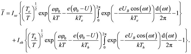 (1)
(1)
where, ;
; ―saturation currents for electrons and holes; j0―the height of the potential barrier in the absence of an electromagnetic wave;
 ; U―a voltage across the diode;
 ―
―
AC voltage the incident wave created by the barrier diode; T is the temperature of the lattice; k―Boltzmann constant; Te, and Th―temperature electrons and holes; Eb―electric field of the wave; e―is the charge of an electron; De and Dh―diffusion coefficients of electrons and holes, Le and Lh―their diffusion length; np and pn― the concentration of minority carriers.
If you do not take into account in the formula (1) heating the charge carriers and the indignation of the potential barrier height (Te = Th = T; UB = 0), we have
 (2)
(2)
This formula is the same as the classic current-voltage characteristic at the p-n-junction as shown in [8] .
After creating the first copper-oxide rectifiers it has been found that when covering the surface of the cuprous light of the appropriate wavelength in the rectifier circuit current starts to flow in the absence of external EMF On this basis we created special devices―photocells barrier layer for converting light into electrical signals.
Copper-ferrous solar cells are not used for energy purposes, as their efficiency is less than a percent. Just after the manufacture of photovoltaic cells for use steel germanium and particularly silicon, it became possible to use solar cells as efficient power converters of sunlight into electrical energy [8] .
As you know, the photocurrent arises only when illuminated by such light, the photon energy is sufficient for the formation of electron-hole pairs, this exceeds the band gap. Light of this wavelength is strongly absorbed, so the pairs are formed near the boundary.
According to (34.16) in [8] , the total current of the photodiode can be written as (where Ic ≠ 0; Te = Th = T; UB = 0)
 , (3)
, (3)
where,  ,
, ―the total loss on the bulk and surface recombination,
 ―relative to the surface recombination losses,
 ―the relative loss of volume recombination,
  , d―the thickness of the illuminated region.
The first term―the so-called dark current, second term―a light current. Equation (3) expresses the additivity rule, according to which the total current is the sum of the photodiode dark current is determined by the applied voltage and is independent of lighting and light current, equal to the number of pairs generated net loss of recombination that does not depend on the applied voltage. In the formula (3) formula expresses generally additive, according to which the total current of the photodiode is equal to the sum of the dark current is determined by the applied voltage and is independent of lighting and light current, equal to the number of generated pairs of net losses on recombination, which is independent of the applied voltage.
According to (1), at low powers the microwave heating can be ignored electrons and holes (when Iс = 0; Te = Th = T; UB ≠ 0), then the current through the diode occurs only as a result, the height of the potential barrier, and it is defined by the formula:
 , (4)
, (4)
where .
.
Using (4) define Thermo photovoltaic current-voltage characteristic at low microwave powers of the wave (when Iс ≠ 0; Te = Th = T; UB ≠ 0):
 (5)
(5)
This shows that you are influenced outrage potential barrier height and light. High power microwave wave (when Iс = 0; Te ≠ Th > T; UB ≠ 0) CVC diode is determined by (1).
Honey CVC p-n-junctions at high power microwave wave (when Iс ≠ 0; Te ≠ Th > T; UB ≠ 0) is determined using (1) as follows:

Figure 3. CVC p-n-junction in the various capacities of the microwave and lighting fittings: 1―without lights and without the microwave field, 2―illuminated and without the microwave field; 3―no lighting and high power microwave energy, 4―at the light and at high power microwave energy.
 (6)
(6)
From these expressions can build CVC p-n-junctions at different conditions. Figure 3 given CVC p-n-junc- tion with the simultaneous action of the microwave and light.
Theoretical graphs (Figure 3) and experimental results (Figure 2) can be compared qualitatively interpretation. Since the concentration distribution of electrons and holes in the p-n-junction [4] is not known, a quantitative comparison of these graphs do not give reliable information about the passage of current through the diode.
3. Conclusion
The theory is developed for the photo-EMF of hot carriers in the p-n-junction in a strong microwave field. An analytical expression is obtained for CVC of illuminated p-n-junction in a strong microwave field. The strong increase of currents of p-n-junction conditioned by the fact that the heating perturbs the height of the potential barrier and increases the recombination currents in the p-n-junction. While lighting increases the generation current in the diode. Since generation and recombination currents are directed oppositely, the illumination of the sample moves the current-voltage characteristics of p-n-junction in the direction of smaller current values. Lighting reduces the overall current flowing through the diode in a strong microwave field. The theoretical results are in qualitative agreement with the experimental results of A. I. Veynger [1] .
Cite this paper
GafurGulyamov,Muhammadjon GulomkodirovichDadamirzaev,Nosir YusupjanovichSharibayev,Ne’matjonZokirov, (2015) EMF of Hot Charge Carriers Arising at the p-n-Junction under the Influence of the Microwave Field and Light. Journal of Electromagnetic Analysis and Applications,07,302-307. doi: 10.4236/jemaa.2015.712032
References
- 1. Ablyazimova, N.A., Veynger, A.I. and Food, V.S. (1992) The Impact of a Strong Microwave Field in the Photovoltaic Properties of Silicon p-n-Junctions. Physics and Engineering of St. Petersburg Semiconductors, 26, 1041-1047.
- 2. Tautz, J. (1962) Photo and Thermoelectric Phenomena in Semiconductors. Moscow, IL, 192s.
- 3. Ashmontas, S.P. (1984) Monograph Series. Electrons in Semiconductors. No. 5. Elektrogradientnye Phenomena in Semiconductors. In: Pozhela, Yu., Ed., Mokslas, Vilnius, 183.
- 4. Veynger, A.I., Kramer, N.I., Paritssky, L.G. and Abdinov, A.S. (1972) Thermophotovoltaic Effect on Heating Carriers in Germany. Semiconductors, 6, 353-359.
- 5. Akopyan, E.A., Veynger, A.I. and Paritssky, L.G. (1974) Photovoltage Hot Carriers at the pn-Junction. Semiconductors, 8, 754-759.
- 6. Dadamirzaev, M.G. (2011) Heating of Charge Carriers and Rectification of Current in Asymmetrical p-n Junction in a Microwave Field. Semiconductors, 45, 288-291.
http://dx.doi.org/10.1134/S1063782611030092 - 7. Dadamirzaev, M.G. (2015) Influence of Deformation on CVC p-n-Junction in a Strong Microwave Field. Journal of Modern Physics-USA, 6, 176-180.
http://dx.doi.org/10.4236/jmp.2015.62023 - 8. Pikus, G.E. (1965) Fundamentals of the Theory of Semiconductor Devices. Science, Moscow, 448.
NOTES

*Corresponding author.