Journal of Electromagnetic Analysis and Applications
Vol.6 No.7(2014), Article
ID:47269,11
pages
DOI:10.4236/jemaa.2014.67016
Ultra-Thin and Flexible Multi-Band Rejection EMI Shield
Lin-Biao Wang1, Jun-Wu Zhang2, Kye Yak See2, Tengiz Svimonishvili2
1Instrumentation and Driver HMI, Continental Automotive Singapore Pte Ltd., Singapore City, Singapore
2School of Electrical and Electronic Engineering, Nanyang Technological University, Singapore City, Singapore
Email: lin.biao.wang@continental-corporation.com, zhan0291@ntu.edu.sg, ekysee@ntu.edu.sg, tengizs@ntu.edu.sg
Copyright © 2014 by authors and Scientific Research Publishing Inc.
This work is licensed under the Creative Commons Attribution International License (CC BY).
http://creativecommons.org/licenses/by/4.0/


Received 31 December 2013; revised 10 February 2014; accepted 15 March 2014
ABSTRACT
This paper presents the design and fabrication of an ultra-thin and flexible electromagnetic interference (EMI) shield that is capable of rejecting multiple unwanted frequencies. The design starts with the equivalent circuit model of periodic concentric rings to determine the initial geometrical dimensions of the rings efficiently. Then it followed by full-wave electromagnetic simulation to fine-tune the final dimensions for the desired frequency response. Impacts of various geometrical designs on the EMI shielding performance of the concentric ring design are analyzed and discussed. With these results, an ultra-thin and flexible EMI shield is fabricated using the screen printing technique. Finally, its multi-band rejection performance is validated experimentally. Good correlation between measurement and simulation is demonstrated in this paper.
Keywords:Frequency Selective Surfaces, Equivalent Circuit Modeling, Full Wave Modeling, EMI Shielding

1. Introduction
With the exponential growth of wireless communications, the number of base stations is expected to increase for better service coverage. As a result, there is a strong likelihood of electromagnetic interference (EMI) from these wireless communications to other sensitive electronic devices. EMI mitigation, such as shielding, has been gaining attention [1] . To protect sensitive equipment from potential EMI threat, there is an increasing demand for architectural shielding. The conventional shielded enclosures are heavy and add structural loadings to existing buildings [2] . Hence, light weight EMI shields that are ultra-thin, highly flexible and can be applied to existing walls of a building will be an attractive solution [3] . Besides the weight issue, conventional metallic enclosures have no frequency selective shielding feature and practically block out electromagnetic waves of all frequencies. For EMI shield that only block out several undesirable frequencies, frequency selective surface (FSS) design maybe applied to offer such capability [4] -[6] . The FSS design also allows void areas to be implemented on the shield, leading to another desirable property, the optical transparency.
There are much reported work on frequency selective structures for various applications and will not be repeated here [7] -[17] . However, it is to be noted that in order to achieve multi-band frequency selective surfaces, cascaded FSSs are usually used. The cascaded nature of the design leads to relatively thick shield [18] -[20] . In order to implement the design onto a single layer, loop design is a good choice [21] [22] . By taking advantage of printed periodic elements to provide the frequency selective feature, the EMI shield can reject specific unwanted frequencies without affecting other wireless services. This paper describes the design procedure of an ultra-thin and flexible multiple-band rejection EMI shield. Screen-printing technique is adopted for the fabrication of the EMI shield because of its roll-by-roll mass production capability. A prototype based on screen-printing is fabricated and its multi-band rejection capability is demonstrated experimentally.
2. Basic Theory
FSSs are periodic structures resonating at specific frequencies and work as either high pass, low pass, band pass or band stop filters. The frequency response depends on its shape, periodic pattern and geometrical dimensions. The periodic structure can be modeled as an array of equivalent inductors and capacitors for ease of interpretation and analysis [23] . This concept was first applied in the analysis of grids by Anderson [24] and subsequently, there are numerous works concerning its use in modelling different structures having straight conductors [25] -[27] .
To achieve multi-band rejection capability with a single layer structure, a ring structure is proposed, as multiple resonances can be created using concentric rings of different radii. Figure 1 shows the geometry of a unit cell and periodic arrays for single and multiple ring designs.
As mentioned earlier, the ring structure is selected as it allows multiple rings to be placed on the same layer. The fundamental resonance for a concentric ring can be estimated with the following equation [5] :
 (1)
(1)
where  is the resonant wavelength,
  is the speed of light in vacuum,
  is the resonant frequency and r is the radius of the ring. For a single ring, its inductance is given by [28] :
 (2)
(2)
where
 (3)
(3)
 is a correction factor to account for the effect of the ground plane,
  is the substrate thickness and w is the width of the ring. With the known inductance and the resonant frequency of the ring structure, its equivalent capacitance can be obtained by [25] :
 (4)
(4)
With the calculated equivalent inductance and capacitance of the ring, the ABCD matrix representation of a ring is shown in Figure 2.
The reflection and transmission coefficients can be determined as follows [29] :
 (5)
(5)
 (6)
(6)
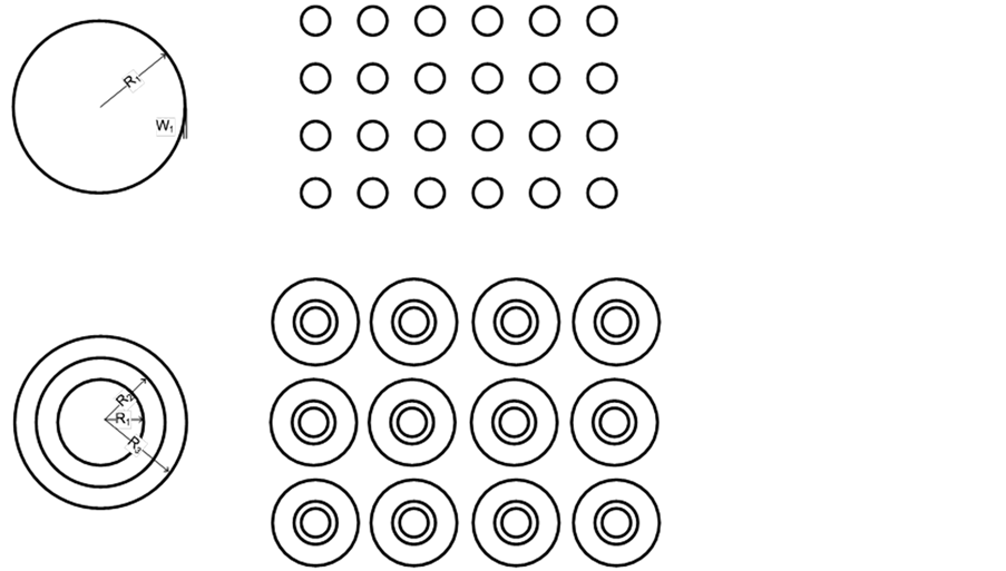
Figure 1. Geometry of a unit cell and periodic array of single-ring and multiple concentric rings.
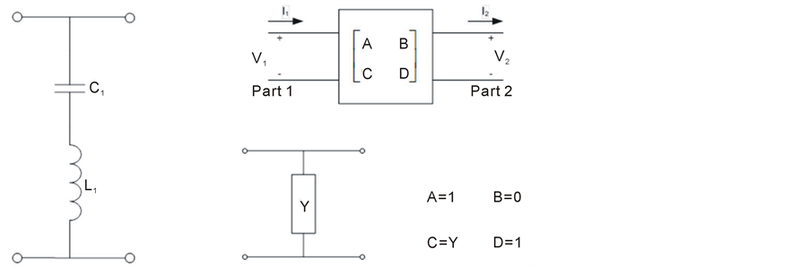
Figure 2. Equivalent circuit and two-port ABCD network representations of single ring.
where , For a shunt network,
  and
and  is the normalized admittance
 . For a series network,
  is the normalized impedance and
 . Equations (5) and (6) allow efficient computation of the transmission and reflection coefficients.
3. Full-Wave Modeling and Analysis
Once the initial geometrical dimensions of the ring structure is obtained from the equivalent circuit model, 3D full wave simulation of the structure can be carried out using a commercial 3D EM solver software with the necessary boundary conditions being considered [30] -[32] . To understand the impacts of various parameters on the rejection performance, the results of different geometrical dimensions are presented in this section.
3.1. Single Ring with Different Radii
Figure 3 and Figure 4 show the full-wave simulated and estimated transmission coefficients for different radii, respectively. It can be seen that the results estimated based on the equivalent circuit model (ECM) resemble well
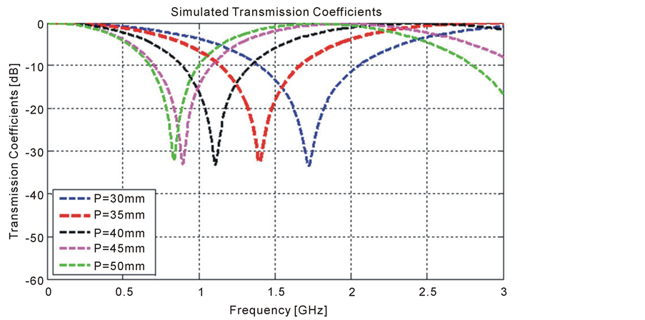
Figure 3. Full-wave simulated transmission coefficients of single ring with varying radii [30, 35, 40, 45 and 50 mm].
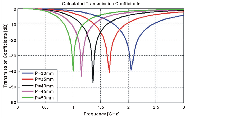
Figure 4. Calculated transmission coefficients of single ring with varying radii using two-port network [30, 35, 40, 45 and 50 mm].
with those simulated using full-wave simulation tool except very slight shift in resonant frequency. However, the ECM approach is highly efficient to synthesize the design quickly without heavy computational effort. This allows parametric analysis to be carried out efficiently as compared to full-wave simulation.
3.2. Single Ring with Varying Substrate Thickness
Figure 5 shows the simulated transmission coefficients for a printed ring on a substrate of thickness ranges from 0.1 mm to 4.0 mm. In the simulation model, the dielectric constant of the substrate is 4 and the radius of the ring is 30 mm. It can be clearly observed that as the resonant frequency shifts downwards with increasing substrate thickness. When the substrate thickness becomes thin enough (h <  /1000), the shift in resonant frequency due to the substrate becomes negligible.
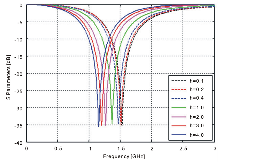
Figure 5. Simulated transmission coefficients of single ring with varying substrate thickness [0.1, 0.2, 0.4, 1.0, 2.0, 3.0 and 4.0 mm].
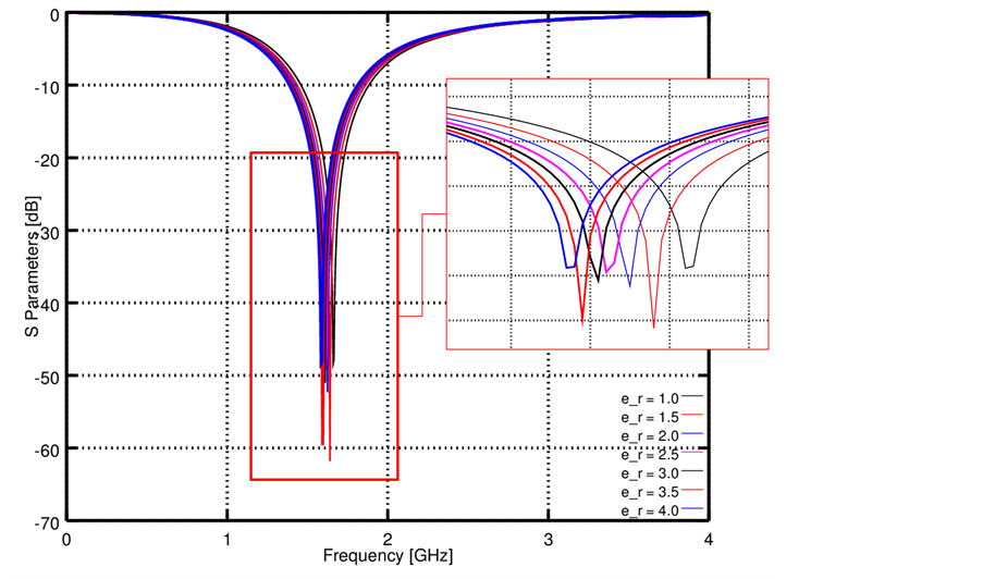
Figure 6. Simulated transmission coefficients of single ring for substrate of varying dielectric constant [ = 1.0, 1.5, 2.0, 2.5, 3.0, 3.5, and 4.0].
3.3. Effect of Substrate Material
To look into the impact of substrate with different dielectric constants, a parametric study is carried out. The radius of the printed ring is kept unchanged at 30 mm and the substrate thickness is also kept at 0.1 mm. A parametric study is carried out with dielectric constant varies from 1 to 4, in steps of 0.5. Figure 6 shows the simulated transmission coefficients for varying dielectric constant.
The simulated results reveal that if the substrate thickness is very thin, the impact of substrate’s dielectric constant on the resonant frequency is minimal.
For the case of a printed ring on one side of a thick substrate, the maximum resonant wavelength is expressed as follows [5] :
 (7)
(7)
It can be included in equations (1)-(7) for the analysis of thick EMI shield. This paper will not dwell into the details, as the focus of this paper is on ultra-thin multi-band rejection EMI shield design.
4. Multi-Band EMI Rejection Shield
To demonstrate an ultra-thin multi-band rejection EMI shield with good optical transmission, this section describes the design of a tri-band EMI shield using concentric rings placed on the same layer. Using the ECM approach discussed in the earlier section, the radii of the printed rings to achieve the three desired frequencies are obtained. With the preliminary geometrical dimensions, further fine-tuning is carried out to achieve the final dimensions for all the resonances to be met on a single-layer design. Table 1 shows the dimensions of the preliminary and final designs. Figure 7 shows the simulated transmission coefficient of the final design after several fine tuning iterations.
For the fabrication of the printed EMI shield, the silver ink is chosen. Its conductivity can be obtained by measurement using a four-point probe technique. The probe is placed in the centre of a fully printed circular pattern. The measured conductivity is founded to be 2.6 × 10⁶ S/m [33] -[35] . Post profile measurement of a circular printed silver disc shows that it has a thickness of 10 µm. The substrate chosen has a dielectric constant of 2.2 with a thickness of 0.1 mm. The electrical properties of both substrate and silver ink are incorporated into the full-wave model to improve the simulation accuracy [36] .
Finally, the tri-band EMI design is realized with screen-printing technique. The key factor behind the use of this process is its ability to print on flexible substrate [37] . Also, the roll-by-roll printing capability makes it an attractive choice for mass production purposes [3] . Being an additive process, it minimizes material wastage. Figure 8 shows the photo of the tri-band rejection EMI shield fabricated by the screen-printing technique.
To validate the tri-band rejection performance of the fabricated EMI shield, a dual horn antenna measurement method proposed in [38] is adopted. Figure 9 shows the experimental setup for characterizing the shielding effectiveness (SE) of the EMI shield. The shield is placed between two horn antennas (EMCO 3115, 1 - 18 GHz). The transmitting and receiving antennas are connected to a vector network analyzer (R & S ZVB8, 300 kHz to 8 GHz) [39] . The adopted method allows SE measurement of planar material without special preparation of edge contacts.
To obtain the SE of the shield, two sets of measurements are to be collected, one with the EMI shield and another without the EMI shield. Once the two measured transmission coefficients are obtained, the SE of the shield can be computed by:

Table 1. Preliminary and final geometrical dimensions of triple concentric rings for tri-band rejection.
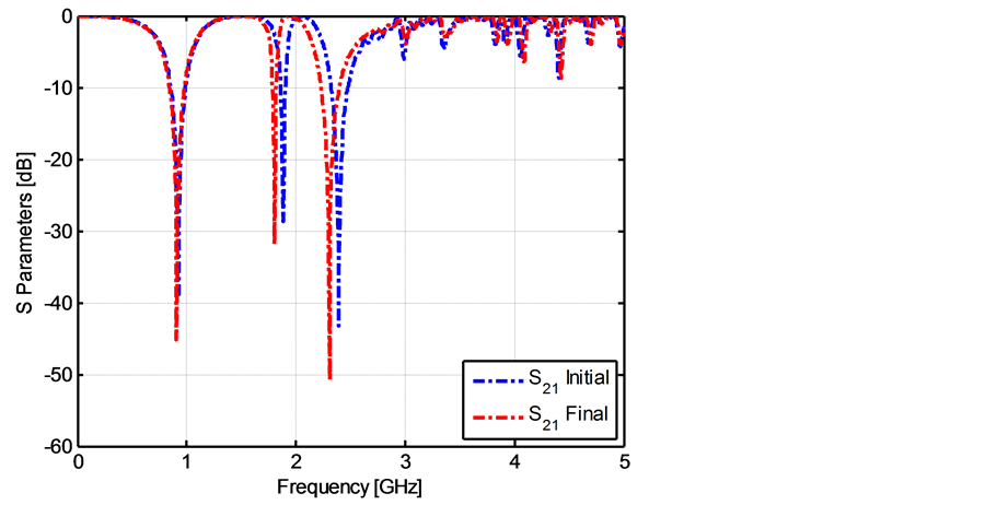
Figure 7. Simulated results of the tri-band rejection EMI shield of preliminary and final designs.
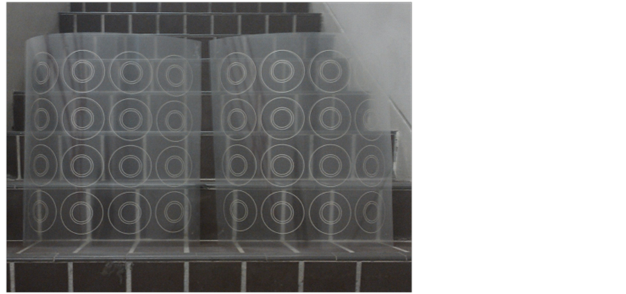
Figure 8. Photo of the fabricated flexible and transparent tri-band rejection EMI shield.
 (8)
(8)
where  and
and  are the measured transmission coefficients without and with the shield, respectively.
To ensure consistency, the shielding performance of the fabricated EMI shield is simulated with the measurement setup included in the model. The dimension of the simulated volume is 350 mm × 350 mm × 1200 mm. In the simulation, absorbing boundary conditions are enforced on all the six faces of the defined volume [40] . Both horn antennas are placed at a distance of 300 mm away from the shield to emulate the actual experimental setup. Figure 10 shows complete simulation model including the EMI shield and the horn antennas.
Taking advantage of plane symmetries helps to reduce the computational effort significant. In the model, two planes of symmetry, y-z plane and x-y plane are exploited. The maximum and minimum grid sizes are 6.7 mm
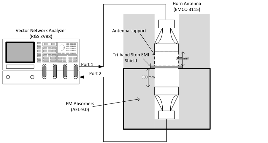
Figure 9. Experimental setup for characterizing the shielding effectiveness of the shield.
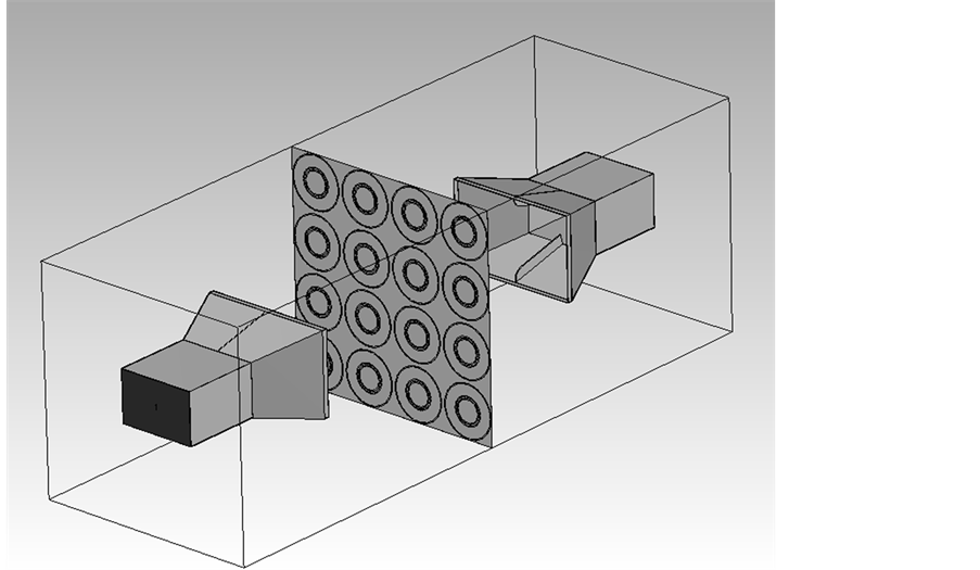
Figure 10. Full-wave simulation model of the fabricated EMI shield including the experimental setup.
and 0.0033 mm, respectively. The substrate thickness (0.1 mm) and its electrical properties ( = 2.2 and
  =1) as well as the silver paste thickness (10 µm) and its electrical properties (
 = 2 ´ 106 S/m and
  = 1) are taken into account for the simulation.
Figure 11 compares the simulated and measured SE of the EMI shield, where the three rejection frequency bands are clearly observed. Good correlation is observed in terms of the resonant frequencies except for the 2.4 GHz band. This is due to finite computing resources. In addition, simulation shows a higher SE as compared to measured SE. This is due to the smaller number of sampling points used during measurement which resulted in a
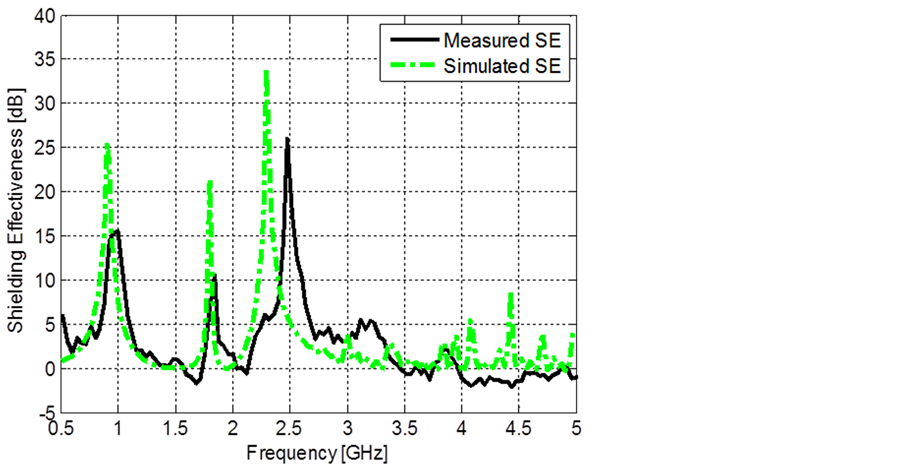
Figure 11. Comparison of simulated and measured SE performance.
less pronounced resonance compared to simulation. Generally, it is demonstrated experimentally that the triband EMI shield is able to provide 16 dB, 11 dB and 27 dB of SE at 900 MHz, 1.8 GHz and 2.45 GHz, respectively.
5. Conclusion
This paper has shown that multi-band rejection EMI shield can be realized based on screen-printing of conductive concentric rings on a single layer, which makes it ultra-thin and highly flexible. The initial design of the EMI shield can be easily established using an efficient equivalent circuit approach and further fine tuning can be achieved with full-wave simulation. Using a tri-band rejection EMI shield as an example, good agreement has been demonstrated experimentally. This kind of EMI shields can be easily applied as wall-paper to existing building walls for rejection of unwanted frequency bands without affecting the desirable frequency bands.
References
- Unal, E., Gokcen, A. and Kutlu, Y. (2006) Effective Electromagnetic Shielding. IEEE Microwave Magazine, 7, 48-54. http://dx.doi.org/10.1109/MMW.2006.1663989
- Hemming, L.H. (1992) Architectural Electromagnetic Shielding Handbook: A Design and Specification Guide. IEEE Press.
- Roll-to-Roll, Flexible, and Multi-Functional. www.simtech.a-star.edu.sg
- Vardaxoglou, J.C. (1997) Frequency Selective Surfaces: Analysis and Design. Wiley, New York.
- Munk, B.A. (2000) Frequency Selective Surface: Design and Theory. Wiley, New York. http://dx.doi.org/10.1002/0471723770
- Celozzi, S., Araneo, R. and Lovat, G. (2008) Electromagnetic Shielding. Wiley-Interscience, Hoboken. http://dx.doi.org/10.1002/9780470268483
- Stefanelli, R. and Trinchero, D. (2009) Scattering Analysis of Frequency Selective Shields for Electromagnetic Indoor Isolation. Microwave Optical Technology Letters, 51, 2758-2762. http://dx.doi.org/10.1002/mop.24739
- Wang, L.B., See, K.Y., Zhang, J.W., Salam, B. and Lu, A.C.W. (2011) Ultra-Thin and Flexible Screen Printed Metasurfaces for EMI Shielding Applications. IEEE Transaction on Electromagnetic Compatibility, 53, 700-705. http://dx.doi.org/10.1109/TEMC.2011.2159509
- Kiani, G.I., Olsson, L.G., Karlsson, A., Esselle, K.P. and Nilsson, M. (2011) Cross-Dipole Bandpass Frequency Selective Surface for Energy-Saving Glass Used in Buildings. IEEE Transactions on Antennas and Propagation, 59, 520-525. http://dx.doi.org/10.1109/TAP.2010.2096382
- Mittra, R., Chan, C.H. and Cwik, T. (1988) Techniques for Analysing Frequency Selective Surfaces—A Review. IEEE Proceedings, 76, 1593-1615.
- Koleck, T., Diez, H. and Bolomey, J.C. (1997) Techniques for Analysing Finite Frequency Selective Surfaces. Antennas and Propagation Conference, 161-165. http://dx.doi.org/10.1049/cp:19970229
- Teo, P.T., Lee, K.S. and Lee, C.K. (2004) Analysis and Design of Band-Pass Frequency-Selective Surfaces Using the FEM CAD Tool. International Journal of RF and Microwave Computer-Aided Engineering, 14, 391-397. http://dx.doi.org/10.1002/mmce.20025
- Cai, Y. and Mias, C. (2006) Time and Frequency Domain Modelling of a Normally Incident Plane Wave at a Periodic Structure. The 6th International Conference on Computational Electromagnetics (CEM), 1-2.
- Savia, S.B. and Parker, E.A. (2003) Equivalent Circuit Model for Superdense Linear Dipole FSS. IEEE Proceedings on Microwave, Antennas and Propagation, 150, 37-42.
- Kent, E.F., Doken, B. and Kartel, M. (2010) A New Equivalent Circuit Based FSS Design Method by Using Genetic Algorithm. International Conference on Engineering Optimization, 1-4.
- Yao, X.Y., Bai, M. and Miao, J.G. (2011) Equivalent Circuit Method for Analyzing Frequency Selective Surface with Ring Patch in Oblique Angles of Incidence. IEEE Antennas and Wireless Propagation Letters, 10, 820-823.http://dx.doi.org/10.1109/LAWP.2011.2164774
- Fernandez, L., Garcia, E., Castro, D. and Segovia, D. (2005) Tool to Design Frequency Selective Surfaces Using an Equivalent Circuit Model. Microwave Technology Letters, 47, 464-467.
- Prakash, V.V.S. and Mittra, R. (2003) Technique for Analysing Cascaded Frequency Selective Surface Screens with Dissimilar Lattice Geometries. IEE Proceedings, Microwave, Antennas and Propagation, 150, 23-27. http://dx.doi.org/10.1049/ip-map:20030436
- Manicoba, R.H.C., Assuncao, D. and Campos, A.L.P.S. (2010) Wide Stop-Band Cascaded Frequency Selective Surfaces with Koch Fractal Elements. The 14th Biennial Electromagnetic Field Computation Conference, May 2010.
- Narayan, S., Pasad, K., Nair, R.U. and Jha, R.M. (2011) A Novel EM Analysis of Cascaded Thick FSS Using Mode-Matching Generalized Scattering Matrix Technique. IEEE Applied Electromagnetics Conference, Kolkata, 18-22 December 2011, 1-4.
- Wu, T.K. and Lee, S.W. (1994) Multiband Frequency Selective Surfaces with Multi-Ring Patch Surfaces. IEEE Transactions on Antennas and Propagation, 42, 1484-1490.
- Kim, D.H. and Choi, J.I. Design of a Multiband Frequency Selective Surface. ETRI Journal, 28, 506-508.
- Marcuvitz, N. (1986) Waveguide Handbook: Peter Penguins Pte Lte.
- Anderson, B.I. (1975) On the Theory of Self-Resonant Grids. The Bell Systems Technical Journal, 54, 1725-1731. http://dx.doi.org/10.1002/j.1538-7305.1975.tb03551.x
- Hamdy, S.M.A. and Parker, E.A. (1982) Comparison of Modal Analysis and Equivalent Circuit Representation of E-Plane Arm of the Jerusalem Cross. Electronics Letters, 18, 94-95. http://dx.doi.org/10.1049/el:19820064
- Langley, R.J. and Parker, E.A. (1982) Equivalent Circuit Model for Arrays of Square Loops. Electronics Letters, 18, 294-296. http://dx.doi.org/10.1049/el:19820201
- Luo, X.F., Teo, P.T., Qing, A. and Lee, C.K. (2005) Design of Double-Square-Loop Frequency-Selective Surfaces Using Differential Evolution Strategy Coupled with Equivalent-Circuit Model. Microwave and Optical Technology Letters, 44, 159-162. http://dx.doi.org/10.1002/mop.20575
- Gupta, K.C., Gurg, R. and Bahl, I.J. (1979) Microstrip Lines and Slot Lines. Artech House, Dedham.
- Pozar, D.M. (1998) Microwave Engineering. 2nd Edition, Wiley, New York.
- www.cst.com
- Ko, W. and Mittra, R. (1993) Implementation of Floquet Boundary Condition in FDTD for FSS Analysis. Antennas and Propagation Society International Symposium, Ann Arbor, 28 June-2 July 1993, 14-17. http://dx.doi.org/10.1109/APS.1993.385413
- Periodic Arrays: FSS/ EBG/ PBG/ LHM, CST Microwave Studio 2006B Application Notes.
- Schroder, D.K. (2006) Semiconductor Material and Device Characterization. IEEE Press.
- Bowler, N. and Huang, Y.Q. (2005) Electrical Conductivity Measurement of Metal Plates Using Broadband Eddy-Current and Four-Point Methods. Measurement Science Technology, 16, 2193-2200.http://dx.doi.org/10.1088/0957-0233/16/11/009
- Electrical Conductivity Measurement of Non-Ferrous Metals Enters a New Dimension. http://www.helmut-fischer.com
- Wang, L.B., See, K.Y., Chang, W.Y., Ng, S.T. and Lu, A.C.W. (2010) Electromagnetic Shielding Analysis of Printed Flexible Meshed Screens. Asia-Pacific Symposium on Electromagnetic Compatibility, Beijing, 12-16 April 2010, 965-968.
- Nakamura, D. (2008) Advanced Screen Printing—Practical Approaches for Printable & Flexible Electronics. International Microsystems, Packaging, Assembly & Circuits Technology Conference, 205-208.
- Marvin, A.C., Dawson, L., Flintoft, I.D. and Dawson, J.F. (2009) A Method for the Measurement of Shielding Effectiveness of Planar Samples Requiring No Sample Edge Preparation or Contact. IEEE Transactions on Electromagnetic Compatibility, 51, 255-262. http://dx.doi.org/10.1109/TEMC.2009.2015147
- R&S®ZVB8 Vector Network Analyzer Datasheet. http://www2.rhode-schwarz.com
- Mur, G. (1981) Absorbing Boundary Conditions for the Finite-Difference Approximation of the Time-Domain Electromagnetic-Field Equations. IEEE Transaction on Electromagnetic Compatibility, EMC-23, 377-382. http://dx.doi.org/10.1109/TEMC.1981.303970