Journal of Electromagnetic Analysis and Applications
Vol. 3 No. 2 (2011) , Article ID: 4122 , 4 pages DOI:10.4236/jemaa.2011.32008
Back to Back Combined Single Feed Proximity Coupled Antenna with Dumbbell Shaped DGS
![]()
Department of Electronics & Computer Engineering, IIT Roorkee, Roorkee, India.
Email: ashwiniarya.iitr@gmail.com, {apatnaik, kartik}@ieee.org
Received November 12th, 2010; revised December 10th, 2010; accepted January 5th, 2011
Keywords: Defected ground structure, Microstrip Antennas, Proximity coupling
ABSTRACT
Use of defected ground structure (DGS) to reduce the size of patch antenna is presented in this paper. In order to get a dipole like radiation pattern for some specific application a dumbbell shaped DGS is used in the common ground plane of back to back combined single fed proximity coupled antenna. A size reduction of about 60% is achieved. Parametric analysis has been done to see the resonance behavior of the antenna with DGS.
1. Introduction
The continuous shrinking size of electronic equipments demands similar size antenna elements in order to fit properly in wireless devices without compromising the other radiation properties of the antenna. In this respect microstrip patch antennas are quite an obvious choice because of its other benefits like low profile, light weight, low cost and easy fabrication.
But as far as size of these patches concerned, the patch length should be around half-a-wavelength for the structure to act as a good radiator. Different techniques have already been used for the antenna size reduction such as using the substrate with high dielectric constant [1] , edge shorted patches with shorting plates or shorting walls, use of the shorting pin at the suitable position etc [2,3].
As far as our understanding goes much has not been reported regarding the use of DGS for size reduction of microstrip antennas, although its application have been reported for harmonic reduction [4], cross-polarization suppression [5] and mutual coupling reduction [6] in antenna arrays etc. Although the back to back geometries have been reported by the various researchers [7,8] but here a new coupling method i.e. proximity coupling with the defected ground structure is used for the consideration of the increased bandwidth.
This paper presents the application of DGS for size reduction of microstrip antennas. A dumbbell shaped DGS is used in the common ground plane of a back to back combined single feed proximity coupled microstrip antenna.
2. Defected Ground Structure
Recently there has been an increasing interest in the use of DGSs for performance enhancement of microstrip antennas and arrays. These are realized by etching off a simple shape defect from the ground plane of the planer circuits.
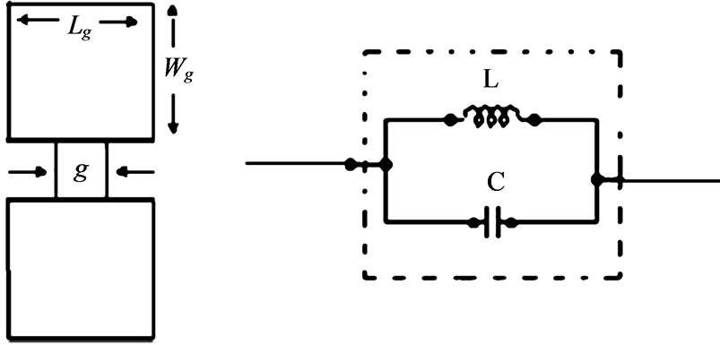
Although various complicated DGSs were reported in the literature, but the simplest one is the dumbbell shaped DGS. Figure 1(a) shows the simple and mostly used dumbbell shaped DGS that is etched in the ground plane below the microstrip line, in which both the areas (Lg*Wg) and the slot gap (g) play a very important role to find the resonance behavior of the DGS.
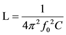
The head areas (Lg*Wg) is very useful for the variation in the inductance (L) and the slot (g) produces the capacitance (C). The L and C may be calculated from the formulae given below [9].
 (a) (b)
Figure 1. (a) Dumbbell shaped DGS, and (b) DGS Equivalent Circuit.
 (1)
(1)
 (2)
(2)
When this DGS is applied to the antenna, the equivalent inductive part due to the DGS increases and produces equivalently the high effective dielectric constant, thereby decreasing the resonant frequency when the DGS is incorporated in the ground plane of a micro strip antenna.
3. Antenna Design with DGS
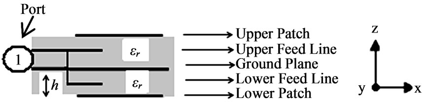
In this section, the design approach and the performance of the basic antenna and the antenna with DGS is described. At the outset, the single patch antenna was designed and simulated using the CST Microwave studio [10], for the operating frequency at 5.0 GHz. Then another patch of the same size was added in the opposite side of the ground plane and fed in the same way as the first one. The configuration seems as two patch antennas having a common ground plane working at the same frequency. Next the feed lines were combined for the antenna for single feed design. For this purpose the antenna feed lines Wf = 0.934 mm with df = 1.5 mm were designed of 100 ohm and for matching to the 50 ohm transmission line (Wp = 3.86 mm) a quarter wave length transformer (Wt = 2 mm) was used to give proper matching (Figure 2).
The cross-sectional view of the single fed back to back combined proximity coupled antenna is shown in the Figure 2(a). The layouts of matching networks only are emphasized in this Figure 2(b) for convenience. It is observed that the antenna designed in this configuration gives the bandwidth of 137 MHz whereas single antenna gives a bandwidth of 67 MHz. This is due to the fact that as the antenna height increases the quality factor decreases and the bandwidth increases. This becomes a multilayer antenna with more height and higher bandwidth as compared to the single patch antenna.
The simple transmission line model was used for the antenna size calculation. The dielectric constant was taken as 3.38 with the loss tangent 0.0025 and of 1.524 mm thickness. The patch lengths Lp and widths Wp are 15 mm and 19 mm respectively. The feed line has been inserted inside the dielectric at a height equal to the half of the height (h = 3.048 mm) of the antenna on either side. The dumbbell shaped DGS with dimensions Lg = Wg = 8.6 mm and g = 0.76 mm was created in the ground plane of the antenna as shown in the Figure 2(c). A small slot was also created for making the antenna with single feed. The two feed lines were connected with a metal strip which goes through the small slot in the ground plane. The fabricated antenna is shown in figure 2(d).
 (a)
(a)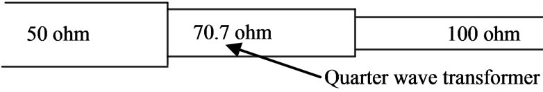 (b)
(b)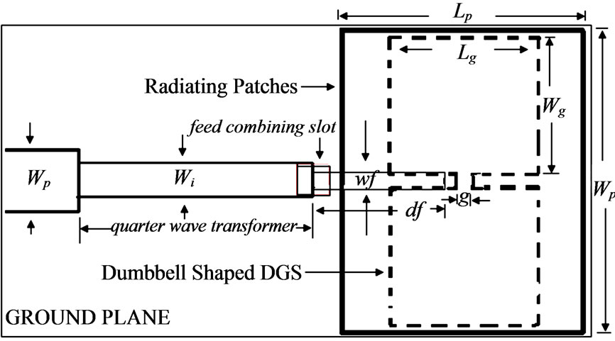 (c)
(c) (d)
(d)
Figure 2. (a) Cross-sectional view of antenna configuration, (b) Feeding Network, (c) Top-View of the antenna, (d) Fabricated Antenna.
4. Results and Discussion
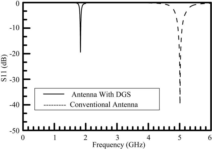
At first the antenna without the DGS in the common ground was simulated and was found to resonate at 5 GHz with 137 MHz Bandwidth.
Then the structure was simulated with the dumbbell shaped DGS. Before reaching to the final size of the DGS, a parametric study was done by varying Lg, Wg and g of the DGS. As shown in Figure 3, with the increase in the value of Lg, the resonant frequency of the antenna is decreasing. Infect, increase in the length of the DGS head gives increasing inductance which in turn decreases the resonant frequency of the antenna.
At this point the increment in the (g) was not possible due to the accuracy in fabrication, so for this reason the other dimension (g) was kept constant for the requirement of the desired frequency (2 GHz). The size of the DGS single square head for the antenna to resonate at 2 GHz (UHF Band) was found to be 8.6 mm × 8.6 mm. The return loss (S11 [dB]) plot of the structure with and without DGS is shown in Figure 4(a). Figure 4(b) shows the measured S11 parameter using the HP 8720 B network analyzer. The marker’s position near to peak shows the resonance frequency 2.08 GHz with return loss of -13 dB. The result shows good agreement with the simulation results. The measured -10 dB bandwidth is about 60 MHz. The maximum size reduction achieved is about 60%.
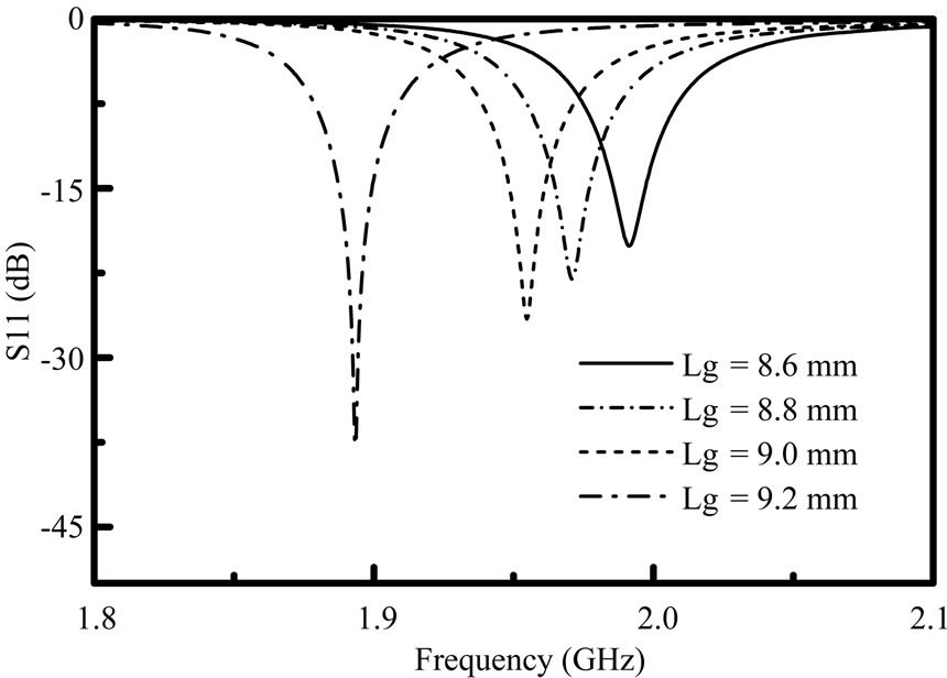
Figure 3. S11 Vs. Frequency response by varying DGS length (Lg).
 (a)
(a)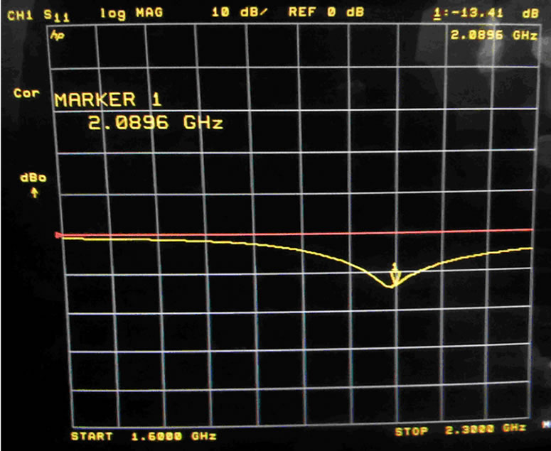 (b)
(b)
Figure 4. Antenna Return Loss (a) simulated (b) measured.
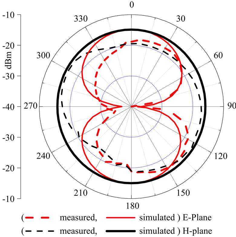
Figure 5. Antenna radiation pattern (measured and simulated) at 2 GHz Frequency.
The measured and simulated power patterns of the antenna are shown in Figure 5. It can be observed that the E-plane radiation pattern is similar to the pattern for a dipole antenna. Measurement errors are mainly due to the spurious radiation created by the feeding end and the improper coupling of the elements. However the gain measured experimentally for the proposed antennas with DGS is about -6.9 dB and -7.8 dB (where simulated gain with DGS is 3.8 dB and 5.7 dB is for the antenna without DGS, for both the planes) in both the E and H plane respectively, which is consistent with the size reduction of the antenna.
5. Conclusion
Microstrip patch antenna size reduction with DGS is carried out in this work. A dumbbell shaped DGS in the common ground plane of a back to back microstrip structure was found to give a size reduction of about 60% and shifts the resonance frequency from 5 GHz to 2 GHz, with 60 MHz bandwidth facilitating the antenna, to be used for UHF band applications.
REFERENCES
- R. Garg, P. Bhartia, I. Bahl and A. Ittipiboon, “Microstrip Antenna Design Handbook,” Artech House, London, 1995.
- P. Salon, M. Keskilammi and M. Kivikoski, “Single Feed Dual Band Planer Inverted-F Antenna with U-Shaped Slot,” IEEE Transactions on Antenna and Propagation, Vol. 48, No. 8, 2000, pp. 1262-1264. doi:10.1109/8.884498
- D.Nashhat, H. Elsadek and H. Ghali, “Dual-Band Reduced Size PIFA Antenna with U-Slot for Bluetooth and WLAN Applications,” Proceedings of IEEE Antennas Propagation International Symposium, Columbus, Vol. 2, 22-27 June 2003, pp. 962-965. doi. 10.1109/APS.2003.1219395
- H. Liu, X. Sun and J. Mao, “Harmonic Suppression with Photonic Bandgap and Defected Ground Structure for a Microstrip Patch Antenna,” IEEE Microwave and Wireless Component Letters, Vol. 15, No. 2, February 2005, pp. 55-56. doi:10.1109/LMWC.2004.842809
- D. Guha, M. Biswas and Y. M. M. Antar, “Microstrip Patch Antenna with Defected Ground Structure for Cross Polarization Suppression,” IEEE Antenna and Wireless Propagation Letter, Vol. 4, No. 1, 2005, pp. 455-458. doi:10.1109/LAWP.2005.860211
- M. Salehi, A. Motevasselian, A. Tavakoli and T. Heidari, “Mutual Coupling Reduction of Microstrip Antenna using Defected Ground Structure,” IEEE Singapore International Conference on Communication System, Singapore, 2006, pp. 1-5. doi:10.1109/ICCS.2006.301375
- J. Guterman, Y. R. Samii, A. A. Moreira and C. Peixeiro, “Quasi-Omni Directional Dual-band Back-to-Back Eshaped Patch Antenna for Laptop Applications,” Electronics Letters, vol. 42, No. 15, 2006, pp. 845-847. doi:10.1049/el:20061799
- H. Iwasaki, “A Back-to-Back Rectangular-Patch Antenna Fed by a CPW,” IEEE Transactions on Antenna Propagation, Vol. 46, No. 10, October 1998, pp. 1527-1530. doi:10.1109/8.725285
- D. Ahn, J. S. Park, C. S. Kim, J. Kim, Y. Qian and T. Itoh, “A Design of the Low-Pass Filter Using The Novel Micro strip Defected Ground Structure,” IEEE Transactions on Microwave Theory and Technology, Vol. 49, No. 1, 2001, pp. 86-91. doi:10.1109/22.899965
- EM Simulation Software CST Studio Suite™, v9.