Materials Sciences and Applications
Vol. 4 No. 5A (2013) , Article ID: 31618 , 9 pages DOI:10.4236/msa.2013.45A003
Hexagonal Nano-Crystalline BCN Films Grown on Si (100) Substrate Studied by X-Ray Absorption Spectroscopy
![]()
1Department of Chemistry and Applied Chemistry, Faculty of Science and Engineering, Saga University, Saga, Japan; 2Synchrotron Radiation Research Unit, Quantum Beam Science Directorate, Japan Atomic Energy Agency, Ibaraki, Japan.
Email: *mannan.chem@ru.ac.bd
Copyright © 2013 Md. Abdul Mannan et al. This is an open access article distributed under the Creative Commons Attribution License, which permits unrestricted use, distribution, and reproduction in any medium, provided the original work is properly cited.
Received January 24th, 2013; revised March 18th, 2013; accepted April 9th, 2013
Keywords: Nano-crystalline; h-BCN films; Synchrotron radiation; XPS; NEXAFS; Orientation
ABSTRACT
Hexagonal nano-crystalline boron carbonitride (h-BCN) films grown on Si (100) substrate have been precisely investigated. The films were synthesized by radio frequency plasma enhanced chemical vapor deposition using tris-dimethylamino borane as a single-source molecular precursor. The deposition was performed by setting RF power at 400 - 800 W. The reaction pressure was at 2.6 Pa and the substrate temperature was recorded at 700˚C - 800˚C. Formation of the nano-crystalline h-BCN compound has been confirmed by X-ray diffraction analysis. The diffraction peaks at 26.3˚ together with a small unknown peak at 29.2˚ were elucidated due to the formation of an h-BCN structure. The films composed of B, C, and N atoms with different B-N, B-C, C-N chemical bonds in forming the sp2-BCN atomic configuration studied by X-ray photoelectron spectroscopy. Orientation and local structures of the h-BCN hybrid were studied by near-edge X-ray absorption fine structure (NEXAFS) measurements. The dominant presence of p* and s* resonance peaks of the sp2-hybrid orbitals in the B K-edge NEXAFS spectra revealed the formation of the sp2-BCN configuration around B atoms like-BN3 in h-BN. The orientation was suggested on the basis of the polarization dependence of B K-edge and N K-edge of the NEXAFS spectra.
1. Introduction
It has been revealed that the hexagonal boron nitride (h-BN) and the graphite have almost isoelectronic structure but physicochemical properties of these two compounds are quite different: the h-BN is an insulator while the graphite is a semiconductor [1]. The isogeometric and isoelectronic structures of the h-BN and graphite have been suggested the possible formation of their solid solution which should have semi-conducting properties and tunable band gap depending on composition [2]. Much effort has been devoted to synthesize of the ternary BCN compounds since they are attractive as super-hard and/or semi-conducting materials with adjustable band gap energy [3,4]. Recently, efforts have been aimed to synthesize single phase of crystalline cubic (c-BCN) and/or hexagonal (h-BCN) boron carbonitride compounds. The c-BCN is expected to be super-hard material comparable to that of diamond and the h-BCN is attractive in the applications to electronic, optical and luminescent devices [5]. The h-BCN could also be applicable to the rechargeable lithium ion battery [6]. Syntheses of the ternary BCN compounds with various compositions by different methods using different source materials have been reported. So far, most of the reported BCN compounds are mixture of nano-crystalline hexagonal and cubic phases or amorphous phase [7-12]. X-ray photoelectron spectroscopy (XPS) has been used for the characterization of the B-C-N hybrids. But most of the XP spectra of the B-C-N hybrids show relatively high content of BN. In addition, the broad features of these spectra suggest that various kinds of B-C-N bonds are included in the hybrid instead of single-phase structure.
Ulrich [13] and Filonenko et al. [14] have tried to deposit c-BCN crystal with different compositions. Single phase of the h-BCN and/or the c-BCN with large grain size has not been synthesized yet and efforts were not devoted to clarify the orientation precisely in the BCN hybrid. However, preparation of single-phase of the hBCN with large grain size is still a challenge because of the difficulty in synthesis with controlled composition.
In our previous study, we reported BCN hybrid films synthesized on Si (100) using TDMAB as the precursor [15,16]. In those reports, the crystalline phase was not detected probably due to the short-range order of the atomic arrangement and/or the amorphous phase. We also synthesized h-BCN hybrid on Si (100) using borane triethylamine (BTEA) complex as the precursor in CH4 + H2 carrier gas [17]. The stoichiometric growth of BCN on HOPG substrate was explored; in addition, we examined the orientation of crystalline h-BCN hybrid on Ni (111) and polycrystalline Ti substrates [18,19].
Since near-edge-X-ray absorption fine structure (NEX AFS) is a unique instrumental method that could be used to clarify the geometrical and orientation of the element in h-BCN hybrid if linearly polarized synchrotron radiation is used. In this paper, we present nanocrystalline h-BCN hybrid compound grown on Si (100) substrate and orientation of the hybrid examined by NEXAFS measurements.
2. Experimental Methods
BCN films have been synthesized on Si (100) by RFPECVD using TDMAB (99% Aldrich) as a single-source molecular precursor. The deposition system has been reported in the reference [16]. The reaction chamber was evacuated up to 1 ´ 10−3 Pa and then the chamber was filled with hydrogen gas (99.99%, Iwatani Co., Japan) without further purification to a desired reaction pressure. The H2 was allowed to flow through a bubbler, containing the precursor material, to the reaction chamber for about 30 min in order to expel the atmospheric oxygen that might cause possible contamination of the films during deposition. Since the precursor is volatile, the vapor was produced by bubbling without decomposition and was allowed to introduce in the reaction system. The flow rate of the H2 was controlled by a mass flow controller (MKS, Type 122A) at 30 sccm. The flow rate of the evaporated TDMAB was controlled by a valve at ~2 sccm. The substrate was placed at the center of the work coil and then the deposition was performed at the RF powers of 400 to 800 W for 30 min at the reaction pressure of 2.6 Pa. The substrate was cleaned by ultrasonic cleaner in acetone followed by hydrofluoric acid (50%). Substrate temperature was controlled by setting the substrate at 1.5 cm upstream from centre of work coil in plasma of the RF generator [16]. The temperature was measured by an optical pyrometer (Model, IR-U CHINO) during deposition. The other deposition parameters are summarized in Table 1. The crystallinity of the as-deposited films was investigated by an X-ray diffractometry (XRD) (Rigaku diffractometer) using Cu Ka radiation (30 kV, 20 mA).
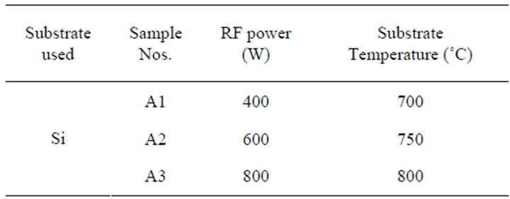
Table 1. Deposition conditions of the samples synthesized on Si (100) substrate (flow rate of the carrier gas = 30 sccm).
The chemical composition and the atomic arrangement were studied by X-ray photoelectron spectroscopy (XPS) and near-edge X-ray absorption fine structure (NEXAFS) measurements. The ex situ XPS and NEXAFS measurements were performed at the Beam Line 11A (BL-11A) and the Beam Line 27A (BL-27A) of the Photon Factory at the High Energy Accelerator Research Organization (KEK), Tsukuba, Japan, using linearly polarized synchrotron radiation (SR) as an excitation source. The XPS measurement was done by using the SR beam of an energy . The space-charge effect was minimized by a flood gun of electrons during the XPS measurements. For further calibration, several spots of gold
  were deposited by a DC magnetron sputtering method on all the individual samples prior to the XPS measurement. The sample surface was not sputtered by Ar+ ion since it may cause some effect on composition. The B1s, C1s, and N1s binding energies for the individual samples were calibrated by Au4f7/2 photoelectron peak (84.0 eV). The elemental composition of B, C, and N was estimated from
  , where I is the intensity of the photoelectron peak and s is the photoionization cross-section for the respective core-level indicated as subscript. The values of s at
  calculated from the data sheet are
 and
and  barns for B1s, C1s, and N1s, respectively [20].
NEXAFS spectra were measured at the BL-11A using a 300 l/mm laminar grating in an UHV chamber  with the total electron yield mode by recording the sample current. NEXAFS spectrum of the pyrolytic h-BN (99%, Wako Chemical Industries, Japan), was measured as a standard. The photon energy of p* resonance of B K-edge for the h-BN was estimated at 191.9 eV which was consistent with the reported values from 191.8 to 192.2 eV [20-22]. In the NEXAFS analyses, the X-ray incidence angle q was defined as the angle between the electric field vector of the linearly polarized X-ray beam and the surface normal of the film [23]. The film thickness was estimated from the cross-section image of the filed emission scanning electron microscopy (FE-SEM) (JSM-6700 FSS, JEOL) observation. The thickness obtained from the cross section image was found to be around 10 mm for the studied samples in this paper.
The Raman spectra of the samples were obtained with a SpectraPro 2300i imaging spectrograph (Acton Research Corporation) equipped with a liquid nitrogen cooled charge-coupled devices (Spec-10:256E, Roper Scientific). The samples were excited with 532 nm Ar+ ion laser and a back scattered light was collected by collection optics. All Raman spectra were measured in backscattering mode at room temperature with the laser power of about 40 mW.
3. Results and Discussion
3.1. XRD Analyses
XRD patterns of the samples are shown in Figure 1. XRD patterns for the h-BN and HOPG are also shown in this figure as reference. The peak observed at 26.3˚ in the diffraction pattern seemingly suggests formation of crystalline structure in these films. The (002) diffraction peak for h-BN and graphite are reported at 2q = 26.8˚ (d = 3.42 Å) and at 2q = 26.6˚ (d = 3.36 Å), respectively and the maximum reflection should be varied from 25.0˚ to 26.3˚ depending on C concentration in the BCN films [24]. Therefore, the peak at 26.3˚ (d = 3.48 - 3.50 Å) could be ascribed in forming crystalline h-BCN phase. The assignment of the h-BCN phase has been supported by NEXAFS spectroscopy described in the following section. The larger interplanar distance as compared with the h-BN and graphite suggests that the h-BCN basal
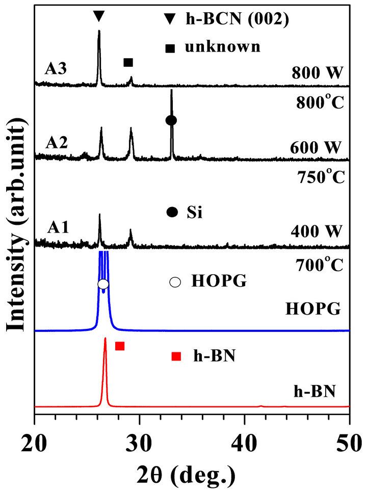
Figure 1. XRD patterns of the samples synthesized on Si (100) substrate at different substrate temperature. XRD patterns for the h-BN and HOPG are also shown at the bottom of the figure for reference. The XRD peaks corresponds to the substrate Si, and HOPG are defined by ●, and O, respectively.
planes are packed rougher than the h-BN and graphite because of ternary atomic mixing of B, C, and N atoms in the sp2 basal plane. The (002) peak was stronger for the samples synthesized at 800˚C. It means that the crystallinity might be improved with temperature. An unknown peak observed at 2q = 29.2˚ (d = 3.16 Å) has not been reported yet for BCN compounds. Since the unknown peak was observed for all these samples, therefore, the unknown peak might also be ascribed to a crystalline BCN phase with small oxide structure though more studies to be needed to clearly identify origin of this peak.
3.2. XPS Analyses
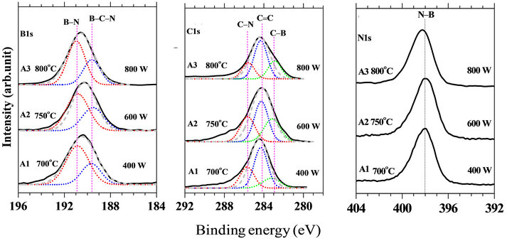
Figures 2(a)-(c) shows B1s, C1s, and N1s XPS spectra for the samples shown in Figure 1. The elemental compositions (at%) of the as-deposited individual samples estimated from XPS wide scan spectra are summarized in Table 2. It has been observed that composition of these films was changed appreciably with the substrate temperature as well as with the RF power used. It has been observed that the B and N concentration increased while the C concentration decreased with the substrate temperature. It indicates that the substrate itself and deposition temperature might play an important role on the composition of the films.
The B1s XPS spectra (Figure 2(a)) for all the samples are found to be very symmetrical and could be fitted into almost a single Gaussian curves as shown by the broken lines. However, full width at half maximum (FWHM) of the peak became wide without splitting of the spectra, in comparison with that of the pure h-BN (FWHM = ~1.0 eV) [25]. The wider FWHM of the B1s peak suggests that B atoms have various chemical environments. Therefore, the B1s XPS spectra were deconvoluted into component peaks in order to discuss in more detail of the possible chemical environments around B atoms in these films.
The B1s spectra could be fitted by deconvoluting into two component peaks centered at 189.6 and 190.8 eV, respectively. The component peak centered at 189.6 eV is assigned to the B-C-N atomic hybrid as depicted by the other groups [26-28]. The peak centered at 190.8 eV
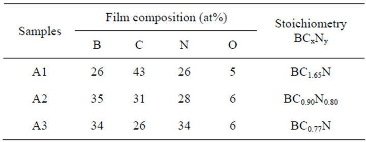
Table 2. Atomic composition of the as-deposited B-C-N hybrid films. The atomic composition was estimated from the intensity ratio of the XPS wide scan spectra.
 (a) (b) (c)
Figure 2. B1s, C1s, and N1s XP spectra of the samples shown in Figure 1 together with the single Gaussian curve (broken line) and the deconvoluted component peaks (dotted line). The corresponding substrate temperatures are also shown in the figure.
is ascribed to the sp2-B-N bonds in h-BN based ontheir reported binding energy which was found in the range of 190.0 - 191.0 eV [29-31].
However, it is not easy to distinguish the B-N bonds from the B-C-N hybrid because the B, C, and N atoms are bonded in the chemical environment similar to the BN3-like configurations. Moreover, h-BN and graphite are isoelectronic and lattice parameters of the h-BCN, h-BN and graphite are very similar [32]. Therefore, the component peak at 189.6 eV has been assigned to the sp2-B-C-N atomic hybrid configuration as we reported previously [15-18].
The FWHM for these samples (A1 = 3.2 ev, A2 = 3.1 ev, and A3 = 3.1 ev) were found to be almost comparable. It indicates that the predominant BCN atomic hybrids were formed on the substrate. As we discussed above, the B1s peak could be fitted by a symmetrical single Gaussian curve with broad FWHM, therefore, formation of the separated binary phases such as BCx and/or BN was not obvious.
Similar to the B1s XPS spectra, FWHM of the C1s spectra for all the samples was also significantly larger than that of graphite. The C1s spectra were fitted by deconvoluting into component peaks (Figures 2(b)). The dominating peak centered at 284.2 eV could be ascribed to the C=C bonds as in graphite [33]. The deconvoluted peak centered at 283.2 eV suggests formation of C-B bond, because the C1s peak energies for BC3.4 and B4C have been reported at 284.3 and 283.0 eV, respectively [30]. The component peak at the higher binding energy region centered at around 286.0 eV is due to C atom bonded to more electronegative N atom [34].
Figures 2(c) showed N1s XPS spectra and it has been observed that all the N1s spectra are found to be almost Gaussian like single symmetrical centered at around 398.4 eV. It implies that the chemical environment around the N atoms is mainly due to the formation of sp2-N-B bonds. Although the peak position for the samples A1 and A2 is shifted towards lower binding energy region by 0.4 eV. It has been reported that the N1s binding energy for sp2-N-B bonds is in the region of  [31,35]. Moreover, in some studies the peak at around 398.4 eV is also reported for sp2-C-N bonds [36,37]. Hence, this arise a significant ambiguity in the interpretation of N1s XP spectra. The N-B bonds are predominant in accordance with the fact suggested from the B1s (Figure 2(a)) spectra while the intensity of the N-C bonds obtained from the deconvolution of C1s spectra is insignificant.
By analyzing the B1s, C1s and N1s XP spectra, it has been suggested that the films are composed of different B-N, B-C and C-N bonds in forming the ternary B-C-N atomic hybrid configurations. The wider FWHM of the B1s peaks in comparison with that of the h-BN suggests the B atoms have various chemical environments other than the BN3 configuration similar to h-BN. The C1s and N1s peaks also imply that the C atoms are not only bonded to C to form the graphite-like configuration but also bonded to B and N in forming the sp2-B-C-N chemical environments. For further assessment of the local structure and orientation, we performed NEXAFS measurement. Since the NEXAFS is very sensitive for the element specific analysis.
3.3. NEXAFS Analyses
Polarization dependence of NEXAFS spectra can be simply described by the following equation [23]
 (1)
(1)
where Iif , O, and d are the peak intensity of the NEXAFS spectrum, orbital vector of the final state, angle between the electric field vector E and direction of the final state molecular orbital vector O, respectively. In the case of C K-edge NEXAFS for HOPG, the p* orbital is just perpendicular to the surface of HOPG, thus E has large projection to that orbital when the X-ray has a grazing incidence angle [38]. Based on this principle we, therefore, discussed the polarization dependence of NEXAFS spectra in order to clearly clarify the orientation of the present samples.
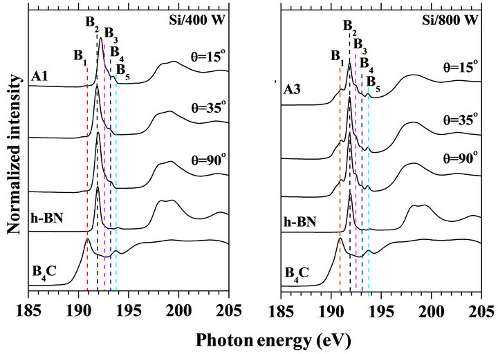
Figures 3(a) and (b) show B K-edge NEXAFS spectra at various incident angles of the X-ray for the samples synthesized at 400 and 800 W, respectively together with the spectra of the h-BN and B4C powders as the references. The vertical scales of the NEXAFS spectra for three incident angles were normalized by the intensities of the respective spectra at 230 eV where no polarization dependence existed. At the normal incidence (θ = 90˚) of X-ray, a broad peak (peak B2) as compared with the hBN has been predominantly observed at photon energy around 192.0 eV. The dominating feature of peak B2 was supposed to be the p* resonance of the sp2-B-C-N bonds suggesting dominant formation of hexagonal sp2-BCN compound with similar configuration like-BN3 in h-BN.
At the grazing incidence angle (θ = 15˚), the B2 peak height was decreased specially in the case of the sample synthesized at high substrate temperature. In addition, some fine structures such as B1 (190.7 eV), B3 (192.5 eV), and B4 (at 195.1 eV) were found to be clearer for the samples synthesized at 800˚C (Figure 3(b)). These indicate that formation of various chemical environments around B atoms besides the BN3-like configuration was evident. The fine structure B1 could be ascribed to the B atoms bonded to B in B4-C-like chemical environment because of the similar photon energy of B4C [39] and/or the sp2-B-C3-like chemical environment [40]. According to the core-level shift model, the fine structures B3 and B4 have been assigned to B-O2C and B-ON2, respectively, oxygen-saturated nitrogen vacancies around B chemical environment by Caretti et al. [40,41]. The interpretation is supportive, since all the samples containing oxygen impurities confirmed by XPS wide scan spectra. However, the fine structures could not be simply ascribed to the B atoms bonded to N and C atoms such as BN2C or BNC2 configuration, since the photon energy of B Kedge might decrease by substituting C for more electronegative N atoms around the B atoms. The steric configurations of these different atomic hybrids of BCN have not been identified clearly yet although the different BCN atomic hybrid configurations with different N vacancies might be formed [1]. The fine structure B5 centered at 193.7 eV is assigned to be the B-O bond which was estimated as the surface contamination for these present samples.
The decrease of B2 peak height (Figure 3(b)) suggests that the h-BCN layers have ordered structure and ori-
 (a) (b)
Figure 3. Normalized B K-edge NEXAFS spectra at various incident angles (q) of the X-ray: The samples were synthesized at 400, and 800 W at the substrate temperature of 700˚C and 800˚C, respectively. The B K-edge NEXAFS spectrum of the h-BN and B4C powders are shown in the bottom of the figure for comparison.
ented in the direction perpendicular to the Si substrate surface [42]. The orientated structure of the h-BCN films on the substrate may correspond to the sharp XRD peak at 2θ = 26.3˚ for the sample synthesized at 800˚C.
Figures 4(a) and (b) show polarization dependence of N K-edge NEXAFS spectra at various incident angles of X-ray for the samples prepared at 400 and 800 W, respectively together with the spectrum of the h-BN powder as the reference. The p* resonance peak of N K-edge is shifted by ~2.0 eV to the high photon energy region and does not significantly change with the grazing incidence angle. It hence means that the orientation of the sp2-BCN basal planes with h-BN-like configuration was perpendicular to the substrate. Moreover, the fine structures are not appearing in the N K-edge spectra and the spectra for these present samples are very similar to each other. This observation suggests that the atomic arrangement around N atoms is highly homogenous and very similar to each other in comparison with those around the B atoms. One can also be indicated that N K-edge spectra are not so sensitive in changing the chemical environment. However, it is difficult to distinguish the atomic arrangements around N atom because the peak energies correspond to the N-B and N-C bonds are very close to each other [43].
Theoretical calculations for energy separation of B1s®p* and B1s®s* resonances of graphite-like BC2N system have been carried out at 7.0 - 8.5 eV [3,44,45]. The energy separation (p* to s* state) for the present samples was found to be around 7.5 - 8.0 eV which was in good agreement with the reported energy. Furthermore, it has been reported that the hexagonal h-BCN structure will be dominant for N content over 20 at% [46]. The N content
 (a) (b)
Figure 4. Normalized N K-edge NEXAFS spectra at various incident angles (q) of the X-ray: The samples were synthesized at 400, and 800 W at the substrate temperature of 700˚C and 800˚C, respectively. The N K-edge NEXAFS spectrum of the h-BN and is shown in the bottom of the figure for comparison.
in the present samples was found to be around 26 to 34 at% (Table 2). Again, the hexagonal structure will be retained with a limiting C concentration of ~30 at% without breaking the h-BCN symmetry. For higher C concentration up to a ~65 at%, a dominant amorphization will be occurred [47]. The C content in the present samples was found to be around 26 to 43 at% (Table 2).
Based on these facts, therefore, it was confirmed that the h-BCN compound composed of a real sp2-BCN configuration and it was perpendicularly oriented on the Si substrate.
3.4. Raman Analyses
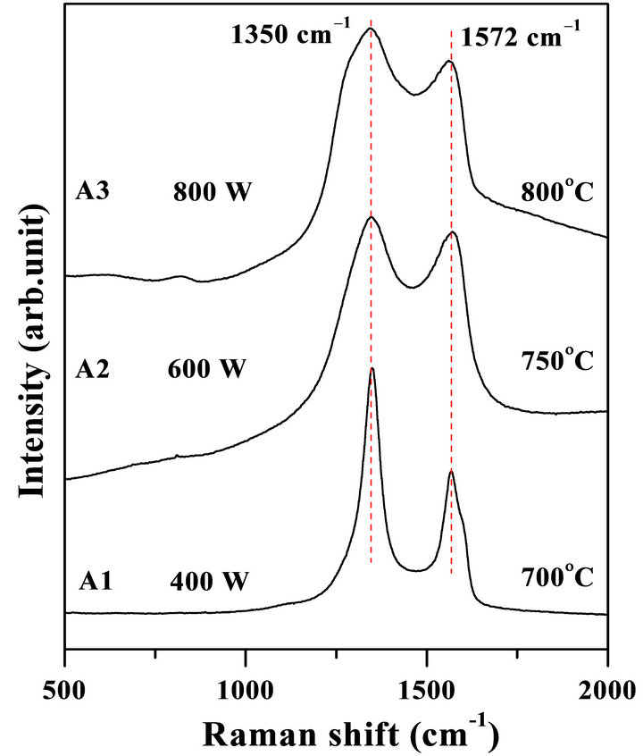
Raman spectroscopy has been applied in order to confirm the formation of crystalline hexagonal structure. Figure 5 shows Raman spectra for the samples shown in Figure 1. Two bands are observed at 1350 cm−1 and 1572 cm−1 (known as D and G band, respectively) in these spectra. The D and G peaks in the Raman spectra are usually assigned for the distorted and pure graphitic band. However, origin of the D peak has not been clearly clarified [48]. Although, Ferrari and Robertson have tried to interpret origin of the D and G peaks for disordered and amorphous carbon [49]. It has been observed that, both the D and G peaks are found to be RF power as well as temperature dependent. Since the  ratio has been considering the degree of disordered structure, therefore, the results suggest that RF power and substrate temperature might influence on the crystallinity of these samples [50]. Based on Raman analyses, it has been suggested that all the samples are supposed to be composed of graphite-like nano-crystalline h-BCN compound. The
ordered structure of the films has been improved with the substrate temperature at 800˚C.
3.5. Microstructure Analyses
Figure 6 shows high resolution FE-SEM surface micrographs for the samples prepared at different substrate temperatures. FE-SEM images revealed that a well-defined micrometer scale crystalline structures, around 10 µm thick, deposit on the substrate surface. Image for sample A3, prepared at 800˚C, average size of the nanocrystal is smaller than that of the other images.
4. Conclusion
We have studied the hexagonal nano-crystalline h-BCN compound synthesized by RF-PECVD using TDMAB as the single-source molecular precursor. The nano-crystalline hexagonal structure was confirmed by XRD and FESEM. The broad and almost symmetric XP spectra suggest that the films were composed of different B-N, B-C, and C-N bonds in forming the sp2-B-C-N atomic hybrid configuration. Evidence for the formation of binary compounds such as BN/graphite/CNx/BCx was not assumed since the XP spectra were not splitted nor shifted. NEX AFS measurements also confirmed the predominant formation of the h-BCN configuration together with some fine structures in the samples synthesized at 800˚C. The polarization dependence of the B K-edge and N K-edge NEXAFS spectra revealed that the h-BCN are oriented in the direction perpendicular to the Si substrate.
5. Acknowledgements
The authors are grateful to the staff of KEK-PF for their supports to run the experiment using synchrotron radiation and thanks to Dr. Y. Kitajima for his kind efforts in
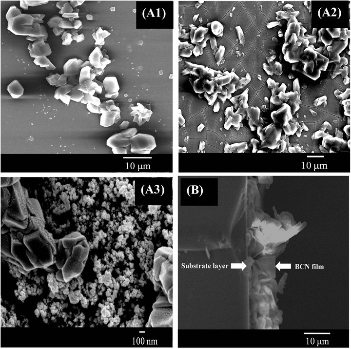
Figure 6. High-resolution FE-SEM surface micrograph of the samples (A1)-(A3). (B) is the cross-section image of FE-SEM presenting thickness of the typical sample (A3).
NEXAFS measurements. The XPS and the NEXAFS measurements were performed under the approval of the Photon Factory Program Advisory Committee (Proposal No. 2008G502). Special thanks to Dr. Unno Masashi, Saga University, for his kindest supports for measuring Raman spectra in his laboratory. This work was also supported by the Sasakawa Scientific Research Grant (Project No.20-331), Japan Science Society (JSS).
REFERENCES
- I. Jiménez, A. F. Jankowski, L. J. Terminello, D. G. J. Sutherland, J. A. Carlisle, G. L. Doll, W. M. Tong, D. K. Shuh and F. J. Himpsel, “Core-Level Photoabsorption Study of Defects and Metastable Bonding Configurations in Boron Nitride,” Physical Review B, Vol. 55, No. 18, 1997, pp. 12025-12037. doi:10.1103/PhysRevB.55.12025
- M. Wibbelt, H. Kohl and Ph. K. Redlich, “Multiple-Scattering Calculations of Electron-Energy-Loss Near-Edge Structures of Existing and Predicted Phases in the Ternary System B-C-N,” Physical Review B, Vol. 59, No. 18, 1999, pp. 11739-11745. doi:10.1103/PhysRevB.59.11739
- A. Y. Liu, R. M. Wentzcovitch and M. L. Cohen, “Atomic Arrangement and Electronic Structure of BC2N,” Physical Review B, Vol. 39, No. 3, 1989, pp. 1760-1765. doi:10.1103/PhysRevB.39.1760
- W. R. L. Lambrecht and B. Segall, “Anomalous BandGap Behavior and Phase Stability of c-BN-Diamond Alloys,” Physical Review B, Vol. 47, No. 15, 1993, pp. 9289- 9296. doi:10.1103/PhysRevB.47.9289
- J. Yu, X. D. Bai, J. Ahn, S. F. Yoon and E. G. Wang, “Highly Oriented Rich Boron B-C-N Nanotubes by BiasAssisted Hot Filament Chemical Vapor Deposition,” Chemical Physics Letter, Vol. 323, No. 5-6, 2000, pp. 529- 533. doi:10.1016/S0009-2614(00)00546-7
- M. Kawaguchi, “B/C/N Materials Based on the Graphite Network,” Advanced Materials, Vol. 9, No. 8, 1997, pp. 615-625. doi:10.1002/adma.19970090805
- M. C. Polo, E. Martinez, J. Esteve and J. L. Andujar, “Preparation of B-C-N Thin Films by r.f. Plasma Assisted CVD,” Diamond and Related Materials, Vol. 7, 1998, pp. 376-379. doi:10.1016/S0925-9635(97)00167-2
- L. Liu, Y. Wang, K. Feng, Y. Li, W. Li, C. Zhao and Y. Zhao, “Preparation of Boron Carbon Nitride Thin Films by Radio Frequency Magnetron Sputtering,” Applied Surface Science, Vol. 252, No. 2-5, 2006, pp. 4185-4189. doi:10.1016/j.apsusc.2005.06.025
- A. Essafti, E. Ech-chamikh and J. L. G. Fierro, “Structural and Chemical Analysis of Amorphous B-N-C Thin Films Deposited by RF Sputtering,” Diamond and Related Materials, Vol. 14, No. 10, 2005, pp. 1663-1668. doi:10.1016/j.diamond.2005.06.005
- C. Popov, K. Saito, B. Ivanov, Y. Koga, S. Fujiwara and V. Shanov, “Chemical Vapour Deposition of BC2N Films and Their Laser-Induced Etching with SF6,” Thin Solid Films, Vol. 312, 1998, pp. 99-105. doi:10.1016/S0040-6090(97)00694-9
- M. Mieno and T. Satoh, “Study of BCN Compounds Prepared by the Chemical Vapor Deposition with Dimethylamineborane,” Journal of Materials Science, Vol. 36, No. 16, 2001, pp. 3925-3931. doi:10.1023/A:1017966004367
- T. Yuki, S. Umeda and T. Sugino, “Electrical and Optical Characteristics of Boron Carbon Nitride Films Synthesized by Plasma-Assisted Chemical Vapor Deposition,” Diamond and Related Materials, Vol. 13, No. 4-8, 2004, pp. 1130-1134. doi:10.1016/j.diamond.2004.01.005
- S. Ulrich, A. Kratzsch, H. Leiste, M. Stüber, P. Schloß- macher, H. Holleck, J. Binder, D. Schild, S. Westermeyer, P. Becker and H. Oechsner, “Variation of Carbon Concentration, Ion Energy, and Ion Current Density of Magnetron-Sputtered Boron Carbonitride Films,” Surface and Coating Technology, Vol. 116-119, 1999, pp. 742-750. doi:10.1016/S0257-8972(99)00353-9
- V. P. Filonenko, V. N. Khabashesku, V. A. Davydov, I. P. Zibrov and V. N. Agafonov, “Synthesis of a New Cubic Phase in the B-C-N System,” Inorganic Materials, Vol. 44, No. 4, 2008, pp. 395-400. doi:10.1134/S0020168508040122
- M. A. Mannan, M. Nagano, N. Hirao and Y. Baba, “Hexagonal BCN Films Prepared by RF Plasma-Enhanced CVD,” Chemistry Letter, Vol. 37, No. 1, 2008, pp. 96-97. doi:10.1246/cl.2008.96
- M. A. Mannan, M. Nagano, T. Kida, N. Hirao and Y. Baba, “Characterization of BCN Films Synthesized by Radiofrequency Plasma Enhanced Chemical Vapor Deposition,” Journal of Physics and Chemistry of Solids, Vol. 70, No. 1, 2009, pp. 20-25. doi:10.1016/j.jpcs.2008.08.013
- M. A. Mannan, H. Noguchi, T. Kida, M. Nagano, N. Hirao and Y. Baba, “Chemical Bonding States and Local Structures of the Oriented Hexagonal BCN Films Synthesized by Microwave Plasma CVD,” Materials Science and Semiconductor Processesing, Vol. 11, No. 3, 2008, pp. 100-105. doi:10.1016/j.mssp.2009.04.003
- M. A. Mannan, H. Noguchi, T. Kida, M. Nagano, N. Hirao and Y. Baba, “Growth and Characterization of Stoichiometric BCN Films on Highly Oriented Pyrolytic Graphite by Radiofrequency Plasma Enhanced Chemical Vapor Deposition,” Thin Solid Films, Vol. 518, No. 15, 2010, pp. 4163-4169. doi:10.1016/j.tsf.2009.11.086
- M. A. Mannan, Y. Baba, T. Kida, M. Nagano, I. Shimoyama, N. Hirao and H. Noguchi, “Orientation of B-C-N Hybrid Films Deposited on Ni (111) and Polycrystalline Ti Substrates Explored by X-Ray Absorption Spectroscopy,” Thin Solid Films, Vol. 519, No. 6, 2011, pp. 1780- 1786. doi:10.1016/j.tsf.2010.09.052
- J. H. Scofield, “Theoretical Photoionization Cross Section from 1 to 1500 keV,” Lawrence Livermore Laboratory, Livermore, 1973.
- R. Franke, St. Bender, H. Jüngermann, M. Kroschel and M. Jansen, “The Determination of Structural Units in Amorphous Si-B-N-C Ceramics by means of Si, B, N and C K-XANES Spectroscopy,” Journal of Electron Spectroscopy and Related Phenomenon, Vol. 101-103, 1999, pp. 641-645. doi:10.1016/S0368-2048(98)00328-4
- D. Li, G. M. Bancroft and M. E. Fleet, “B K-edge XANES of Crystalline and Amorphous Inorganic Materials,” Journal of Electron Spectroscopy and Related Phenomenon, Vol. 79, 1996, pp. 71-73. doi:10.1016/0368-2048(96)02805-8
- J. Stöhr, “XEXAFS Spectroscopy, Springer Series in Surface Sciences,” Vol. 25, Springer, Berlin, 1996.
- R. Torres, I. Caretti, R. Gago, Z. Martín and I. Jiménez, “Bonding Structure of BCN Nanopowders Prepared by Ball Milling,” Diamond and Related Materials, Vol. 16, No. 4-7, 2007, pp. 1450-1454. doi:10.1016/j.diamond.2007.01.009
- Z. F. Zhou, I. Bello, M. K. Lei, K. Y. Li, C. S. Lee and S. T. Lee, “Synthesis and Characterization of Boron Carbon Nitride Films by Radio Frequency Magnetron Sputtering,” Surface and Coating Technology, Vol. 128-129, 2000, pp. 334-340. doi:10.1016/S0257-8972(00)00600-9
- A. Perrone, A. P. Caricato, A. Luches, M. Dinescu, C. Ghica, V. Sandu and A. Andrei, “Boron Carbonitride Films Deposited by Pulsed Laser Ablation,” Applied Surface Science, Vol. 133, No. 4, 1998, pp. 239-242. doi:10.1016/S0169-4332(98)00207-4
- C. Morant, P. Prieto, J. Bareño, J. M. San and E. Elizalde, “Hard BCxNy Thin Films Grown by Dual Ion Beam Sputtering,” Thin Solid Films, Vol. 515, No. 1, 2006, pp. 207- 211. doi:10.1016/j.tsf.2005.12.063
- M. O. Watanabe, S. Itoh, K. Mizushima and T. Sasaki, “Bonding Characterization of BC2N Thin Films,” Applied Physics Letter, Vol. 68, 1996, pp. 2962-2964. doi:10.1063/1.116369
- W. J. Pan, J. Sun , H. Ling, N. Xu, Z. F. Ying and J. D. Wu, “Preparation of Thin Films of Carbon-Based Compounds,” Applied Surface Science, Vol. 218, No. 1-4, 2003, pp. 298-305. doi:10.1016/S0169-4332(03)00622-6
- M. O. Watanabe, T. Sasaki, S. Itoh and K. Mizushima, “Structural and Electrical Characterization of BC2N Thin Films,” Thin Solid Films, Vol. 281-282, 1996, pp. 334- 336. doi:10.1016/0040-6090(96)08656-7
- M. N. Uddin, I. Shimoyama, Y. Baba, T. Sekiguchi and M. Nagano, “X-Ray Photoelectron Spectroscopic Observation on B-C-N Hybrids Synthesized by Ion Beam Deposition of Borazine,” Journal of Vacuum Science and Technology A, Vol. 23, No. 3, 2005, pp. 497-502. doi:10.1116/1.1894667
- Yu. G. Andreev and T. Lundstrom, “High-Temperature Synthesis and Investigation of Hexagonal Boron Carbonitride,” Journal of Alloys and Compounds, Vol. 210, No. 1-2, 1994, pp. 311-317. doi:10.1016/0925-8388(94)90155-4
- M. Dinescu, A. Perrone, A. P. Caricato, L. Mirenghi, C. Gerardi, C. Ghica and L. Frunza, “Boron Carbon Nitride Films Deposited by Sequential Pulses Laser Deposition”, Applied Surface Science, Vol. 127-129, 1998, pp. 692- 696. doi:10.1016/S0169-4332(97)00727-7
- V. Linss, S. E. Rodil, P. Reinke, M. G. Garnier, P. Oelhafen, U. Kreissig and F. Richte, “Bonding Characteristics of DC Magnetron Sputtered B-C-N Thin Films Investigated by Fourier-Transformed Infrared Spectroscopy and X-Ray Photoelectron Spectroscopy,” Thin Solid Films, Vol. 467, No. 1-2, 2004, pp. 76-87. doi:10.1016/j.tsf.2004.03.009
- I. Shimoyama, G. Wu, T. Sekiguchi and Y. Baba, “Study of Electronic Structure of Graphite-Like Carbon Nitride,” Journal of Electron Spectroscopy and Related Phenomenon, Vol. 114-116, 2001, pp. 841-848. doi:10.1016/S0368-2048(00)00306-6
- X. Li, J. Zhang, L. Shen, Y. Ma, W. Lei, Q. Cui and G. Zou, “Preparation and Characterization of Graphitic Carbon Nitride through Pyrolysis of Melamine,” Applied Physics A, Vol. 94, 2009, pp. 387-392. doi:10.1007/s00339-008-4816-4
- P. Hammer and F. Alvarez, “Influence of Chemical Sputtering on the Composition and Bonding Structure of Carbon Nitride Films,” Thin Solid Films, Vol. 398-399, 2001, pp. 116-123. doi:10.1016/S0040-6090(01)01456-0
- R. A. Rosenberg, P. J. Love and V. Rehn, “PolarizationDependent C(K) Near-Edge X-Ray Absorption Fine Structure of Graphite,” Physical Review B, Vol. 33, 1986, pp. 4034-4037. doi:10.1103/PhysRevB.33.4034
- R. Gago, I. Jiménez, I. García and J. M. Albella, “Growth and Characterisation of Boron-Carbon-Nitrogen Coatings Obtained by Ion Beam Assisted Evaporation,” Vacuum, Vol. 64, No. 3-4, 2002, pp. 199-204. doi:10.1016/S0042-207X(01)00314-1
- I. Caretti and I. Jiménez, “Point Defects in Hexagonal BN, BC3 and BCxN Compounds Studied by X-Ray Absorption Near-Edge Structure,” Journal of Applied Physics, Vol. 110, No. 2, 2011, Article ID: 023511. doi:10.1063/1.3602996
- I. Caretti and I. Jiménez, “Composition and Bonding Structure of Boron Nitride B1−xNx Thin Films Grown by Ion-Beam Assisted Evaporation,” Chemical Physics Letters, Vol. 511, No. 4-6, 2011, pp. 235-240. doi:10.1016/j.cplett.2011.06.001
- R. Gago, I. Jiménez, T. Sajavaara and J. M. Albella, “XRay Absorption Studies of Cubic Boron-Carbon-Nitrogen Films Grown by Ion Beam Assisted Evaporation,” Diamond and Related Materials, Vol. 10, No. 3-7, 2001, pp. 1165-1169. doi:10.1016/S0925-9635(00)00414-3
- S. C. Ray, H. M. Tsai, J. W. Chiou, J. C. Jan, K. Kumar, W. F. Pong, F. Z. Chien, M. H. Tsai, S. Chattopadhyay, L. C. Chen, S. C. Chien, M. T. Lee, S. T. Lin and K. H. Chen, “X-Ray Absorption Studies of Boron-Carbon-Nitrogen (BxCyNz) Ternary Alloys,” Diamond and Related Materials, Vol. 13, No. 4-8, 2004, pp. 1553-1557. doi:10.1016/j.diamond.2003.11.052
- J. Kouvetakis, T. Sasaki, C. Shen, R. Hagiwara, M. Lerner, K. M. Krishnan and N. Bartlett, “Novel Aspects of Graphite Intercalation by Fluorine and Fluorides and New B/C, C/N and B/C/N Materials Based on the Graphite Network,” Synthetic Metals, Vol. 34, No. 1-3, 1989, pp. 1-7. doi:10.1016/0379-6779(89)90355-X
- Z. Weng-Sieh, K. Cherrey, N. G. Chopra, Y. Miyamoto, A. Rubio, M. L. Cohen, S. G. Louie, A. Zettl and R. Gronsky, “Synthesis of BxCyNz Nanotubules,” Physical Review B, Vol. 51, No. 16, 1995, pp. 11229-11232. doi:10.1103/PhysRevB.51.11229
- R. Gago, I. Jiménez and J. M. Albella, “Identification of Ternary Boron-Carbon-Nitrogen Hexagonal Phases by XRay Absorption Spectroscopy,” Applied Physics Letter, Vol. 78, No. 22, 2001, pp. 3430-3432. doi:10.1063/1.1376428
- I. Caretti, R. Torres, R. Gago, A. R. Landa-Canovas and I. Jiménez, “Effect of Carbon Incorporation on the Microstructure of BCxN (x = 0.25, 1, and 4) Ternary Solid Solutions Studied by Transmission Electron Microscopy,” Chemical Materials, Vol. 22, No. 6, 2010, pp. 1949-1951. doi:10.1021/cm9038472
- T. Hagio, M. Nakamizo and K. Kobayashi, “Studies on X-Ray Diffraction and Raman Spectra of B-Doped Natural Graphite,” Carbon, Vol. 27, No. 2, 1989, pp. 259-263. doi:10.1016/0008-6223(89)90132-2
- A. C. Ferrari and J. Robertson, “Interpretation of Raman Spectra of Disordered and Amorphous Carbon,” Physical Review B, Vol. 61, No. 20, 2000, pp. 14095-14107. doi:10.1103/PhysRevB.61.14095
- S. Ulrich, T. Theel, J. Schwan and H. Ehrhardt, “Magnetron-Sputtered Superhard Materials,” Surface and Coating Technology, Vol. 97, No. 1-3, 1997, pp. 45-69. doi:10.1016/S0257-8972(97)00159
NOTES
*Corresponding author.


