Circuits and Systems
Vol.5 No.4(2014), Article ID:44309,9 pages DOI:10.4236/cs.2014.54011
MMCC Based Electronically Tunable Allpass Filters Using Grounded Synthetic Inductor
Rabindranath Nandi1*, Palaniandavar Venkateswaran1, Mousiki Kar2
1Department of Electronics & Telecommunication Engineering, Jadavpur University, Kolkata, India
2Department of Electronics & Communication Engineering, Heritage Institute of Technology, Kolkata, India
Email: *robnon@ieee.org, pvwn@ieee.org, mousikikar@gmail.com
Copyright © 2014 by authors and Scientific Research Publishing Inc.
This work is licensed under the Creative Commons Attribution International License (CC BY).
http://creativecommons.org/licenses/by/4.0/


Received 28 January 2014; revised 28 February 2014; accepted 7 March 2014
ABSTRACT
New circuit implementations of electronically tunable first and second order allpass filter (AP) structures using a Multiplication Mode Current Conveyor (MMCC) building block are presented. The control voltage (V) of the MMCC tunes the desired phase (θ) while the time constant (τ) is adjustable by a Differential Voltage Current Conveyor Transconductance Amplifier (DVCCTA)-based synthetic lossless grounded inductor (L). The circuits are analyzed taking into account the device imperfections which show low active sensitivity features of the designs. The effects of port transfer error (ε) and that of the parasitic capacitances of the active devices had been meticulously examined which indicated that certain deviations in nominal design equations occur; these however, could be minimized with appropriate choice of the circuit passive components. Readily available AD-844 type Current Feedback Amplifier (CFA) elements are utilized for the topology implementation. Satisfactory test results on electronic θ-tunability, upto about 300 KHz, had been verified by PSPICE simulation and with hardware experimentation.
Keywords:Allpass Filter; MMCC; DVCCTA; CFA; Synthetic Inductor; Electronic Phase Shifter

1. Introduction
AP filters are special purpose function circuits which provide variable phase response [1] -[13] in a prescribed frequency band keeping the transmission gain constant. These filters are widely used in communication systems as phase/delay equalizers, phase injector for stability improvement [14] , in phase lock loop (PLL) and in voltage controlled oscillator (VCO) design. The functional versatility improves significantly if the phase could be tuned electronically.
The literature indicates that many such variable phase AP filter design schemes had been proposed using various types of active building blocks, e.g., voltage operational amplifier [1] -[3] , current conveyor (CC) [4] -[6] , DVCCTA [7] , fully differential current conveyor (FDCC) [8] , differential difference amplifier (DDA) [9] , current inverting transconductance amplifier (CITA) [10] , operational transconductance amplifier (OTA) [11] , voltage differencing differential input buffered amplifier (VD-DIBA) [12] , differential voltage current conveyor (DVCC) [12] . While most of these designs are passive tuned, recent attention appears to be on electronic phase tunability aspect [15] -[17] . It is seen that for electronic tuning, usually the bias current of a transconductance (gm) block is utilized. This involves elaborate current processing circuitry and additional quiescent power requirement along side.
Here we propose that the recently introduced MMCC building block [18] is quite amenable to this purpose if its control voltage terminal is utilized. The use of MMCC device for such AP filters had not yet been reported. The control voltage here may be directly fed ensuring circuit simplicity and suitability for integration. In our design, a four-quadrant multiplier [19] [20] device (ICL-8013 or AD-534) had been coupled at the front end of the MMCC device implementation while its back end is fabricated with AD-844 CFA element [20] -[23] .
The phase selective component is a DVCCTA based synthetic lossless grounded inductor (L) as proposed recently by our research group [24] ; it is connected to the current source x-terminal of the MMCC. The first order transfer (H1) is derived by connecting only the synthetic-L while second order function (H2) is obtained by forming a series LC resonator with a capacitor (C).
The effects of the device imperfections, viz., port tracking error (ε) and parasitic shunt-rC components of both the devices have been carefully analyzed. The findings indicate that through appropriate design and with suitable choice of the active-L component, the deviations could be made insignificant leading to low active-sensitivity realization. All the analytical derivations are supported by experimental verification with PSPICE simulation [25] and by hardware test using the multiplier-CFA composite device implementation. There are several advantageous features of the CFA-AD-844 IC-chip with respect to low noise at extremely small tracking error  and, superior bandwidth and slew rate capabilities [20] -[23] .
2. Circuit Analysis and Design
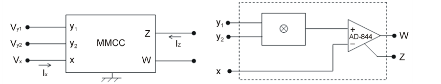
The building blocks and their device implementation schemes are shown in Figure 1. The MMCC block in Figure 1(a), is configured with ICL-8013 (and also AD-534 as a variant) and AD-844 CFA. The nodal relations are  and
and . The control voltage (V) is applied at y2 terminal where k (= 0.1/volt) is the multiplication constant and input signal Vi is applied at y1 terminal. We verified that polarity of MMCC could be made simply inverting or noninverting by altering the sign of V. The CFA nodal relations are
  and
and  while
while . The port transfer coefficients may be postulated as
  where
where . Hence in Figure 1(b) we get
  and
and  which is an additional voltage source output node, not usually depicted in conventional current conveyor; with ± V one gets a ±MMCC block.
The nodal relations of the DVCCTA block as in Figure 1(c) are  and
and ; here also we may define the tracking ratios in terms of finite-ε error. The DVCCTA device implementation using AD-844 CFA element is shown in Figure 1(d).
The electronically tunable allpass filter (ETAF) topology is shown in Figure 2 while the two synthetic-L simulators are shown in Figure 3. The input admittance (Yi) of these simulators would be connected as the admittance Y3 in Figure 2. The various device parasitics are shown as the shunt-rC arms; typical values of these components [25] [26] are 2 MΩ < rp,z < 6 MΩ and 3 pF < Cp,z < 7 pF. Analysis assuming ideal devices in Figure 2 yields a voltage transfer  as
as
 (1)
(1)
where G1,2 are conductances; for proposed design we take  and Y3 would be the synthetic admittance of Figures 3(a) and (b) for the first order AP function. Next we propose two second order ETAF designs by considering Y3 as the series LC resonator of which the inductance would be utilized from the L-simulators of Figures 3(a) and (b) along with a passive capacitor.
 (a)
(a) (b)
(b)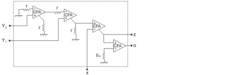 (c)
(c)
Figure 1. The active building blocks (a) MMCC device (b) MMCC implementation with commercially available IC-chips (c) DVCCTA device (d) DVCCTA device implementation with CFAs.
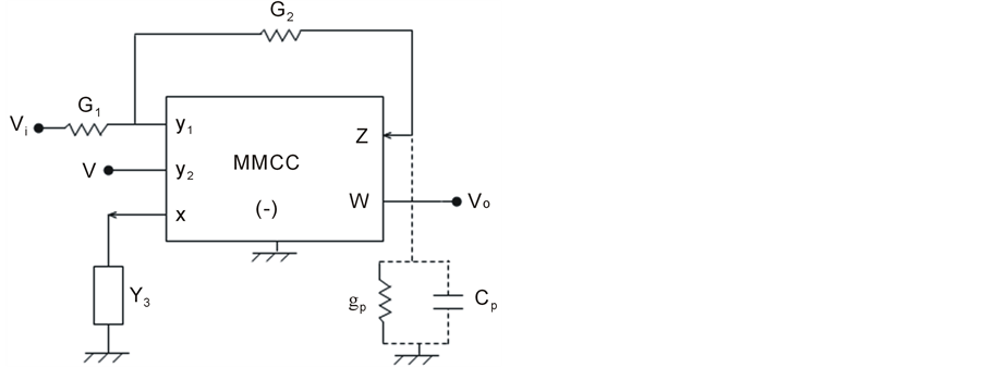
Figure 2. MMCC based AP filter structure.
3. First Order ETAF
We now present the first order ETAF realization in Figure 2 wherein the grounded admittance Y3 is being implemented by the input admittance Yi of Figures 3(a) and (b). The analysis is first carried out assuming ideal MMCC and DVCCTA building blocks, i.e. parasitics are negligible  and port errors are insignificant
 .
.
The first order AP function (H1) is derived assuming G1,2 = 1/R, as
 (2)
(2)
where . For both the topologies of the inductor simulators we have
  and
and  if
if .The select frequency is
  and the phase is
 . Thus the select frequency and the phase response are electronically tunable by the control voltage (V) in a range
 . Here no additional current processing circuitry is needed for tuning by gm.
 (a)
(a)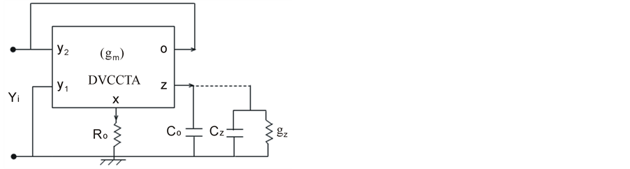 (b)
(b)
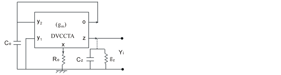
Figure 3. DVCCTA based L-simulators.
4. Second Order ETAF
The synthetic-L is seen to be lossless in Figure 3 under ideal conditions. For realizing the second order MMCC based ETAFs, we form a series-LC resonator using a passive capacitor with the L so that the series combination yields . Using this in Equation (1) and writing
  we get the second order (H2) AP functions while both topologies of Figure 3 are connected to node-x of Figure 1. Therefore H2 is
 (3)
(3)
where  and
and  is quality factor; simplified design equations are obtained if
  so that
  and
and . Phase variation is given by
 (4)
(4)
Thus θ is tunable by V while phase slope in the frequency response is adjusted by q. These results are summarized in Table 1.
5. Effects of Device Imperfections
The proposed AP circuit topologies have been thoroughly re-examined keeping in view the imperfections of the two types of devices used. These nonidealities are owing to finite port transfer ratio errors  and due to presence of the parasitic components appearing in the form of shunt-rp,zCp,z arms.
First we present the effect finite port error of the MMCC (α,β,δ)M and the DVCCTA (α,β,δ)D. Analysis shows that transfer function in Equation (1) modifies to
 . (5)
. (5)
Similarly L-values are altered:
 (6)
(6)
Combining Equations (5) with (6) and replacing Y3 by Yi, we observe that albeit the inductance value is slightly altered , it remains lossless in both structures of Figure 3 which implies that filter time constant is also altered
 . However, the nonminimum phase property of the filter function remains unaffected while θ will be tunable by V as per prescribed design.
Next we consider the effects of the finite parasitic components at the z-node of MMCC block (Cp, gp) and the DVCCTA block (Cz, gz).
The transfer now modifies to
 (7)
(7)
where .
.
Re-Analysis indicates that admittance in Figure 3(a) is
 (8)
(8)

Table 1. First and second order ETAF design with ideal devices.
which is the shunt combination of L with the parasitic components. The simulated impedance in Figure 3(b) is
 (9)
(9)
where  and
and .
.
Further detailed analysis had been carried out for examining the effects of these parasitics on the proposed first and second order ETAFs. These derivations are tabulated in a comprehensive manner in Table 2.
The findings on the phase calculations are listed in Table 3. One may observe that the parasitic capacitors affect the expected phase variation (θ) at higher frequency ranges by introducing a second order term being dominated by ωz; hence the higher side of the usable frequency will be limited by fz ≈ 3 MHz for Figure 3(a) and by fp ≈ 2.1 MHz for Figure 3(b) assuming a set of typical values of L = 1 mH, R = 1 KΩ, Cp ≈ Cz ≈ 3 pF and V ≈ 10 V.d.c. (max.)

For second order AP function design, the parasitic capacitors introduce a 3rd-order term in the transfer function that is being dominated by ωe and ωi; by the same set of values we get fe ≈ 960 KHz and fi ≈ 888 KHz which are the values of maximum upper operating frequency for the second order ETAF. It may be inferred that with appropriate choice of the nominal circuit components such that  and
and , the proposed filters would perform as per nominal design. This aspect had been meticulously verified with experimental work based by PSPICE simulation and with hardware circuit tests; the measured response is shown Figure 4.
Table 2. Effect of device parasitic on filter function.
Table 3. Phase calculation under non-ideal condition.
 (a)
(a)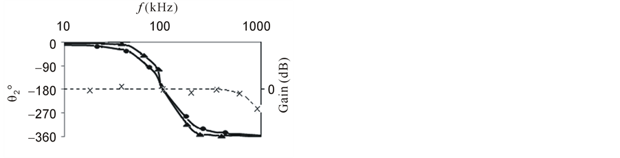 (b)
(b)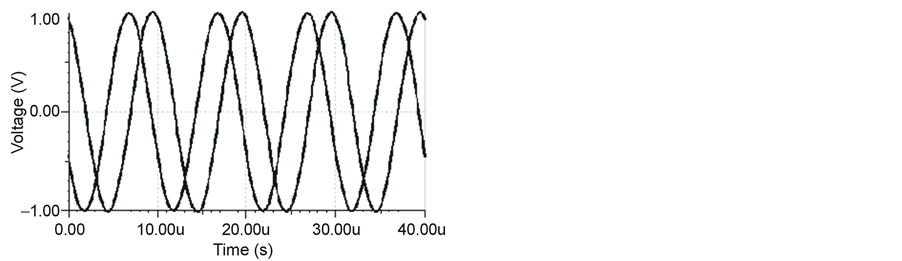 (c)
(c)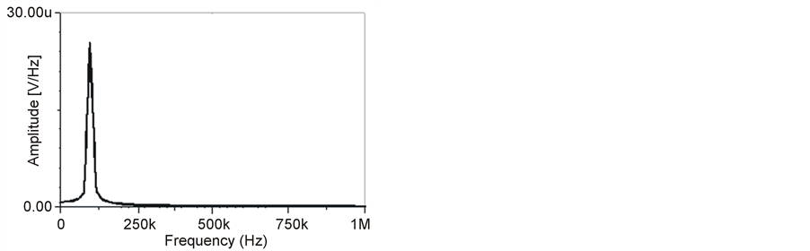 (d)
(d)
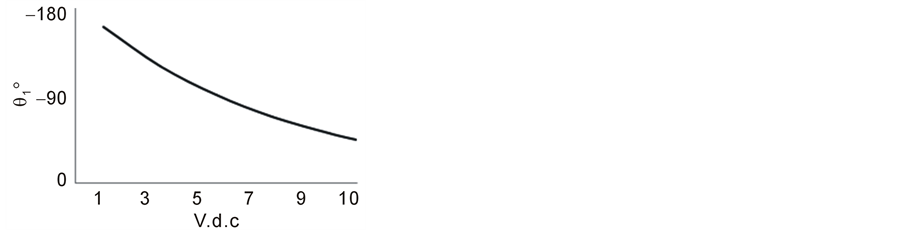
Figure 4. Experimental results on ETAFs (a) 1st order tested at 200 KHz with La = 0.4 mH, R = Ro = Rm = 1 KΩ, Co = 0.4 nF: θ1-Variation wth V (b) 2nd order θ2-response for q = 2,V = 5 ( ) and q = 5,V = 2 ( ) with Lb = 2.5 mH, C = Co = 1 nF, R = 1.6 KΩ; dotted line: magnitude reponse (c) Quadrature wave response of first order AP filter at 100 KHz (d) Spectrum of 90˚ phase shifted output signal.
6. Experimental Results
The proposed MMCC based ETAFs had been designed using the device implementation of Figure 1. The aspect of electronic tuning of the variable phase (θ) is achieved by simple adjustment of control voltage (1 V.d.c ≤ V ≤ 10 V.d.c) of the MMCC block. This tuning procedure had been found to be simpler with respect that used in some previous work [15] [17] where additional current control circuitry would be needed for gm-variation.
The phase selective elements are chosen here are DVCCTA-based synthetic lossless-L for first order AP function, and subsequently a second order AP function using a resonating capacitor in series with the synthetic-L. These component sets are connected at the x-node of the MMCC block. The MMCC device implementation in hardware had been obtained using the AD-844 CFA chip along with a multiplier ICL-8013 (or AD-534) chip. The phase response was measured using both PSPICE [25] simulation and by hardware test; we measured the parasitic capacitor values to be Cp ≈ 4.5 pF and Cz ≈ 6 pF at Vcc = ± 15 V.d.c. Satisfactory θ-tuning is obtained upto about 300 KHz by varying V for both first and second order ETAFs while transmission gain was observed at unity in this band.
The test results are shown in Figure 4 where La,b indicates the simulation of Figures 3(a) and (b). We chose the nominal components such that R  rp,z and C
  Cp,z so as to minimize the effects of the parasitic.
7. Conclusions
The proposed ETAF can be controlled through external DC voltage V. In this paper we present two new circuit realization schemes of ETAFs using the relatively new MMCC building block to which DVCCTA-based synthetic inductive input admittance [24] is conveniently connected; for the first order function we use only the synthetic-L while for the second order, a capacitor constituting to a series resonator is used. Both the building blocks are implemented with readily available multiplier and CFA IC-chips. Compared to other such schemes [15] [17] , here no additional current control circuitry is needed since electronic tuning is achieved by simply applying V to the MMCC control-node. This is an advantage in view of less hardware complexity and avoiding additional quiescent power dissipation leading to easy integrability.
The effects of device imperfections have been thoroughly analyzed. It is seen that port errors (ε) cause insignificant deviations on phase since active-Sτ sensitivity is quite low as  where
where . However, the parasitics introduce some deviations on θ-characteristics and reveal certain limits on the maximum usable frequency. With appropriate choice of the nominal circuit components, these deviations could be minimized.
The proposed circuit topology is based on the new MMCC device which is identified as a versatile CCCS building block with inherent voltage control functionality [18] offering the designer the distinct advantage of utilizing this attribute by simply connecting a voltage signal at one of its input nodes. Other such phase shifters use transconductance (gm) as a control parameter which subsequently is derived by a bias current that involves a nonlinear equation [7] ; hence limited operating range at the cost of complicated current processing circuitry leading to increased hardware density. Also here we utilized a DVCCTA based high-quality synthetic-L realized by only one grounded-RC section, i.e., the minimal passive count; this L is then connected to the MMCC block that needs also the minimal component count, i.e., only one resistor pair for the realizability. The same topology yields both first and second order functions as per design choice. Our study indicates that all electronic active building blocks devised hitherto contain parasitics [21] -[24] which influence the performance of the function circuit based on these. In the proposed work we had analyzed the parasitic effects extensively and obtained a congregated design based on the judicious choice of circuit components that insures sufficiently accurate voltage tuned phase variation at low sensitivity within the prescribed band as substantiated by the experimental results shown.
The practical performance of these ETAFs had been verified by hardware circuit fabrication and also with PSPICE simulation. Expected range of tunability of θ by V is obtained in a frequency band of upto 300 KHz. Some test results are presented showing the phase variation for two quality factor values (q = 2 and q = 5) of the second order ETAF. We are now studying on the design of linear voltage controlled quadrangle oscillator (VCQO) using these ETAFs as further work.
Acknowledgements
The authors wish to thank Ms. Sagarika Das, our research colleague, for carrying out some experimentation work.
References
- Ponsonby, J.E. (1966) Active Allpass Filter Using a Differential Operational Amplifier. Electronics Letters, 2, 134-135. http://dx.doi.org/10.1049/el:19660107
- Genin, R. (1968) Realisation of an Allpass Transfer Function Using Operational Amplifier. Proceedings of the IEEE, 56, 1746-1747. http://dx.doi.org/10.1109/PROC.1968.6731
- Nandi, R. (1977) New Allpass Phase Shifters. International Journal of Electronics, 42, 97-99. http://dx.doi.org/10.1080/00207217708900617
- Soliman, A.M. (1973) Inductorless Realization of Allpass Transfer Function Using the Current Conveyor. IEEE Transactions on Circuits and Systems I, 20, 80-81.
- Nandi, R. (1992) Novel Current Mode Allpass Phase Shifters Using a Current Conveyor. IEEE Transactions on Instrumentation and Measurement, 41, 553-555. http://dx.doi.org/10.1109/19.155925
- Higashimura, M. and Fukui, Y. (1990) Realization of Current Mode Allpass Networks Using a Current Conveyor. IEEE Transactions on Circuits and Systems I, 37, 6660-6661. http://dx.doi.org/10.1109/31.55015
- Pandey, N., Pandey, R. and Paul, S.K. (2012) A First Order Allpass Filter and its Application in a Quadrature Oscillator. Journal of the Electron Devices Society, 12, 772-777.
- Mohan, J., Maheshwari, S. and Chauhan, D.S. (2010) Voltage Mode Cascadable Allpass Sections using Single Active Element and Grounded Passive Components. Journal of Circuits and Systems—Scientific Research Publishing, 1, 5-11.
- Toker, A. and Ozoguz, S. (2004) Novel Allpass Filter Using Differential Difference Amplifier. AEU—International Journal of Electronics and Communications, 58, 153-155. http://dx.doi.org/10.1078/1434-8411-54100221
- Biolek, D. and Biolkova, V. (2009) Allpass Filter Employing One Grounded Capacitor and One active Element. Electronics Letters, 45, 807-808. http://dx.doi.org/10.1049/el.2009.0575
- Psychaslinos, C. and Pal, K. (2010) A Novel Allpass Current Mode Filter Realized Using a Minimum Number of Single-Output OTAs. Journal of Frequenz, 64,123-129.
- Biolek, D. and Biolkova, V. (2010) First Order Voltage Mode Allpass Filter Employing One Active Element and One Grounded Capacitor. Analog Integrated Circuits and Signal Processing, 65, 123-129.
- Ibrahim, A., Minaei, S. and Yuce, E. (2012) Allpass Sections with Rich Cascadability and IC Realization Suitability. International Journal of Circuit Theory Applications, 40, 461-472.
- Wangenheim, L.V. (2012) Phase Margin Determination in a Closed Loop Configuration. Journal of Circuit System and Signal Processing, 31, 1917-1926. http://dx.doi.org/10.1007/s00034-012-9437-7
- Herencsar, N., Minaei, S., Koton, S., Yuce, E. and Vrba, K. (2013) New Resistorless and Electronically Tunable realization of Dual-Output VM Allpass Filter Using VDIBA. Journal of Analog Integrated Circuits and Signal Processing, 74, 141-154. http://dx.doi.org/10.1007/s10470-012-9936-2
- Nandi, R., Kar, M. and Das, S. (2009) Electronically Tunable Dual-Input Integrator Employing a Single CDBA and a Multiplier. Journal of Active and Passive Electronic Components, 2009, 1-5. http://dx.doi.org/10.1155/2009/835789
- Li, Y.A. (2014) Electronically Tunable Current Mode Biquadratic Filter and Four-Phase Quadrature Oscillator. Microelectronics Journal, 45, 330-335.
- Hwang, Y.S., Liu, W.H., Tu, S.H. and Chen, J.J. (2009) New Building Block: Multiplication Mode Current Conveyor. Circuits, Devices and Systems—The IET, 3, 41-48.
- Intersil Datasheet (1998) File #2477.5 and (Apr.1999) File #2863.4.
- Analog Devices (1990) Linear Products Databook. Norwood.
- Tammam, A.A., Hayatleh, K., Ben-Esmael, M. and Terzopoulus, N. (2013) Critical Review of the Circuit Architecture of CFOA. International Journal of Electronics, 101, 441-451.
- Palumbo, G. and Pennisi, S. (2001) Current Fedback Amplifiers versus Voltage Operational Amplifiers. IEEE Transactions on Circuits and Systems I, 48, 617-623. http://dx.doi.org/10.1109/81.922465
- News Updates (2004) Internet Version: Global Signal Processing Times.
- Nandi, R., Kar, M. and Das, S. (2011) Synthetic Inductor Based Resonators Using DVCCTA. Proceedings of International Conference EUROCON, Portugal, 584-586. http://dx.doi.org/10.1109/EUROCON.2011.5929212
- Macromodel of AD-844 AN in PSPICE Library (1992) Microsim Corpn. Irvine.
NOTES

*Corresponding author.