Circuits and Systems
Vol.4 No.4(2013), Article ID:35517,6 pages DOI:10.4236/cs.2013.44047
Ultra-Low Power, Low Phase Noise 10 GHz LC VCO in the Subthreshold Regime
School of Electrical and Computer Engineering, Tarbiat Modares University (TMU), Tehran, Iran
Email: *davfathi@modares.ac.ir
Copyright © 2013 Davood Fathi, Aboozar Gorbani Nejad. This is an open access article distributed under the Creative Commons Attribution License, which permits unrestricted use, distribution, and reproduction in any medium, provided the original work is properly cited.
Received January 4, 2013; revised February 4, 2013; accepted February 11, 2013
Keywords: LC Voltage Controlled Oscillator; Low Power; Low Phase Noise; Differential 10 GHz; Subthreshold
ABSTRACT
A new design for an ultra-low power, low phase noise differential 10 GHz LC voltage-controlled oscillator (VCO) which is biased in the subthreshold regime, is presented in the 0.18 µm CMOS process, for the first time. The designed circuit topology is an NMOS only cross-coupled LC-tank VCO which has an extra symmetric centre tapped inductor between the source ends of the cross-coupled transistors. Using this inductor leads to an improvement of the phase noise of VCO about 3.5 dB. At the supply voltage of 0.46 V, the output phase noise is −107.8 dBc/Hz at 1 MHz offset frequency from the carrier frequency of 10.53 GHz, so that the dc power consumption is only 0.346 mW. Tuning range is between 10.53 GHz to 11.35 GHz which is 7.5% and the figure of merit is −193.8 dB, which shows that this is the first VCO design in the subthreshold regime at this frequency. This VCO can be used for multi-standard wireless LAN communication protocols 802.11a/b/g easily by a frequency division of 2 or 4 respectively.
1. Introduction
Design of low power and low phase noise voltage controlled oscillators (VCOs) is one of the most challenging blocks among the RF front-ends’ blocks. The wireless transceivers for many standards including GSM, Bluetooth, WLAN, Wireless Personal Area Network (WPAN) and Wireless Sensor Network, require low-power design techniques to increase their battery lifetime and portability [1]. Designers have suggested the circuit techniques to overcome these challenges. However, VCO specifications have severe trade-offs, so improving some properties may cause others, including the power dissipation, the phase noise, the tuning range and the area, to decline. Thus, the design of low power and low phase noise VCO is a challenge for implementing the low power RF frontends [2].
The current reuse technique in [3] is a useful technique to reduce the power consumption, but since the differential output of VCO is non-symmetric, the phase noise is scarified. The dynamic threshold MOSFET technique is another way to reduce the supply voltage, but it can increase the sensitivity of circuit to power supply variations [4,5].
In this paper, we have used an NMOS only crosscoupled structure which is biased in the subthreshold regime. The 10 GHz oscillator presented here can be used for the multi-standard wireless LAN communication protocols 802.11a/b/g as detailed in Table 1 [6]. The desired local oscillators for the WLAN standards may be obtained easily by a frequency division of 2 or 4 respectively.
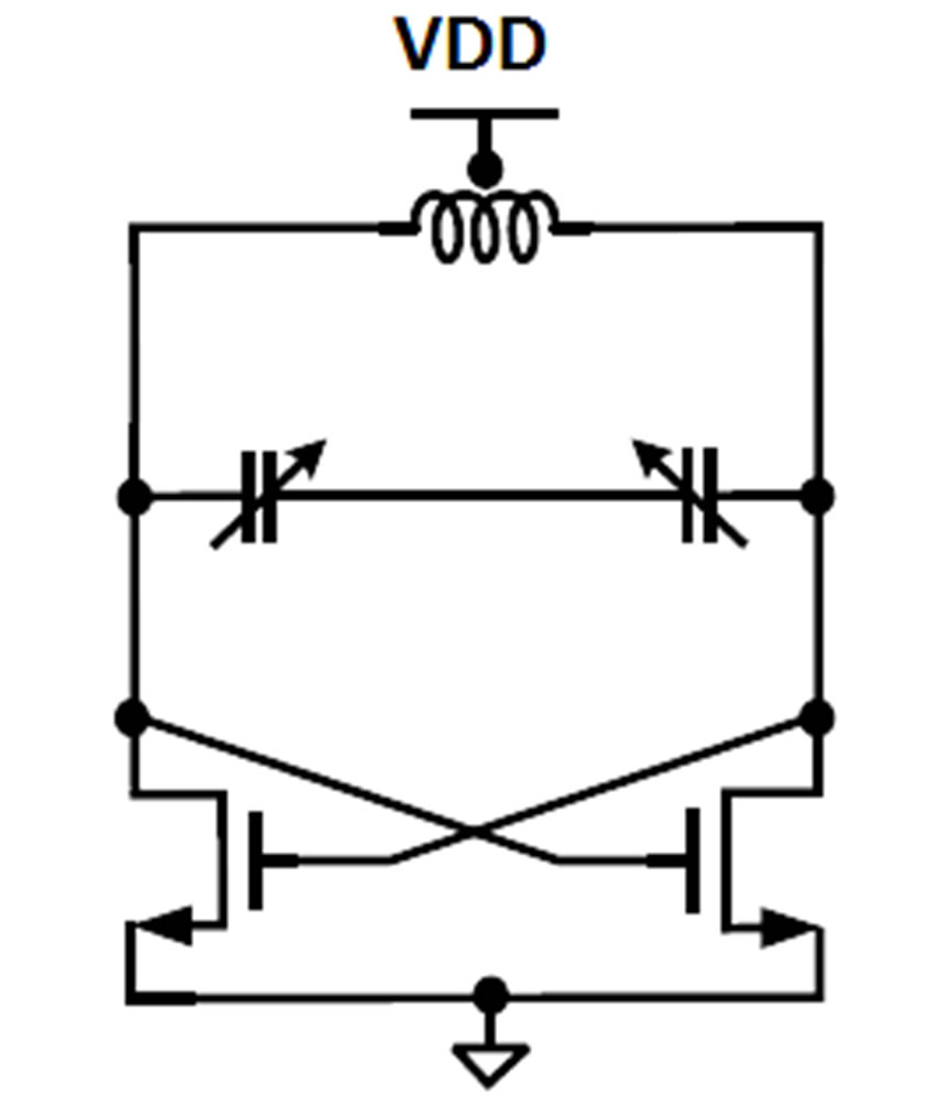
We have demonstrated the availability of oscillations in the subthreshold regime for about 10 GHz oscillation frequency using 0.18 µm CMOS process, which by the best knowledge of the authors, this is the first VCO that has been designed for this range of oscillations that uses the subthreshold biased MOSFETs. Figure 1(a) shows the conventional NMOS only cross coupled deferential VCO structure that is a good candidate for the subthresh-
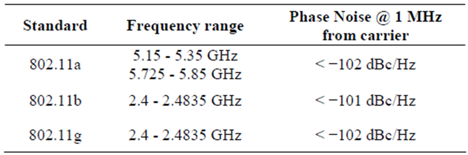
Table 1. WLAN 802.11A/B/G standard specifications [6].
 (a)
(a) (b)
(b)
Figure 1. (a) The conventional cross-coupled NMOS only VCO; (b) The proposed VCO with the extra symmetric inductor for the phase noise reduction.
old operation. The subthreshold biased CMOS transistors in contrast to the super threshold biased transistors exhibit higher gm to power dissipation ratio and comparable noise performance, so the resulting VCO achieves low power and low phase noise characteristics [7].
We use an extra inductor between the source ends of NMOS transistors, Figure 1(b), and will show that it can enhance the phase noise of VCO about 3.5 dB.
The paper is organized as follows. The principles of operation for the subthreshold biased VCO are explained in Section 2. In Section 3, the design procedure of the proposed structure will be explained. The simulation results will be discussed in Section 4. Finally, the conclusions will be presented in Section 5.
2. The Operation of Subthreshold Biased VCO
The drain current of a MOS transistor that is biased in the superthreshold regime (VGS > VTH) is exhibited nearly a square dependence on VGS while biasing in the subthreshold regime (VGS < VTH) changes this dependence to an exponentially relation. As we know in the LC oscillators, although the drain current is important, but its importance originates from the dependence of gm on IDS. The effective negative resistance in oscillators is essentially due to gm variations. Because gm is the derivative of IDS versus VGS, it is clear that its value in the subthreshold regime is about five times greater than that of the superthreshold regime for the same drain current.
For compensating the loss of an LC tank and sustaining the oscillations, we need a minimum negative resistance that is formed by gm of cross-coupled transistors. Thus we can have this minimum gm in the subthreshold region in which the drain current is smaller than the superthreshold condition. Also we can use an NMOS only cross-coupled structure that allows the reduction of supply voltage below the threshold voltage, so the dc power consumption will be decreased more, and the design of an ultra-low power VCO becomes possible.
Phase Noise Considrations in the Subthreshold Regime
The  region in the phase noise characteristics of CMOS oscillators is mainly due to the up-conversion of flicker noise, while in the
  region the thermal noise is dominated [8]. The contribution of passive components with low quality factors on the phase noise degradation of an oscillator, mainly occurs in the
 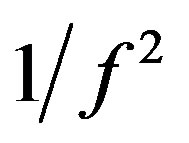 region, while MOS transistors can degrade the phase noise on both
  and
and  regions through their drain current noise.
The drain current noise for a MOS transistor in the superthreshold and subthreshold regimes can be expressed as [9]
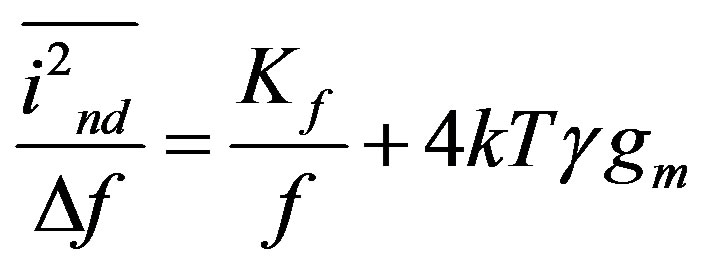 (superthreshold region) (1)
 (subthreshold region) (2)
where Kf is the technology, device and bias dependent parameter, K is the Boltzmann constant, T is the absolute temperature,  is the correction factor, q is the electron charge and IDS is the net drain current. As seen from (1) and (2), the white noise of MOS transistors is dominated by the thermal noise in the superthreshold region, and by the shot noise in the subthreshold region. If both transistors have the same
  values, the shot noise in the subthreshold MOS transistor will be comparable to the thermal noise in the superthreshold one, so the phase noise can be reduced in the
  region.
The flicker noise in both the subthreshold and the superthreshold biased MOS transistors has no significant dependence on the gate voltage and is nearly equal in both regions. Thus, biasing the transistor in the subthreshold regime causes no improvement in the phase noise of oscillator in the  region. However, using the large size MOS transistors leads to lower
  factor values, thus the phase noise in the
  region will be decreased.
In next section, we will describe the design procedure for the new structure to act in the subthreshold region whereas the overall phase noise of oscillator is reduced.
3. Design Procedure
Figure 2 shows the detailed schematicfor the proposed VCO circuit. The cross-coupled nMOSFET pair (M1 and M2) is used to provide the negative differential resistance for compensating the loss of LC tank. Although we can use a complementary structure using an NMOS pair accompanied by a PMOS pair, but for reducing the supply voltage below the threshold voltage and also reducing the dc power dissipation, we prefer to use an NMOS only cross coupled structure. The oscillation frequency of VCO is determined by the LC, which consists of an inductor (L1) and the effective capacitance of circuit. This effective capacitor is composed of the varactor capacitors (Cvar) and all the parasitic capacitors of circuit that are mainly defined by size of the crosscoupled pair. The sizing of transistors and the values of inductor and varactor capacitors have been chosen so that the optimum values for the phase noise and power dissipation and also the optimum tuning range are achieved.
In this design, we use an extra symmetrical center tapped inductor between the source ends of the crosscoupled pairs. Using these inductors we show that the phase noise can be improved about 3.5 dB. Figure 3 shows the phase noise for the proposed VCO structure and the conventional one. It should be noted that, in some designs the designers have used a single ended inductor, e.g. in [7], but not a symmetrical center tapped one used here, stating that it can act as a current source without sacrificing headroom. Here, we explain another aspect of this center tapped inductor. Because of the large signal behaviour of cross-coupled pair in an oscillator, these transistors act as switching MOS transistors and each of them becomes ON and OFF so that they provide an effective negative resistance to compensate the loss of tank and the oscillation will be sustained. On the other hand, we know that the noise of active devices affect the phase noise of oscillator only when they are ON. Thus, if we can sure that when one of the transistors is ON, the other is in the OFF state, the phase noise of oscillator will be reduced. For example, if the gate-source voltage of a transistor becomes negative, it will be OFF so that it cannot even operate in the weak inversion region. For demonstrating these statements, Figure 4 shows the gate-source voltage versus time for this VCO structure. As it is clear, the gate-source voltage becomes negative by using the extra center tapped inductor, whereas without using this inductor, the gate-source voltage can reach to zero for a short time, such that the time duration that the transistor is OFF is much lower than the case before (the extra inductor added to circuit). Therefore, one of the advantages of this extra inductor is that the voltage across it can be lower than the ground, so it can be useful to reduce the phase noise of VCO.
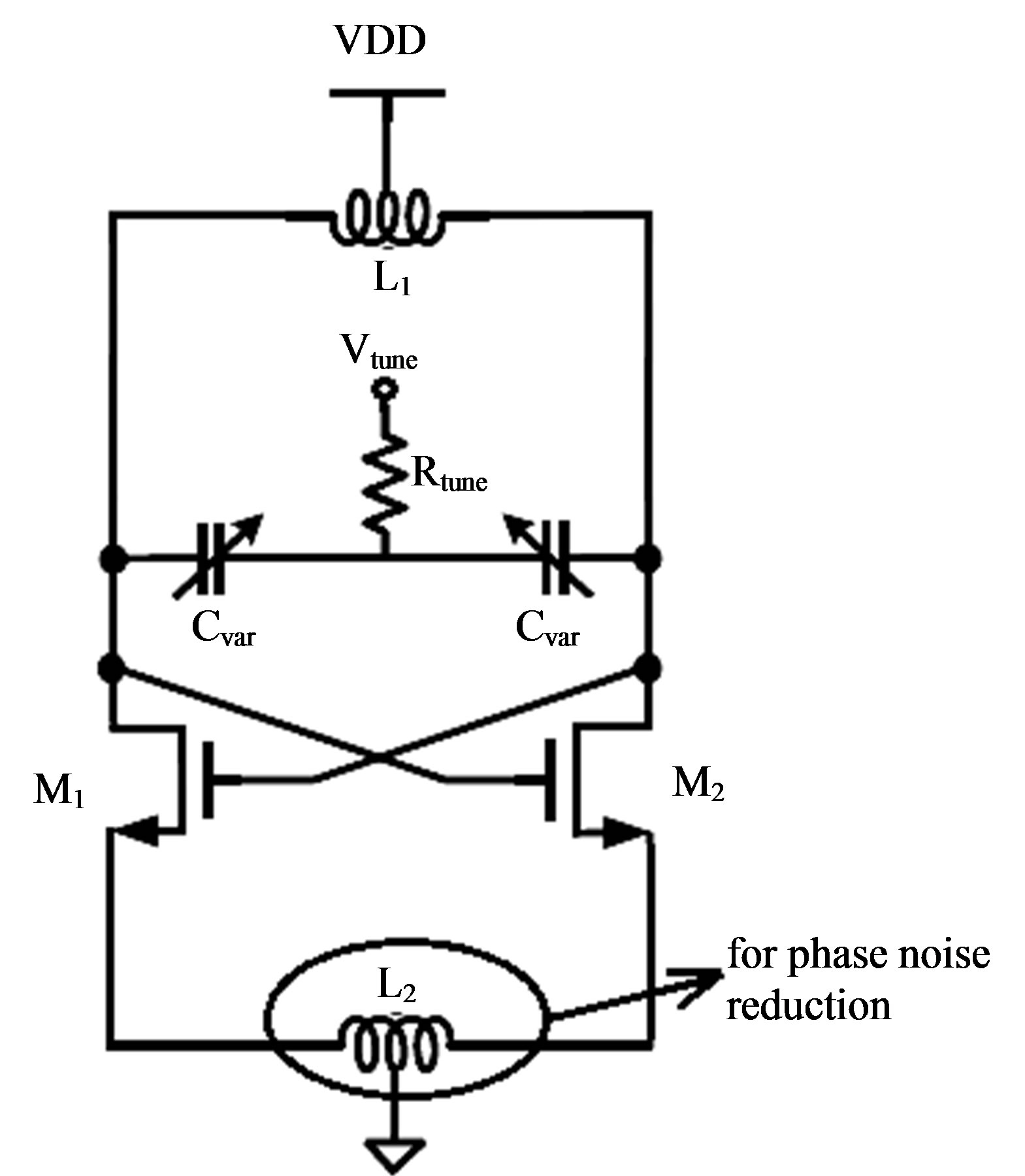
Figure 2. The proposed VCO schematic that uses an extra symmetric inductor between the source ends, for reducing the phase noise.

Figure 3. The simulated phase noise for the proposed VCO structure, with an extra inductor between the source ends of cross-coupled core transistors, and without it.

Figure 4. The transient simulated gate-source voltage of an NMOS in the cross-coupled core of proposed VCO. It shows that with the addition of an extra inductor between the source ends, the time duration that an NMOS remains OFF is increased, thus the phase noise will be improved.
In the design of the discussed oscillator structure we have used the standard components of 0.18 µm CMOS process, and the simulations have been performed using Advanced Design System (ADS) simulator. In the next section, the simulation results will be reported exactly.
To demonstrate the effectiveness of this technique theoretically, this circuit could be treat as a current biased oscillator with the difference that instead of an active current source it uses the expressed inductors. It has been demonstrated in [10] that the analytical phase noise formula for the current biased structure can be expressed as
 (3)
(3)
where k is the Boltzmann constant, T is the absolute temperature, I0 is the current passes through the current source, V1 and R are the peak voltage across the resonator and the loss of LC resonator, respectively. The quality factor and the resonance frequency of the resonator are denoted by Q and ω0, respectively, and ωm denotes the offset frequency from the resonance frequency. The three terms in the right braces express the effect of resonator noise, the differential pair noise and the tail current noise on the total phase noise, respectively. Since in this circuit the tail current source is not an MOS transistor, so the third right-most term in the braces will vanish and consequently the total expression for the phase noise of proposed circuit can be approximately expressed as
 (4)
(4)
which is apparently smaller than the case of a tail biased oscillator.
4. Simulation Results
The proposed VCO structure has been designed in the TSMC 0.18 µm CMOS process technology. The core of proposed VCO consumes 0.346 mW dc power, under the power supply of 0.46 V and with . Figure 3 shows the simulated phase noise for the proposed VCO structure, with an extra inductor between the source ends of cross-coupled core transistors, and also the results for the case that it has been omitted. As it is clear from this figure, the phase noise of proposed VCO is −107.82 dBc/Hz at 1 MHz offset frequency, whereas without using the mentioned extra inductor, the phase noise will be −104.32 dBc/Hz, i.e. nearly 3.5 dB increase for the latter case. This result demonstrates that by cost of area, we can achieve a better phase noise performance by adding an extra inductor as mentioned.
As mentioned in the previous sections, the phase noise faces 3.5 dB improvements by adding the extra inductor at the source of differential pair. It is clear from Figure 3 that, the presence of inductor causes the source nodes of differential pair actually float below the ground, since their ground connection is made through the inductor. Therefore, the gate-source voltage of differential pair in some moments can be negative and consequently lowers the phase noise. This effect can be viewed from another point of view. As we know, the linearity of VCO can reduce the phase noise; therefore, the source degeneration technique with inductor (which is a usual technique for the linearity improvement in LNAs) can enhance the linearity and further improve the phase noise.
As shown in Figure 5, the oscillation frequency can be tuned from 10.53 GHz to 10.88 GHz with the tuning voltage varying from 0 to 0.5 V. As the control voltage is increased to 1.8 V, the oscillation frequency becomes 11.35 GHz so that the tuning range will be about 0.8 GHz or 7.5%.
The figure of merit (FOM) for the VCO structure is defined as [11]
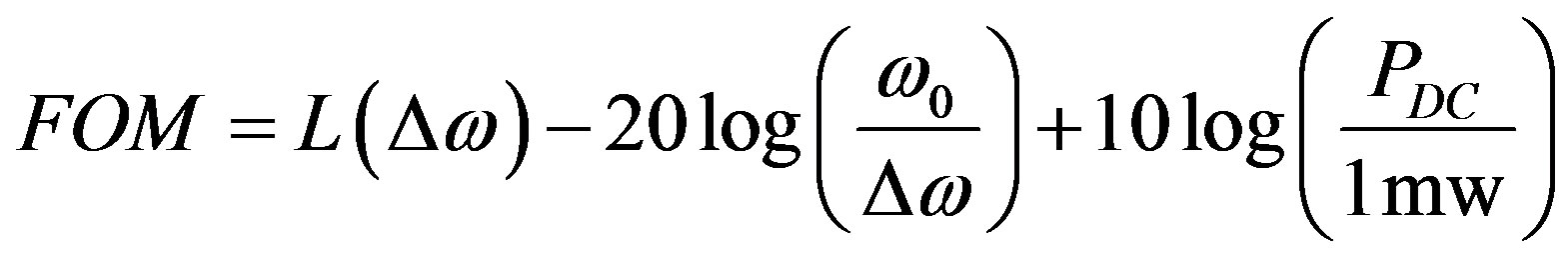 (5)
(5)
where  is the phase noise at the offset frequency
 ,
,  is the oscillation frequency, and
  is the dc power consumption of oscillator. The calculated FOM for the proposed VCO using (5) is −193.18 dBc/Hz.
Table 2 summarizes the state of the art and compares the performance parameters for the ultra-low power and low phase noise VCO designs, between our proposed structure and some different references. As cleared from this table, all of designs in the mentioned references have oscillation central frequencies below 5 GHz and by the best knowledge of the authors, the proposed structure is the first oscillator which has been designed in the subthreshold regime at the frequency of 10 GHz and beyond.
5. Conclusion
In this paper, we have proposed a new design for an ultra-low power and low phase noise 10 GHz LC VCO, which uses an NMOS only cross-coupled pair and is biased in the subthreshold regime. Due to the subthreshold biasing, the dc power dissipation has been decreased greatly so that the VCO dissipates only 0.346 mW under 0.46 V power supply. By adding an extra inductor to the conventional structure of cross-coupled VCO, as in Figure 2, we can achieve a 3.5 dB improvement in the phase noise. Regarding this achievement, the VCO will have a phase noise of −107.8 dBc/Hz at 1MHz from the oscillation frequency of 10.53 GHz. Also the oscillation frequency can be varied from 10.53 GHz to 11.35 GHz,
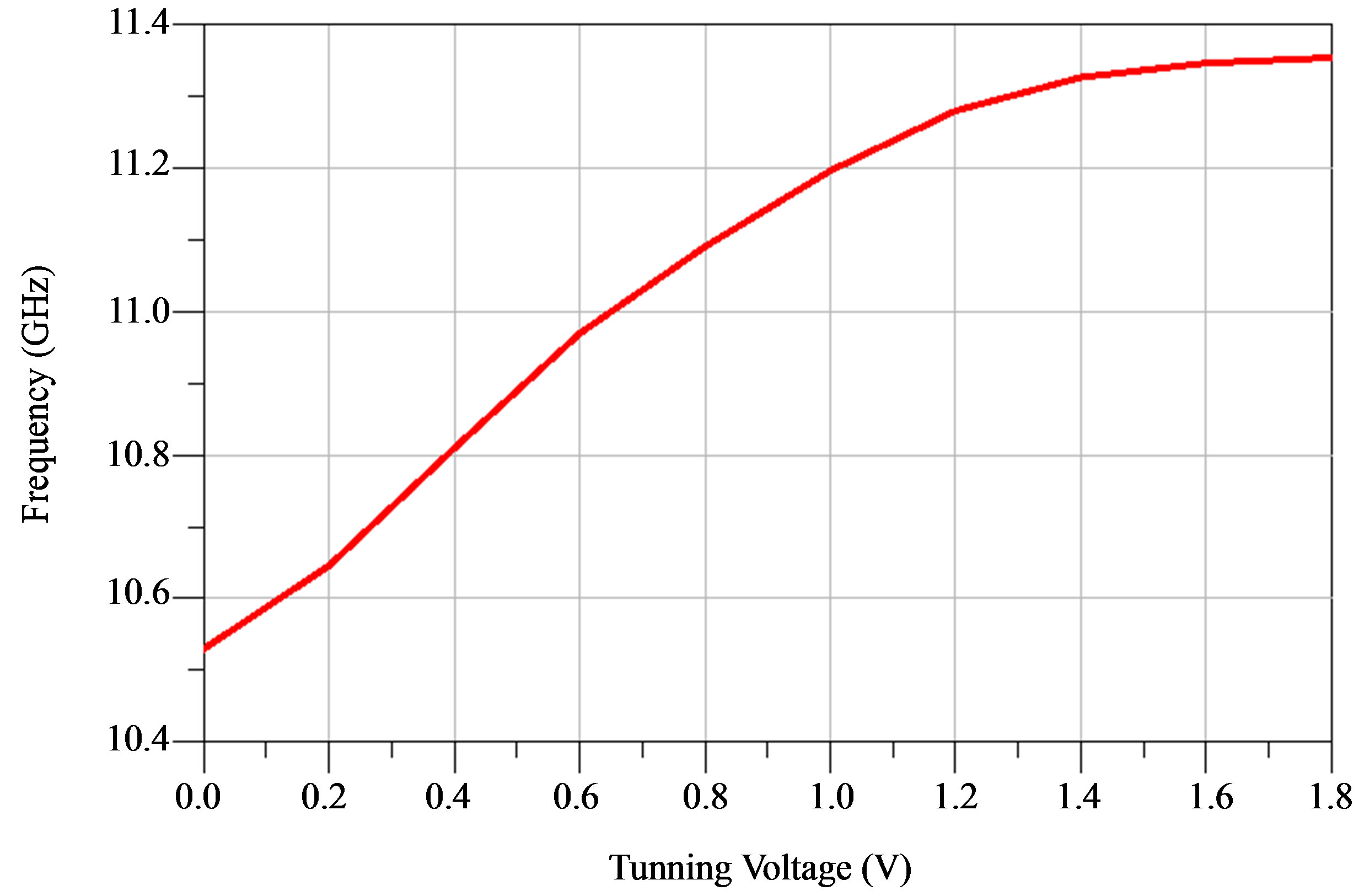
Figure 5. The simulated tuning range for the proposed VCO structure. The proposed VCO circuit achieves a tuning range of 7.5%.
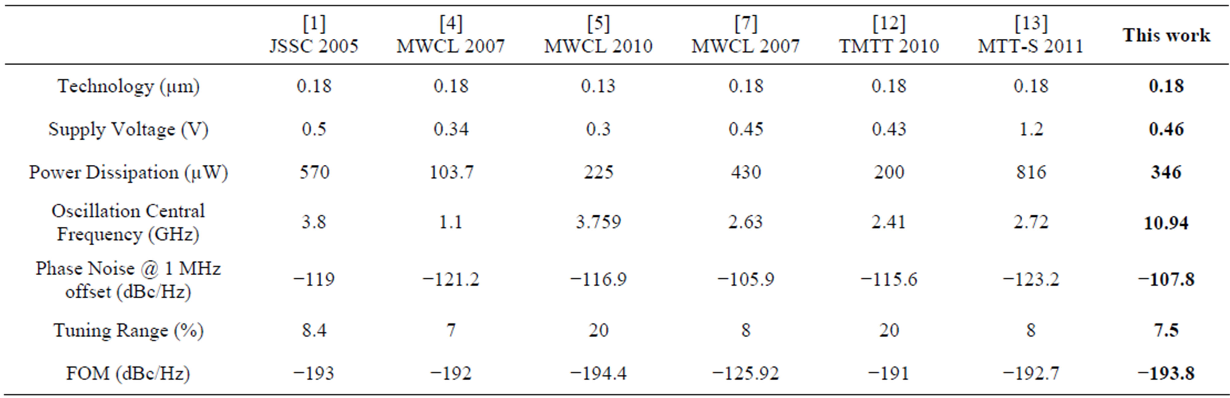
Table 2. Performance comparison.
Which gives 7.5% tuning range. On the other hand, the proposed VCO shows a figure of merit equal to −193.8 dB using (5), which by the best knowledge of authors, is the first VCO structure which has been designed in subthreshold regime at the mentioned oscillation frequency. It should be noted that, this new VCO can be used in the multi-standard wireless LAN communication protocols 802.11a/b/g easily by a frequency division of 2 or 4, respectively.
REFERENCES
- K. Kwok and H. C. Luong, “Ultra-Low-Voltage HighCMOS VCOs Using Transformer Feedback,” IEEE Journal of Solid-State Circuits, Vol. 40, No. 3, 2005, pp. 652-660. doi:10.1109/JSSC.2005.843614
- J. Jaeyoung, Z. Siqi, L. Peng, Y. E. Chen and H. Deukhyoun, “22-pJ/bit Energy-Efficient 2.4-GHz Implantable OOK Transmitter for Wireless Biotelemetry Systems: In Vitro Experiments Using Rat Skin-Mimic,” IEEE Transactions on Microwave Theory and Echniques, Vol. 58, No. 12, 2010, pp. 4102-4111.
- O. Nam-Jin and L. Sang-Gug, “Current Reused LC VCOs,” IEEE Microwave and Wireless Components Letters, Vol. 15, No. 11, 2005, pp. 736-738. doi:10.1109/LMWC.2005.858993
- S. L. Jang and C.-F. Lee, “A Low Voltage and Power LC VCO Implemented with Dynamic Threshold Voltage MOSFETS,” IEEE Microwave and Wireless Components Letters, Vol. 17, No. 5, 2007, pp. 376-378. doi:10.1109/LMWC.2007.895720
- S.-L. Jang, C.-J. Huang, C.-W. Hsue and C.-W. Chang, “A 0.3 V Cross-Coupled VCO Using Dynamic Threshold MOSFET,” IEEE Microwave and Wireless Components Letters, Vol. 20, No. 3, 2010, pp. 166-168. doi:10.1109/LMWC.2010.2040220
- M. Brandolini, P. Rossi, D. Manstretta and F. Svelto, “Toward Multistandard Mobile Terminals—Fully Integrated Receivers Requirements and Architectures,” IEEE Transactions on Microwave Theory and Techniques, Vol. 53, No. 3, 2005, pp. 1026-1038. doi:10.1109/TMTT.2005.843505
- L. Hanil and S. Mohammadi, “A Subthreshold Low Phase Noise CMOS LC VCO for Ultra Low Power Applications,” IEEE Microwave and Wireless Components Letters, Vol. 17, No. 11, 2007, pp. 796-798. doi:10.1109/LMWC.2007.908057
- A. Hajimiri and T. H. Lee, “A General Theory of Phase Noise in Electrical Oscillators,” IEEE Journal of SolidState Circuits, Vol. 33, No. 2, 1998, pp. 179-194. doi:10.1109/4.658619
- H.-F. Teng, S.-L. Jang and M. H. Juang, “A Unified Model for High-Frequency Current Noise of MOSFETs,” Solid-State Electronics, Vol. 47, No. 11, 2003, pp. 2043- 2048. doi:10.1016/S0038-1101(03)00248-X
- E. Hegazi, J. Rael and A. Abidi, “The Designer’s Guide to High-Purity Oscillators,” Springer, Berlin, 2004.
- C.-Y. Jeong and C. Yoo, “5-GHz Low-Phase Noise CMOS Quadrature VCO,” IEEE Microwave Wireless Components Letters, Vol. 16, No. 11, 2006, pp. 609-611. doi:10.1109/LMWC.2006.884908
- P. Dongmin and C. SeongHwan, “Design Techniques for a Low-Voltage VCO with Wide Tuning Range and Low Sensitivity to Environmental Variations,” IEEE Transactions on Microwave Theory and Techniques, Vol. 57, No. 4, 2009, pp. 767-774.
- J. Jaeyoung, P. Upadyaya, L. Peng and H. Deukhyoun, “Compact Sub-1mW Low Phase Noise CMOS LC-VCO Based on Power Reduction Technique,” 2011 IEEE MTTS International Microwave Symposium Digest (MTT), Baltimore, 5-10 June 2011, pp. 1-4.
NOTES
*Corresponding author.