Circuits and Systems
Vol. 4 No. 2 (2013) , Article ID: 29850 , 10 pages DOI:10.4236/cs.2013.42020
Performance Evaluation of Efficient XOR Structures in Quantum-Dot Cellular Automata (QCA)
Department of Electronics & Instrumentation Technology, University of Kashmir, Srinagar, India
Email: *mrbku@yahoo.com
Copyright © 2013 Mohammad Rafiq Beigh et al. This is an open access article distributed under the Creative Commons Attribution License, which permits unrestricted use, distribution, and reproduction in any medium, provided the original work is properly cited.
Received December 4, 2012; revised January 14, 2013; accepted January 22, 2013
Keywords: Nanoelectronics; Quantum Cellular Automata (QCA); Majority Logic; Combinational Logic; XOR Gate; QCA Designer
ABSTRACT
Quantum-dot cellular automaton (QCA) is an emerging, promising, future generation nanoelectronic computational architecture that encodes binary information as electronic charge configuration of a cell. It is a digital logic architecture that uses single electrons in arrays of quantum dots to perform binary operations. Fundamental unit in building of QCA circuits is a QCA cell. A QCA cell is an elementary building block which can be used to build basic gates and logic devices in QCA architectures. This paper evaluates the performance of various implementations of QCA based XOR gates and proposes various novel layouts with better performance parameters. We presented the various QCA circuit design methodology for XOR gate. These layouts show less number of crossovers and lesser cell count as compared to the conventional layouts already present in the literature. These design topologies have special functions in communication based circuit applications. They are particularly useful in phase detectors in digital circuits, arithmetic operations and error detection & correction circuits. The comparison of various circuit designs is also given. The proposed designs can be effectively used to realize more complex circuits. The simulations in the present work have been carried out using QCADesigner tool.
1. Introduction
Quantum-dot cellular automata (QCA) is an emerging nanoelectronic technology that offers a revolutionary approach to computing at nano level [1]. A very extensive research and development in the field device technology for the past several decades made it possible for designers and processing engineers rapidly and consistently reduce semiconductor device size and operating current. But the incessant development in device fabrication on the nanometer scale is limited not only by process technology, but also by fundamental problems arising from scaling, such as quantum-mechanical effects and severe power dissipation. In MOS devices the gate tunneling current increases with the future size going down to deep submicron device geometry process. As a result the device and circuit characteristics drastically are deviated from the designer’s expectations of making it better suited from application point of view. Further, in several studies it is predicted that these device technologies are approaching to its physical limits [2-4]. Any physical phenomenon that has two separate states can be used to express a logic variable in two valid logic states such as electronic spin. Quantum effect is preferred to utilize in representing logic rather than any other method. Quantum logic devices are presented under this consideration and one of these is known as Quantum-dot Cellular Automata [5,6]. QCA is an emerging paradigm which allows operating frequencies in the range of THz and device integration densities about 900 times than the current end of CMOS scaling limits. It has been predicted as one of the future nanotechnologies in Semiconductor Industries Association’s International Technology Roadmap for Semiconductors (ITRS) [7]. QCA based circuits have an advantage of high speed, high integrity and low power consumption [8,9]. Also QCA circuits have an advantage of high parallel processing [10,11]. Recent work showed that QCA can achieve high density, fast switching speed, and room temperature operation [12,13]. In recent years various QCA based combinational circuit designs have been proposed [14-19] but comparatively less study efforts have been made with its application in the field of communication. We present here different layouts of QCA based XOR structures that can be used in design and development of specific communication circuits, like parity generators & checkers, error detection & correction circuits and LFSRs. These designs are efficient in terms of cell count, complexity and latency as compared to the already proposed designs. These designs follow the conventional design approach but due to the technology differences, they are modified for the best performance in QCA.
In this paper we propose the seven novel implementations of the QCA based XOR gate and presented the simulation results of these individual designs. A detail comparison with regard to various characteristics of these designs is also presented. The paper has been organized in five sections. The first and second section provides the necessary introduction and review of QCA fundamentals. The third section presents the conventional XOR implementations. The various novel QCA XOR topologies have been presented in the fourth section. The advantages of the proposed structures have been summed up as conclusion in the fifth section.
2. QCA Fundamentals
In this section, we briefly describe the preliminaries of QCA and computation mechanism using QCA cells.
2.1. Basic QCA Cell
A QCA cell is a structure comprised of four quantumdots arranged in a square pattern as shown in Figure 1. These quantum-dots are sites in which electrons are able to tunnel between them but cannot leave the cell.
QCA information processing is based on the Columbic interactions between many identical QCA cells. Each QCA cell is constructed using four electronic sites or dots coupled through quantum mechanical tunneling barriers. The electronic sites represent locations that a mobile electron can occupy. The cells contain two mobile electrons (or holes) which repel each other as a result of their mutual Columbic interaction, and, in the ground state, tend to occupy the diagonal sites of the cell. Therefore the cell has two degenerate ground states. These lead to two polarizations of a QCA cell, denoted as P = +1 and P = −1 respectively. Binary information can be encoded in the polarization of electrons in each QCA cell. Thus, logic 0 and logic 1 are encoded in polarization P = −1 and P = +1 respectively. Figure 1 also shows the two possible polarizations of a QCA cell. Binary computation requires interaction among bits, in these devices, among the cells. When a second cell is placed near the first cell, the coulomb interaction between the cells removes the degeneracy and determines the ground state of the first

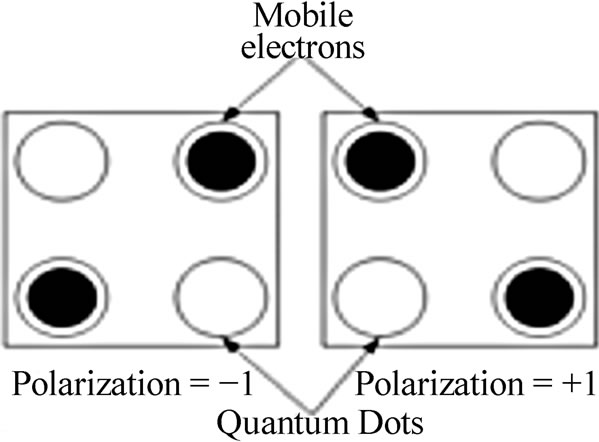
Figure 1. QCA cell and polarizations of QCA cell.
cell. The interaction between the QCA cells is nonlinear that is with a small perturbation from a neighboring cell clicks it into essentially aligned configuration either with P = +1 or P = −1 as will be the appropriate.
2.2. QCA Wires
In a QCA wire, the binary signal propagates from input to output because of the electrostatic interactions between cells. The propagation in a 90˚ QCA wire is shown in Figure 2(a). Other than the 90˚ QCA wire, a 45˚ QCA wire can also be used as shown Figure 2(b). In this case, the propagation of the binary signal alternates between the two polarizations [5].
2.3. QCA Majority Gate and Inverter
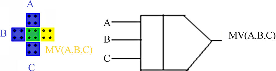
The fundamental QCA logical circuit is the three-input majority gate that appears in Figure 3 [5]. The majority gate produces an output that reflects the majority of the in A puts.
The QCA majority gate has four terminal cells out of which three are representing input terminals and the remaining one represents the output cell [5]. Assuming that the three inputs are A, B and C, the logic function of the majority gate is

The two different structures of QCA inverter is shown in Figure 4. An inverter is usually formed by placing the cells with only their corners touching. The electrostatic interaction is inverted, because the quantum dots corresponding to different polarizations are misaligned between the cells [20]. The second inverter is built by neighboring QCA cells on the diagonal, which causes Coulomb forces to place the two electrons in opposing wells of the cell with respect to the source.
The AND and OR logic is realized by fixing the polarization of one of the inputs of the majority gate to either P = −1 (logic “0”) or P = 1 (logic “1”) as shown in
 (a)
(a) (b)
(b)
Figure 2. (a) QCA wire (90˚); (b) QCA wire (45˚).
 (a) (b)
Figure 3. (a) QCA majority gate; (b) Schematic majority gate representation.
 (a) (b)
Figure 4. QCA inverters.
The NAND function is realized by connecting AND gate (MG) followed by an inverter. By using this 2 cell inverter, the area required and complexity can be minimized. The layout and schematic is shown in Figure 6.
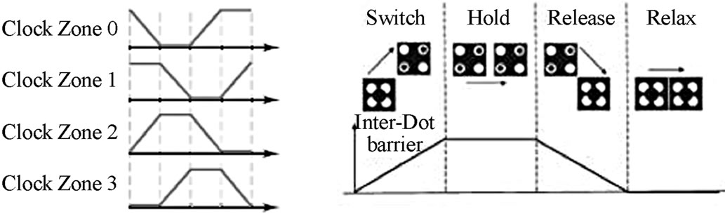
2.4. QCA Clocking
The QCA circuits require a clock, not only to synchronize and control information flow but also to provide the power to run the circuit since there is no external source for powering cells. The clocking of QCA can be accomplished by controlling the potential barriers between adjacent quantum-dots [21,22]. With the use of four phase clocking scheme in controlling cells, QCA processes and forwards information within cells in an arranged timing scheme. Cells can be grouped into zones so that the field influencing all the cells in the zones will be the same. Figure 7(a) shows the four phases of QCA clock. Figure 7(b) shows the four available clock signals. Each signal is phase shifted by 90˚ degrees. In the Switch phase, the tunneling barriers in a zone are raised. While this occurs, the electrons within the cell can be influenced by the Columbic charges of neighboring zones. Zones in the Hold phase have a high tunneling barrier and will not change state, but influence other adjacent zones. Lastly, the Release and Relax decrease the tunneling barrier so that the zone will not influence other zones. These zones can be of irregular shape, but their size must be within certain limits imposed by fabrication and dissipation concerns. Proper placement of these zones is critical to design efficiency.

Figure 5. QCA layout of AND, OR gate.
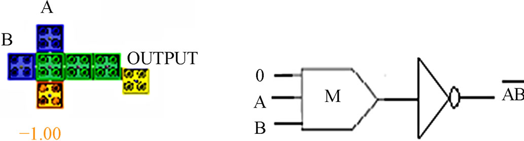
Figure 6. QCA layout of NAND gate.
 (a) (b)
Figure 7. The four phases of the QCA clock.
This clocking method makes the design of QCA different from CMOS circuits.
Each signal is phase shifted by 90˚ degrees. When the clock signal is low the cells are latched. When the clock signal is high the cells are relaxed and have no polarization. In between the cells are either latching or relaxing when the clock is decreasing/increasing respectively.
3. QCA Exclusive-OR Implementations
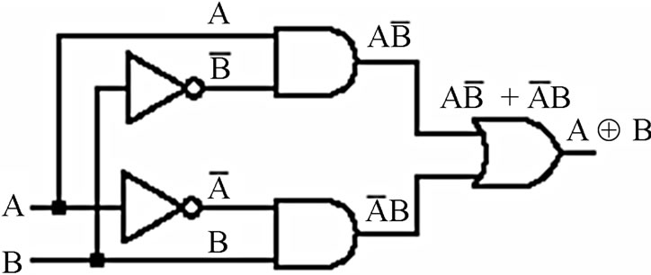
In addition to AND, OR, NOT, NAND and NOR gates, exclusive-OR (XOR) and exclusive-NOR (XNOR) gates are also used in the design of digital circuits. These have special functions and applications. These gates are particularly useful in arithmetic operations as well as errordetection and correction circuits. XOR and XNOR gates are usually found as 2-input gates. No multiple-input XOR/XNOR gates are available since they are complex to fabricate with hardware.
The exclusive-OR (XOR) performs the following logic operation:

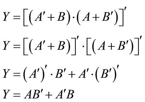
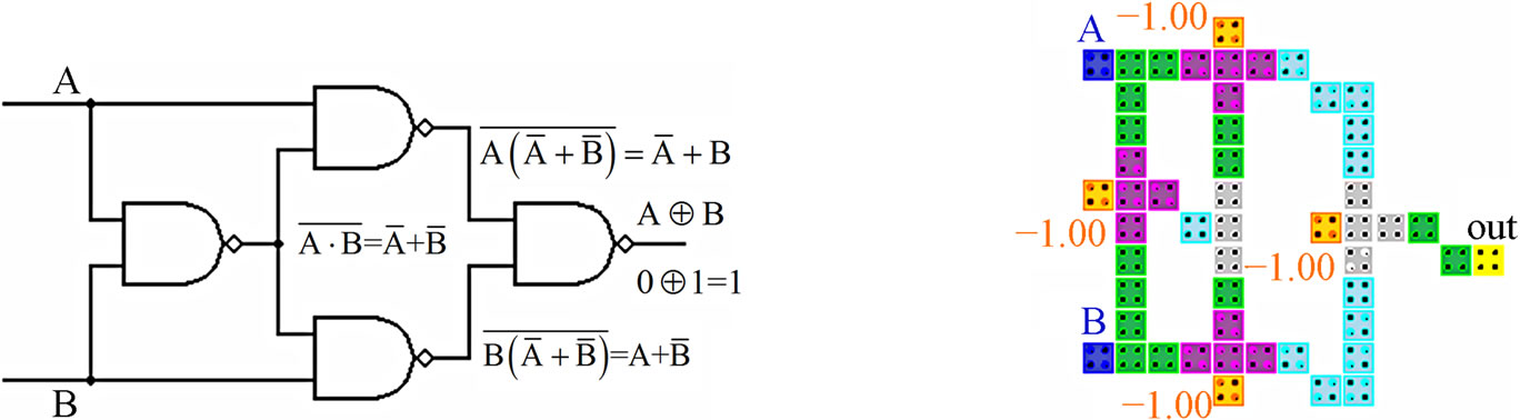
The conventional schematic representation of XOR and two different QCA implementations for this layout is shown in Figure 8.
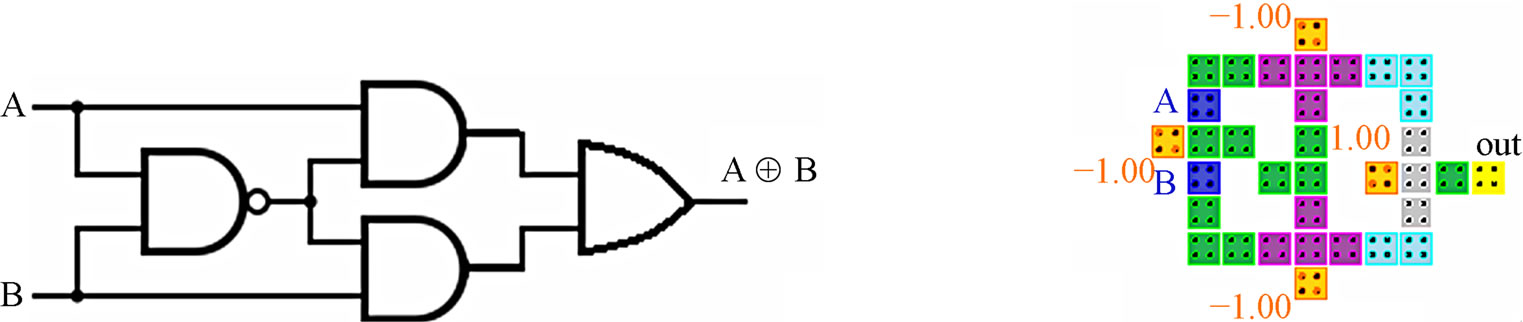
The QCA implementation for the layout shown in Figure 8(a) has been proposed by different authors [5,23]. This design needs either coplanar crossovers or multiple layers to implement. The design provided as a sample file with QCA Designer Version 2.0.3 [24] needs cross-
 (a)
(a)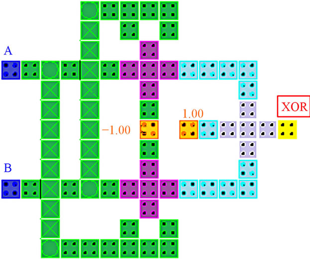 (b)
(b) (c)
(c)
Figure 8. Conventional QCA-XOR schematic & implementation.
overs and uses three layers to implement. This design is shown in Figure 8(b). We have proposed in this work seven different QCA based designs of XOR. These layouts have been designed to provide the more efficient configurations in terms of cell count, latency and complexity.
4. Proposed XOR Structures
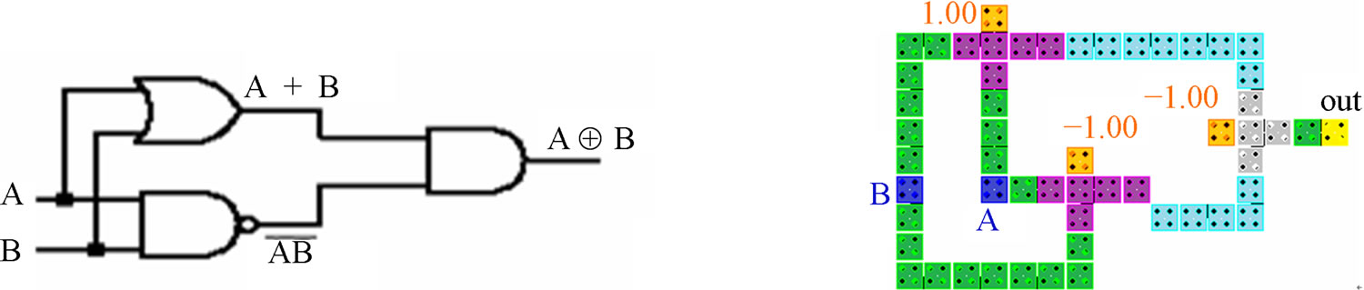
Exclusive OR, also known as Exclusive disjunction and symbolized by XOR, is a logical operation on two operands that results in a logical value of true if and only if one of the operands, but not both, has a value of true. This forms a fundamental logic gate in many operations. An XOR gate can be trivially constructed from an XNOR gate followed by a NOT gate. We can construct an XOR gate directly using AND, OR and NOT gates. However, this approach requires five gates of three different kinds. Logically, the exclusive OR (XOR) operation can also be implemented by the gate arrangements to follow. For instance they can also be implemented using NAND or NOR gates only.
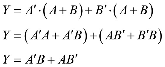
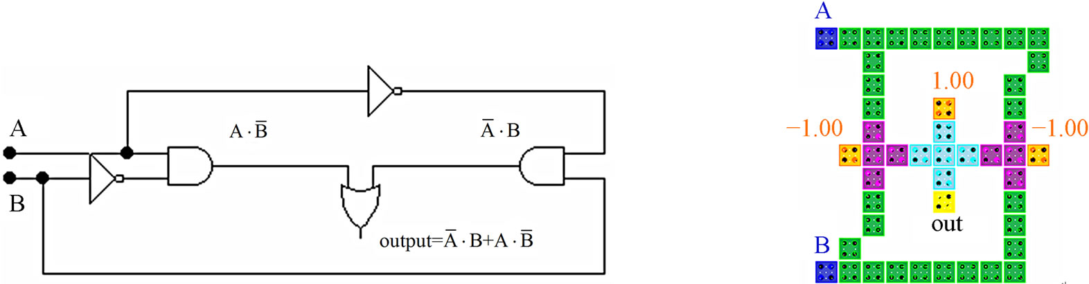
4.1. The First Design
Every Boolean function can be build from (binary) Fred kin Gates (FGs), such that it has two inputs A, B and one output Y. The first design is based on Equation (1) which can be simplified as
 (1)
(1)
The proposed QCA XOR gate has no crossovers and has cell count of 34 cells and an area of approximately 0.06 um2 which is less as compared to conventional layouts. The proposed layout of this design and simulation results are shown in Figures 9 (b) and (c).
4.2. The Second Design
The second design is based on Equation (2) which can be reduced to basic XOR equation as shown below.
 (2)
(2)
The proposed QCA XOR gate will require one crossover in order to input “A” separately out of the gate. It has cell complexity of 54 cells and an area of approximately 0.07 um2. The proposed QCA layout of this XOR gate and simulation results are shown in Figures 10(b) and (c).
4.3. The Third Design
The third design is based on Equation (3) which can be simplified as
 (3)
(3)
The QCA layout and simulation results of this design
 (a)
(a)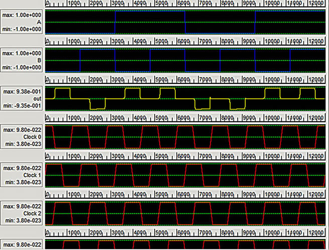 (b)
(b)
Figure 9. First proposed QCA XOR gate and simulation results.
 (a)
(a) (b)
(b)
Figure 10. 2nd proposed QCA XOR gate and simulation results.
are shown in Figures 11(b) and (c) respectively. The proposed QCA XOR gate does not require any crossover. It has cell complexity of 52 cells and an area of approximately 0.08 um2. It has a latency of two clock cycles.
4.4. The Fourth Design
The fourth design is based on Equation (4) which can be simplified as
 (4)
(4)
The proposed QCA design has a latency of 2 clock cycles and an area of 0.09 and cell count of 52 cells. It does not require any crossover. The proposed QCA gate and its simulation results are also shown in Figure 12.
4.5. The Fifth Design
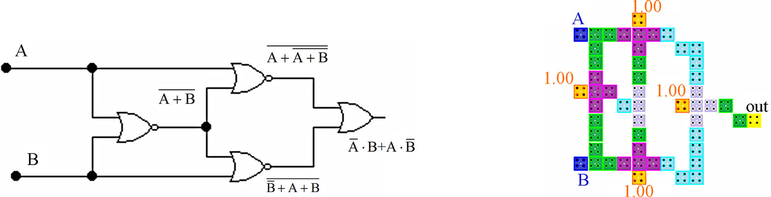
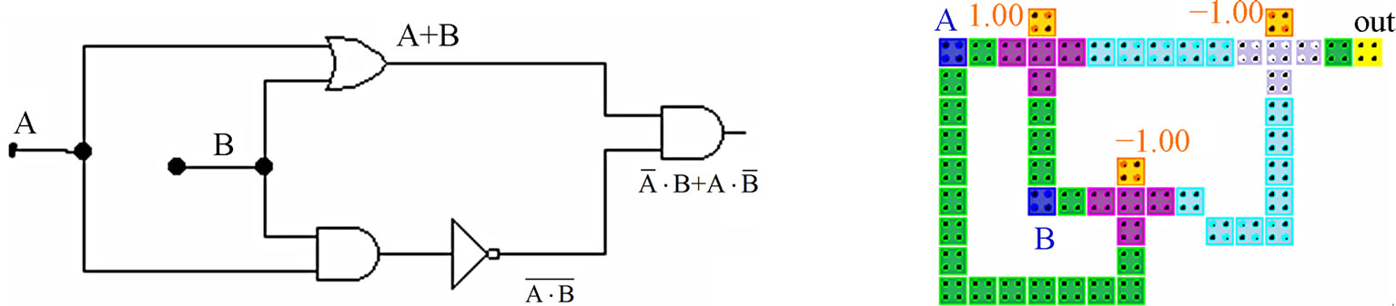
The fifth design is based on the gate arrangement shown in Figure 13(a). It will require one crossover in order to output “out” separately out of the gate.
The proposed QCA design has a latency of  clock cycles and an area of 0.06 and has a cell count of 48 cells. The QCA layout of this gate and its simulation results are also shown in Figure 13.
4.6. The Sixth Design
The sixth design is based on the gate arrangement shown in Figure 14(a).
The QCA layout and simulation results of this design are shown in Figures 14(b) and (c) respectively. This design has a latency of 1 clock cycle and an area of 0.07 um2. It has a cell count of 54 cells.
4.7. The Seventh Design
The seventh design is based on the gate arrangement shown in Figure 15(a).
The proposed QCA design has a latency of  delays and an area of 0.05 and circuit complexity of 42 cells. The proposed QCA gate and simulation results are shown in Figures 15(b) and (c) respectively.
5. Conclusions
In this paper we have proposed efficient structures of Quantum-dot Cellular Automata based XOR gates with reduced number of QCA cells and area compared to previous designs. The proposed designs have been tested and simulated using Bistable Approximation simulation engine of QCA Designer version 2.0.3. The function of the Exclusive OR gate has been verified according to the truth table. These structures were designed with mini-
 (a)
(a)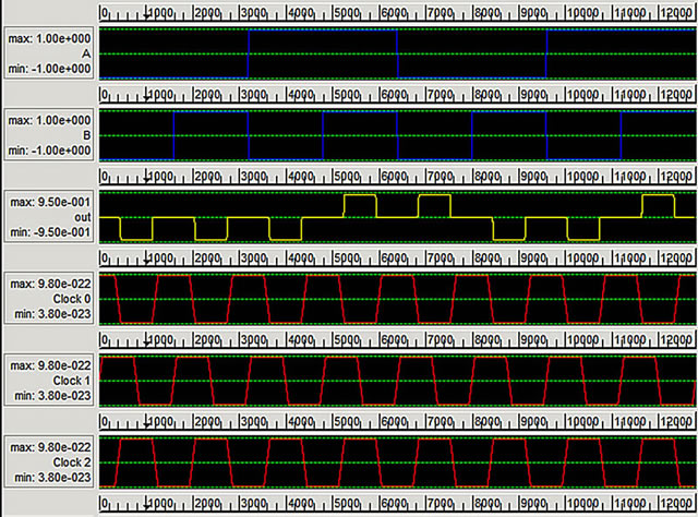 (b)
(b)
Figure 11. 3rd proposed QCA XOR gate and simulation results.
 (a)
(a)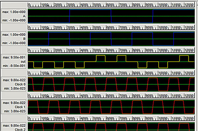 (b)
(b)
Figure 12. 4th proposed QCA XOR gate and simulation results.
 (a)
(a) (b)
(b)
Figure 13. 5th proposed QCA XOR gate and simulation results.
 (a)
(a) (b)
(b)
Figure 14. 6th proposed QCA XOR gate and simulation results.
 (a)
(a)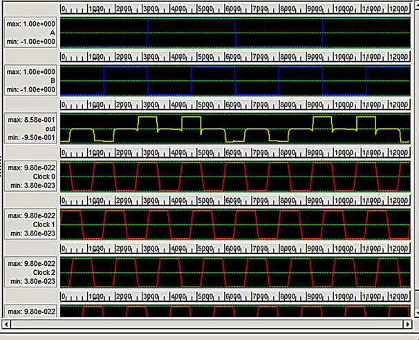 (b)
(b)
Figure 15. 7th proposed QCA XOR gate and simulation results.

Table 1. Comparison of logical structures.
mum number of cells by using cell minimization techniques. The area and complexity are the major issues in QCA circuit design. The proposed technique can be used to minimize area and complexity.
Table 1 gives the comparison of proposed designs with that of conventional designs as shown in Figure 8. It is evident from Table 1 that the proposed designs are efficient in terms of cell count, area and cross-overs (number of layers).
The proposed layouts can be easily used to design complex circuits based on XOR operation like parity generator and checker circuits, PN sequence generators, Linear Block Code circuits and Linear Feedback Shift Registers.
REFERENCES
- C. S. Lent, P. D. Tougaw, W. Porod and G. H. Bernstein, “Quantum Cellular Automata,” Nanotechnology, Vol. 4, No. 1, 1993, pp. 49-57. doi:10.1088/0957-4484/4/1/004
- Y. Kim, “Challenges for Nanoscale MOSFETs and Emerging Nanoelectronics,” Transaction on Electrical and Electronic Materials, Vol. 11, No. 3, 2010, pp. 93-105. doi:10.4313/TEEM.2010.11.3.093
- Y. Taur, “CMOS Design near the Limit of Scaling,” IBM Journal of Research & Development, Vol. 46, No. 2, 2002, pp. 213-222. doi:10.1147/rd.462.0213
- D. J. Frank, “Power-Constrained CMOS Scaling Limits,” IBM Journal of Research & Development, Vol. 46, No. 2, 2002, pp. 235-244. doi:10.1147/rd.462.0235
- P. D. Tougaw and C. S. Lent, “Logical Devices Implemented Using Quantum Cellular Automata,” Journal of Applied Physics, Vol. 75, No. 3, 1994, pp. 1818-1825. doi:10.1063/1.356375
- A. O. Orlov, I. Amlani, G. H. Bernstein, C. S. Lent and G. L. Snider, “Realization of a Functional Cell for Quantum-Dot Cellular Automata,” Science, Vol. 277, No. 5328, 1997, pp. 928-930. doi:10.1126/science.277.5328.928
- International Technology Roadmap for Semiconductors (ITRS), 2004. http://www.itrs.net/Links/2004Update/2004Update.htm
- C. G. Smith, “Computation without Current,” Science, Vol. 284, No. 5412, 1999, pp. 274-274. doi:10.1126/science.284.5412.274
- J. Timler and C. S. Lent, “Power Gain and Dissipation in Quantum-Dot Cellular Automata,” Journal of Applied Physics, Vol. 91, No. 2, 2002, pp. 823-831. doi:10.1063/1.1421217
- D. A. Antonelli, et al., “Quantum-Dot Cellular Automata (QCA) Circuit Partitioning: Problem Modeling and Solutions,” Proceedings of the 41st ACM/IEEE Design Automata Conference, 2004, pp. 363-368.
- M. T. Niemier and P. M. Kogge, “Exploring and Exploiting Wire-Level Pipelining in Emerging Technologies,” ACM SIGARCH Computer Architecture News, Vol. 29, No. 2, 2001, pp. 166-177. doi:10.1145/384285.379261
- B. Isaksen and C. S. Lent, “Molecular Quantum-Dot Cellular Automata,” Proceedings of the Third IEEE Conference on Nanotechnology, Vol. 2, 2003, pp. 5-8.
- C. S. Lent and B. Isaksen, “Clocked Molecular Quantum-Dot Cellular Automata,” IEEE Transactions on Electron Devices, Vol. 50, No. 9, 2003, pp. 1890-1896. doi:10.1109/TED.2003.815857
- M. Z. Moghadam and K. Navi, “Ultra-Area-Efficient Reversible Multiplier,” Microelectronics Journal, Vol. 43, No. 6, 2012, pp. 377-385. doi:10.1016/j.mejo.2012.02.004
- K. Navi, H. H. Sajedi, R. F. Mirzaee, M. H. Moaiyeri, A. Jalali and O. Kavehei, “High-Speed Full Adder Based on Minority Function and Bridge Style for Nanoscale,” Integration, the VLSI Journal, Vol. 44, No. 3, 2011, pp. 155-162.
- M. M. Arjmand, M. Soryani, K. Navi and M. A. Tehrani, “A Novel Ternary-to-Binary Converter in Quantum-Dot Cellular Automata,” IEEE Computer Society Annual Symposium on VLSI (ISVLSI), Amherst, 19-21 August 2012, pp. 147-152.
- M. Hayati and A. Rezaei, “Design and Optimization of Full Comparator Based on Quantum-Dot Cellular Automata,” ETRI Journal, Vol. 34, No. 2, 2012, pp. 284-287. doi:10.4218/etrij.12.0211.0258
- S. Karthigai Lakshmi and G. Athisha, “Design and Analysis of Subtractors Using Nanotechnology Based QCA,” European Journal of Scientific Research, Vol. 53, No. 4, 2011, pp. 524-532.
- L. Lu, W. Q. Liu, M. O’Neill and E. E. Swartzlander, “QCA Systolic Array Design,” IEEE Transactions on Computers, December 2011.
- W. J. Townsend and J. A. Abraham, “Complex Gate Implementations for Quantum Dot Cellular Automata,” Proceedings of the 4th IEEE Conference of Nanotechnology, Munich, 17-19 August 2004, pp. 625-627.
- G. Snider, A. Orlov, C. S. Lent, G. Bernstein, M. Lieberman and T. Fehlner, “Implementation of Quantum-Dot Cellular Automata,” Proceedings of the ICONN, 2006, pp. 544-547.
- G. Toth and C. S. Lent, “Quasiadiabatic Switching for Metal-Island Quantum Dot Cellular Automata,” Journal of Applied Physics, Vol. 85, No. 5, 1999, pp. 2977-2984.
- K. Kim, K. Wu and R. Karri, “The Robust QCA Adder Designs Using Composable QCA Building Blocks,” IEEE Transactions on Computer-Aided Design of Integrated Circuits and System, Vol. 26, No. 1, 2007, pp. 176-183.
- K. Walus, T. J. Dysart, G. A. Jullien and R. A. Budiman, “QCA Designer—A Rapid Design and Simulation Tool for Quantum Dot Cellular Automata,” IEEE Transactions on Nanotechnology, Vol. 3, No. 1, 2004, pp. 26-31. doi:10.1109/TNANO.2003.820815
NOTES
*Corresponding author.