Journal of Modern Physics
Vol.07 No.10(2016), Article ID:67192,14 pages
10.4236/jmp.2016.710095
An Experimental Study of Microstructure through SEM and AFM by Interaction from High Power Femtosecond Laser Wave with BaTiO3
Shivani Saxena1, Sanjay Dixit1, Sanjay Srivastava2
1Department of Physics, Government Motilal Vigyan Mahavidyalaya College, Barkatullah University, Bhopal, India
2Department of Material Science & Metallurgical Engineering, Maulana Azad National Institute of Technology, Bhopal, India
![]()
Copyright © 2016 by authors and Scientific Research Publishing Inc.
This work is licensed under the Creative Commons Attribution International License (CC BY).
http://creativecommons.org/licenses/by/4.0/


Received 2 March 2016; accepted 5 June 2016; published 8 June 2016
ABSTRACT
This paper deals with the interaction of femtosecond laser with strain dependent high dielectric material. For this investigation, ferroelectric material like BaTiO3 has been chosen because of centrosymmetric structure. Due to irradiation of laser light, the micro-structure of BaTiO3 is found to change along the direction of heat propagation. SEM and AFM tools have been used to detect the morphology and roughness of the femotosecond laser treated BaTiO3. The change of morphology and surface behavior depends upon the laser fluence and intensity of laser light. The maximum change in morphology has been observed at a higher laser fluence.
Keywords:
BaTiO3, Femtosecond Laser, Laser Fluence, Ablated Areas

1. Introduction
The interactions of light with matter are described theoretically by Maxwell’s Equations [1] [2] . Experimentally, light’s interaction with matter can be understood as an input signal (light) delivered to a system (matter) which acts upon the signal and returns an output. In our daily life, however, we are surrounded by nonlinear systems. The characteristics of a p − n junction, the distortion of an acoustic signal in a speaker, and ferromagnetic permeability are all manifestations of nonlinear systems [3] . Yet, nonlinear optical systems remain uncommon in daily life. Nonlinear phenomena in the optical frequency range became easily accessible, only after the invention of the laser in 1960 [4] . Understanding the propagation of femtosecond light pulses is of great value for both scientific and technological applications. The short pulse duration provides scientists with the possibility to explore physical phenomena with unprecedented time resolution, chemical reactions can be studied at the atomic level, and ultrafast changes in material properties can be measured. The high intensity levels achieved with ultra short laser pulses create strong nonlinear light-matter interactions, which have led to new optical phenomena, such as the formation of spatio-temporal solitons [5] [6] . Several methods have been implemented to visualize the propagation of femto second pulses. If temporal resolution is not required, one can measure a trace left in a material after a pulse has gone through and reconstruct the time-integrated spatial profile of the beam. For example, for pulse propagation through solids, if there is permanent damage in the material the beam profile can be inferred from the damage tracks. In the case of fluids, the trace can be visualized by dissolving a fluorescent dye in the material and capturing a side view of the fluorescence [7] or by imaging the light emission from plasma generated by the pulse. The femtosecond laser pulse appears as an emerging and promising tool for pro- cessing wide band gap dielectric material for a variety of applications. The conventional view of laser-material interaction with wavelength between near IR and UR includes the transfer of electromagnetic energy to electronic excitation, followed by electron lattice interaction that converts energy into heat. However, the processes of material response following intense femtosecond pulse irradiation are far more complex, particularly wide range band gap dielectrics. When a high dielectric material is subjected to femtosecond Laser irradiation, the refractive index of the material may become intensity dependent and a large amount of electrons are generated by the infrared pulses in transparent dielectrics. Relation channels of electronic excitation in the wide band material may produce intrinsic defects, leading to photo induced damages in otherwise defect free medium. These fundamentally non linear processes have stimulated substantial efforts in both the understanding of the complexity of femtosecond laser interaction with dielectric and the application of the microscopic mechanism to innovate material fabrication [8] [9] . In the case of femtosecond laser-pulse interaction, the absorption of laser radiation occurs on a time scale of the pulse duration before any significant hydrodynamicmotion ablation can occur. Such hydrodynamic response of the target surface has characteristically been observed on the time scale of tens of picoseconds. [10] . A simple semianalytical model of femtosecond electron heating and resultant optical absorption is developed to describe the time dependence and integral reflectivity covering the range from cold metal response to the hot plasma response. The model is in good agreement with experimental ultrafast reflectivity measurements over the intensity range studied [11] .
The terahertz (THz) power radiated by the femtosecond laser excited semiconductor surfaces was measured by the Golay cell. Intrinsic InSb crystals as well as n-type and p-type InAs were investigated by using three different wavelengths −780, 1030, 1550 nm, femtosecind lasers [12] .
In this paper, the high dielectric material like BaTiO3 has been used to examine the morphology of the sample after treatment of femtosecond laser light. For the surface behavior, Ti: sapphire oscillator-amplifier laser system of 100 - 300 fs pulse laser is used to investigate the change in morphology of BaTiO3. SEM and AFM are the basic tool to investigate the morphology after the interaction of the laser light with the rotating BaTiO3.
2. Experimental Details
Highly oriented thin file of BTO was deposited on a Cu-substrate by using PECVD method. The prepared samples of BTO were used in a plasma chamber as target materials which were directly opted from the market. The Cu-substrate was placed on a substrate holder tray that can hold six samples at one time, of dimension 1 × 1 × 1 inch. The reason for selecting the Cu-substrate is its better conductivity; it conducts heat easily at the time of irradiation with high laser intense. The substrate tray can easily slide in the deposition chamber for better and uniform deposition of BaTiO3. The disposition was controlled by controlling the bias voltage and current. The prepared sample was annealed at 750˚C for 2 hr. The prepared film of thickness more than 68 nm was irradiated in air at atmospheric pressure by Ti: sapphire oscillator-amplifier laser system of 100 - 300 fs pulse laser. The frequency modulation through nonlinear interaction was evaluated by the fs laser pulse generation. i.e. . The delayed pulse reflected from the target surface after interaction with the first pulse and its detection of intensity change from the change in information tells about the processes which occurred on the surface. For microstructural examination, a scanning electron microscope (SEM) operating at 15 - 20 kV was used to see the morphology of the film before and after laser treatment and roughness of the sample was studied by the AFM investigation.
3. Experimental Results
Figure 1(a) and Figure 1(b) show the top view and the cross-section view of SEM micrograph of BaTiO3 sample generated by four pulses of different fluencies from 55 and 430 J/cm2. Due to laser heating, the microstructure of BaTiO3 starts to change which depends upon the Fluency of the laser beam. The splash around the craters is mainly from the phase explosion. The diameter and depth of the craters increase with an increase in the laser fluence. The modification of the image depends upon the laser power. The laser power also modifies both the diameter and depth of the interaction. These views are taken at higher magnification. From this result, the spot are calculated from spot marker. The laser beam focus diameter obtained from these results was roughly 3.88 μm, which is close to the theoretical focus size at 4.436 (1.22 λ/NA, λ = 800 nm is the wave length used in laser ablation, NA = 0.22 is the numerical aperture).
The ablation threshold fluences of the Gaussian laser beam can be calculated by measuring the diameter of the ablated areas versus the pulse energy and extrapolating to zero. It is known that for a Gaussian spatial beam profile with a 1/e2-beam radius, ω0 , the maximum laser fluence, F0, increases linearly with the laser pulse energy, Ep,
 (1)
(1)
where ω0 is 11.5 μm taken in this experiment. The squared diameters, D2, of the laser ablated craters are correlated with F0 by . Therefore, it is possible to determine the Gaussian beam spot size by
measuring the diameters of the ablated area, D, versus the applied pulse energies, Ep. Due to the linearity between energy and maximum laser fluence, a 1/e2-beam radius of Gaussian beam, ω0, can be determined by a linear least squares fit in the representation of D2 as a function of ln(Ep). Bonse et al. [13] gave an empirical equa- tion between the ablation threshold for N pulses (F(N)) and the ablation threshold for single pulse (F(1))
 (2)
(2)
where ξ is a material-dependent coefficient and is equal to 0.84 during Femto-second laser ablation of silicon obtained by burns et al. In our experiment, we obtain the LIPSS on the entire ablated area at![]() .
.
![]() (3)
(3)
![]()
![]() (a) (b)
(a) (b)
Figure 1. Craters and their interaction profile at different fluence: (a) 55 and (b) 430 J∙cm2.
Figure 2 shows the results of D2 versus with the applied laser fluence F0, obtained from the ablation experiment. The threshold ![]() can be obtained from the extrapolating the linear fit to
can be obtained from the extrapolating the linear fit to ![]() in the plot. It can be deduced that the threshold ablation is found at 0.455 J/cm2 for a single pulse, and 0.865, 0.866, 0.455, −0.0911, and 0.455 J/cm2 for 5, 10, 25, 50 and 100 pulses respectively with BaTiO3 film in the air. Certainly, the slope of the linear fit lines can be calculated from the Figure 3, which is approximately equal to −82.49 μm2. Therefore the measured 1/e2―value of the beam radius ω0 of 9.5 μm can be calculated.
in the plot. It can be deduced that the threshold ablation is found at 0.455 J/cm2 for a single pulse, and 0.865, 0.866, 0.455, −0.0911, and 0.455 J/cm2 for 5, 10, 25, 50 and 100 pulses respectively with BaTiO3 film in the air. Certainly, the slope of the linear fit lines can be calculated from the Figure 3, which is approximately equal to −82.49 μm2. Therefore the measured 1/e2―value of the beam radius ω0 of 9.5 μm can be calculated.
![]()
Figure 2. Relation between squared diameter of the ablated areas with laser fluence at different pulses on BaTiO3 thin film in air (τL = 148 fs, λ = 800 nm).
![]()
Figure 3. Calculation of slope of the ablated areas with laser fluence at 100 pulses on BaTiO3 thin film in air (τL = 148 fs, λ= 800 nm).
Figure 4 shows the ablated diameter D depending on the number of laser pulses N with different laser fluence. The ablation diameter decreases with an increase in the number of laser pulses at different laser fluence, while the ablation diameter increases with an increase in the laser fluence at particular laser pulses. The energy of the laser pulse is applied in order to heat up the material to evaporation temperature and to overcome the latent heats of melting and evaporation. Material in a vapor state is ablated. The model assumes 100% energy absorption and neglects heat conduction effects as well as overheating of metal vapor:
![]() (4)
(4)
Here m is the ablated mass, N the number of laser pulses, Epulse the pulse energy, Cp the heat capacity, TV evaporation temperature, T0 ambient temperature, ∆Hm melting enthalpy and ∆Hv evaporation enthalpy.
Another way of using the multisport ablation threshold is the logarithmic dependence of the ablation rate χ on the laser fluence can be described by
![]() (5)
(5)
Here  is defined as the “effective optical penetration depth” as expected from the Beer-Lambert Law. The depth of the ablated material after establishing the steady state material removal is given by
 (6)
(6)
Here, the number of incubation pulses Nth represent the minimum number of laser pulses to initiate ablation and its value depends on the laser fluence, close to the threshold Nth and well above the threshold Nth = 0. Figure 5 shows this linear relationship between the multiple shot and the logarithm of laser fluence. The ablation rate increases with an increase in the laser fluence. Below 50 J/cm2, the ablation rate increases sharply and between 50 to 500 J/cm2, the ablation rate tries to attain the steady state. The difficulty arises in material removal from the deep crater due to the development of the plasma by the charged oscillation which reduces the ablation rate at the higher laser fluence in steady state conditions.
This phenomenon was studied by observing the change in microstructure through laser irradiation. Figure 6

Figure 4. Ablation depth as a function of the pulse number at different laser fluencies.

Figure 5. Variation of ablation rate with laser fluence at N = 50 pulse.

Figure 6. SEM morphology of BaTiO3 without laser interaction.
shows the SEM micrograph of BaTiO3 with laser ablation. It is evident from that only patch of single phase are seen in the micrograph. The same experiment has been also carried out by the irradiation of the laser with dif- ferent laser fluence.
Figure 6 at different magnification shows the change in the microstructure of BaTiO3 after the irradiation of laser with different fluence for 148 fs pulse duration. Due to the impact of laser with different fluence, the microstructure changes along the direction of the heat propagating zone. It can be observed that the present modifications in microstructure resulting from the single shot at very high fluence are about three to four times the average depth obtained from the SEM investigation. The surface of the sample was irradiated with different pulse energy. It is evident from the analysis of the results obtained from the AFM that the fluence of the laser spot affects the depth of the interaction with the surface but they don’t disturb the spacing of the BaTiO3. The spacing of the lattice is not altered by exposing the BaTiO3 with a laser beam (Figure 7).
The AFM micrograph of BaTiO3 after irradiation with different intensity laser beam is presented in Figure 8 A & B at 55 J/cm−2 laser fluence. It shows that the depth of the ripples increase nonlinearly with the pulse energy. AFM is an important technique for studying the morphology of laser irradiated BaTiO3. The irradiation of laser was applied at the sample by varying the laser fluency. Tapping mode AFM imaging was applied to study the femtosecond laser induce BaTiO3. Figure 8(A) shows a typical medium-scale AFM image (0.9 μm × 0.9 μm) of the BaTiO3 thin film supported on Cu whereas, Figure 8(B) presents a topographical view of the sample. The topographic maps revealed that the film was rich in the dents and irregularities on their surfaces. The rough surfaces provide a greater number of active sites and comparatively possess a greater surface area than smooth ones; such particles can play a better role in the field of catalysis. Results obtained with AFM identified that newly synthesized BaTiO3 NPs grown on BaTiO3 thin film, possessed an average size of 14 nm. The results acquired
 (a) (b)(A)
 (a) (b)(B)
 (a) (b)(C)
Figure 7. SEM morphology of BaTiO3 with laser interaction at different laser irradiation (A) 55 (B) 127 (C) 263 in (a) & (b) photograph.
for size elucidation using AFM and TEM image analysis were in good agreement.
The interaction with laser light with the BaTiO3 sample depends upon the laser fluence because the micro structure of the BaTiO3 thin film supported by Cu plate is totally damaged by the irradiation of laser light with a higher fluence. The laser fluence changes the roughness of the sample after irradiation with Laser light. Figures 9(A)-(D) reveal the AFM images and distribution chart of BaTiO3 NP film. AFM images prove that the grains are uniformly distributed within the scanning area (2000 × 2000 nm) with individual columnar grains extending upwards. This surface topography is important for many applications such as responsivity of photo-detector and catalysts. The BaTiO3 NPs have spherical shaped with good dispensability and homogeneous grains aligned vertically. The duration of the interaction time with the BaTiO3 sample is also important to judge the microstructural change by laser irradiation. Figures 10(A)-(E) show the AFM micrograph of BaTiO3 irradiation with different time. The estimated values of root mean square (RMS) of surface roughness average and average grain size are calculated by using the AFM image. The images of the micrograph are plotted in terms of 2D and 3D views.
 (A) (B)
Figure 8. AFM imgae of surface AFM images of surface after irradiation with laser of intensity of 55 J/cm2.
 (a) (b)(A)
 (a) (b)(B)
 (a) (b)(C)
 (a) (b)(D)
Figure 9. AFM images of surface after irradiation with laser of intensity of (A) 55 (B) 190 (C) 320 (D) 430 J/cc2.
The roughness profile measured through AFM investigation is shown in Figure 11. From the interaction with femtosecond laser light, the roughness of the sample increase from 42% to 89% with increase the laser fluence. The depth of the interaction was analyzed from the analysis of the roughness through the AFM cross-section image and it was plotted in Figure 12.
Figure 13 shows the change in lattice parameter of the laser treated sample. It is evident from the figure that the maximum change in lattice parameter is found at 430 J/cm2. This investigation has been carried out from the XRD analysis. The c/a ratio continuously increases with an increase in the laser fluence and the % elongation slowly decreases with an increase in the laser fluence. Initially, it shows the higher change in elongation but later it changes slowly with laser fluence. Figure 14 shows the change in dielectric from 2328 to 7798 with the laser fluence. The increment is found along with the development of the strain in the dielectric material due to irradiation of the sample from the high intensity laser light. This change in the dielectric is due to change in morphology. This development is possible only from the rise in temperature in the ablated zones. From the large heating, the microstructure is completely changed, but crystal structure remains the same. This leads to developing the maximum strain in the material and their percentage with respect to laser fluence are presented in Figure 14. This strain is directly calculated from the unstained situation or before the laser irradiation. The strain factor (g) is calculated from the following factor:
 (7)
(7)
 (a) (b)(A)
 (a) (b)(B)
 (a) (b)(C)
 (a) (b)(D)
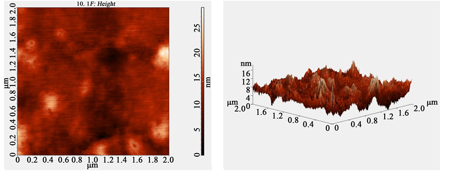 (a) (b)(E)
Figure 10. AFM images of surface after irradiation with laser of intensity of (A) 2 (B) 4 (C) 5 (D) 7 (E) 9 sec.


Figure 11. Surface roughness of the laser treated sample.

Figure 12. Surface roughness versus pulse intensity.
4. Conclusion
Based on the experimental research, a simple theory with the experimental results on the interaction of laser light with surface of high dielectric material has been proposed. This theory actually deals with the temperature dependent oscillation of the atoms and the maximum deflection of the amplitude at which an atom is separated from the lattice, depends upon the laser fluence. The maximum changes in morphology have been observed 430 J/cm2 and also change the spot of the interacted zones. The squared diameter rapidly increases with increase the laser fluence and attains the steady state beyond 350 J/cm2 whereas the size of the spot continuously decrease with an increase in the laser fluence because of a change in times of pulse interaction with rotating sample. Meanwhile the ablation rate from the interaction of the laser light increases with an increase in the laser light due to large changes in temperature from the localized heating of the sample. This shows the maximum impact

Figure 13. Variation of c/a ratio and change in elongation with laser fluence.

Figure 14. Change in dielectric constant and % strain produced in the material with laser fluence.
on change in morphology of the BaTiO3, observed from the SEM and AFM investigation. The roughness of the sample also increases with an increase in the laser fluence. The roughness of the sample has been observed at 430 J/cm2. At the higher laser fluence, the dimple features have been observed in morphology due to the maximum transport of the material from the melted region to the heat flow direction. At the last but not least, the maximum strain has been found in material at the higher laser fluence. This result has been observed from the measurement of dielectric constant at room temperature of the laser treated sample. The other important results are dielectric and the elongated lattice parameter of the laser treated material, which may increase with an increasing strain in the material.
Acknowledgements
The authors are very much thankful to Principal Govt. M. V. M. College and Material Science & Metallurgical Engineering Department MANIT for providing facilities.
Cite this paper
Shivani Saxena,Sanjay Dixit,Sanjay Srivastava, (2016) An Experimental Study of Microstructure through SEM and AFM by Interaction from High Power Femtosecond Laser Wave with BaTiO3. Journal of Modern Physics,07,1068-1081. doi: 10.4236/jmp.2016.710095
References
- 1. Maxwell, J.C. (1865) Philosophical Transactions of the Royal Society of London, 155, 459-512.
http://dx.doi.org/10.1098/rstl.1865.0008 - 2. Heaviside, O. (1950) Electromagnetic Theory. Complete and Unabridged ed. of v.1, 2, 3 with a Critical and Historical Introduction by Ernst Weber. Dover, New York.
- 3. Bloembergen, N. (2000) IEEE Journal of Selected Topics in Quantum Electronics, 6, 876-880.
http://dx.doi.org/10.1109/2944.902137 - 4. Maiman, T.H. (1960) Nature, 187, 493-494.
http://dx.doi.org/10.1038/187493a0 - 5. Rossi, F. and Kuhn, T. (2002) Reviews of Modern Physics, 74, 895-950.
http://dx.doi.org/10.1103/RevModPhys.74.895 - 6. Sundaram, S.K. and Mazur, E. (2002) Nature Materials, 1, 217.
http://dx.doi.org/10.1038/nmat767 - 7. Gordon, J.P. (1983) Optics Letters, 8, 596.
http://dx.doi.org/10.1364/OL.8.000596 - 8. Stegeman, G.I. and Segev, M. (1999) Science, 286, 1518.
http://dx.doi.org/10.1126/science.286.5444.1518 - 9. Schroeder, H. and Chin, S.L. (2002) Optics Communication, 234, 399.
- 10. von der Linde, D., Sokolowski-Tinten, K. and Bialkowski, J. (1997) Applied Surface Science, 109-110, 1-10.
http://dx.doi.org/10.1016/s0169-4332(96)00611-3 - 11. Kirkwood, S.E., Tsui, Y.Y., Fedosejevs, R., Brantov, A.V. and Yu. Bychenkov, V. (2009) Physical Review B, 79, 144120.
http://dx.doi.org/10.1103/PhysRevB.79.144120 - 12. Biciunas, A., Malevich, Y.V. and Krotkus, A. (2011) Electronics Letters, 47, 1186.
http://dx.doi.org/10.1049/el.2011.1925 - 13. Bonse, J., Baudach, S., Krüger, J., Kautek, W. and Lenzner, M. (2002) Applied Physics A, 74, 19-25.
http://dx.doi.org/10.1007/s003390100893