World Journal of Condensed Matter Physics
Vol.4 No.3(2014), Article
ID:48805,16
pages
DOI:10.4236/wjcmp.2014.43016
Microwave Design and Performance of PTB 10 V Circuits for the Programmable Josephson Voltage Standard
Franz Müller, Thomas Scheller, Jinni Lee, Ralf Behr, Luis Palafox, Marco Schubert, Johannes Kohlmann
Physikalisch-Technische Bundesanstalt (PTB), Braunschweig, Germany
Email: franz.mueller@ptb.de
Copyright © 2014 by authors and Scientific Research Publishing Inc.
This work is licensed under the Creative Commons Attribution International License (CC BY).
http://creativecommons.org/licenses/by/4.0/


Received 12 April 2014; revised 3 June 2014; accepted 11 June 2014
ABSTRACT
At Physikalisch-Technische Bundesanstalt (PTB), superconducting 10 V circuits for the programmable Josephson voltage standard (PJVS) are routinely manufactured on the basis of NbxSi1−x barrier junctions. This paper describes in detail the basic design principles for an operating frequency of 70 GHz. It starts with single junctions, discusses their insertion into microstriplines and closes with the whole microwave circuit containing 69,632 NbxSi1−x barrier junctions arranged over 128 microstriplines connected in parallel. The microwave attenuation of this junction type is a key parameter for the 10 V design and we report its experimental determination. Special attention has been devoted to subarrays with just a few Josephson junctions in one of the outermost striplines. The arrangement of these subarrays determines the optimum performance of the complete 10 V series array. The high performance of programmable 10 V circuits fabricated at PTB is characterized by measured operating margins in all subarrays of more than 1 mA centered at the same dc bias current. The observed modulation of the current margins, when changing the frequency around 70 GHz, is explained by microwave reflections caused by the rf waveguide inside the cryoprobe. We determine the current margins in dependence of the output power of a microwave synthesizer and show that 60 mW is sufficient to achieve current margins larger than 1 mA.
Keywords:Josephson Voltage Standard, Programmable Josephson Voltage Standard (PJVS), SNS Josephson Junction, NbxSi1−x Josephson Junction

1. Introduction
Nowadays programmable Josephson voltage standards (PJVS) [1] with output voltages up to 10 V replace more and more conventional 10 V Josephson voltage standard (JVS) systems operated between 70 and 75 GHz [2] . PJVSs are based on series arrays of overdamped Josephson junctions (JJs) divided into smaller independently biased subarrays. The overdamped Josephson junctions are externally or intrinsically shunted and exhibit a current-voltage characteristic (IVC) with a negligible hysteresis. In contrast to underdamped and therefore hysteretic SIS (S = superconductor, I = insulator) junctions used for conventional JVS systems, overdamped Josephson junctions display single-valued Shapiro steps under microwave irradiation. Each of these constant voltage steps, including , can be attributed to a definite dc bias current. This special property opens up new areas of application beyond simple dc metrology covered by the conventional JVS. Today, the PJVS constitutes, together with the Josephson arbitrary waveform synthesizer (JAWS) based on pulse-driven Josephson junctions [3] , the basis of modern ac voltage metrology. PJVS circuits representing the current state of technology are using NbxSi1‒x barrier junctions. This junction type allows operating frequencies from 15 to 70 GHz by changing the Nb content [4] . For this reason, it complies perfectly with the strategy of PTB to retain an operating frequency of 70 GHz, or, in other words, to continue to use the microwave equipment in operation for the conventional JVS at most National Metrology Institutes (NMI).
Section 2 of this paper describes the search for a suitable Josephson junction type and for a normal-conducting barrier material (N) in SNS (S = superconductor) junctions that are required for a 70 GHz design. Thereafter, the basic design principles starting from single junctions, their integration into microstriplines and completion of the whole microwave circuit for 70 GHz will be discussed. Section 3 concentrates on experimental results obtained for different design variants regarding the arrangement of the smallest subarrays. The performance of programmable 10 V circuits fabricated at PTB is characterized by the measured current margins for all relevant array segments. Furthermore, we present measured current margins in dependence of the frequency in a small band around 70 GHz and discuss the requirements for the microwave power and their impact on the use of cryocoolers. A summary and some conclusions are given in section 4. With this paper, the authors intend to provide an overview of the properties of 10 V PJVS circuits made by PTB and a useful guideline for their use. The main metrological applications of the 10 V circuits fabricated at PTB have been described in detail in a review paper by Behr et al. [5] .
2. 70 GHz Design of 10 V Circuits for the PJVS
2.1. Development of Robust Josephson Junctions Suitable for 70 GHz Operation
To ensure optimum operation of a Josephson voltage standard, the product of critical current Ic and normal resistance: :
: (characteristic voltage) of the used Josephson junctions has to be matched to the microwave frequency, i.e. it should be Vc ≈ 145 µV for 70 GHz (cf. 2.2.) [6] .
While the proof-of-concept experiment [1] was still executed with externally shunted SIS junctions operated at 70 GHz, shortly thereafter the National Institute for Standards and Technology (NIST) favoured intrinsically shunted SNS junctions enabling larger Shapiro steps, i.e. a better adjustability of the operating point and larger noise immunity [7] . Due to the relatively low resistivity of the normal-conducting barrier materials commonly used and available at that time, e.g. AuPd, HfTi, or later on, TiNx, microwave design and operating frequency were fixed to the range from 15 to 20 GHz and were maintained in later developments with other barrier materials. In contrast, PTB searched from the beginning for a junction technology which would allow retaining the operating frequency of 70 GHz used for conventional JVSs. A 70 GHz drive reduces the number of junctions necessary to reach a certain voltage level by a factor of 4 to 5, i.e. 70,000 JJs instead of 320,000 JJs for 10 V. The entire microwave distribution network for 70 GHz can be completely fabricated on chip. In this way, the requirements for fabrication technology and microwave design are more relaxed.
Motivated by the reliable Nb-Al technology successfully established throughout the 1990s for the fabrication of conventional 10 V SIS JVSs at PTB [8] [9] , the intrinsically shunted SINIS Josephson junctions (S = Nb, I = AlOx, N = Al) composed of two very transparent AlOx barriers quickly moved into the focus of the PTB researchers. The double-barrier structure of this junction type can be easily tuned to 70 GHz. As early as in 2000, PTB reported first programmable 10 V PJVS circuits with SINIS junctions for 70 GHz drive [10] . However, their limited resolution due to six subarrays and a step width of 200 µA restricted their applications to fast and simplified dc voltage calibrations. Continuous progress in fabrication technology and several design optimization steps led six years later to the first-ever 10 V PJVS circuit really suitable for ac applications [11] . These 10 V circuits with 69,632 series-connected SINIS JJs offered a high resolution and sufficient noise immunity because they were divided into 16 subarrays and the step width of all array segments was larger than 0.6 mA. However, wide adoption in ac metrology suffered from the low fabrication yield, because a few of the very thin insulating AlOx barriers  of the SINIS junctions were obviously damaged by plasma-induced charging effects occurring during several fabrication steps (dry etching) of the microwave circuits [12] .
It is well known that SNS junctions with normal-conducting (N) barriers, which are usually relatively thick (d > 10 nm), are very robust and free of these yield problems connected to very thin insulating layers with pinholes. For this reason, PTB was continuously and simultaneously to its SINIS activities, seeking a SNS junction type that can be simply implemented as a drop-in replacement in existing 70 GHz SINIS designs of PJVS circuits. Finally, amorphous NbxSi1−x, “rediscovered” by the NIST [4] , was the appropriate SNS-like normal-conducting material. The resistivity of NbxSi1−x, already known as a candidate for JJs since 1987 [13] , can be tuned by its Nb content from insulating to metallic and represents an ideal N-barrier for SNS junctions. NIST first used this material for PJVS circuits driven around 15 GHz. In close cooperation between PTB (design, circuit fabrication) and NIST (trilayer deposition) the first 10 V PJVS circuits with 69,632 NbxSi1−x barrier junctions operable at 70 GHz were realized in 2008 [12] . Two years later, NIST reported their first own 10 V arrays with about 300,000 triple-stacked junctions and the same barrier material, tuned however for operating frequencies from 16 to 20 GHz [14] . Another type of a 10 V PJVS circuit with double-stacked NbN-TiNx-NbN junctions operated at 16 GHz and 10 K was developed by the Japanese National Institute of Advanced Industrial Science and Technology (AIST) [15] .
After the purchase of a special sputtering cluster tool allowing the automated deposition of the barrier by co-sputtering of Nb and Si in a separate chamber, PTB has been fabricating 10 V circuits with NbxSi1−x barrier junctions routinely and completely in-house since 2010. Details of this fabrication process are described elsewhere [12] [16] . Using this technology and benefiting from the advantages of the 70 GHz design mentioned above, we also fabricated the first-ever 20 V array for PJVSs simply by using 69,632 double stacked JJs instead of the single junctions in the 10 V design [17] .
The NbSi technology has significantly improved the yield of PJVS circuits. For the first time, 10 V circuits with no defects, i.e. no “missing (shorted) junctions”, as compared to 10 V SINIS arrays [11] , could be manufactured in a complex fabrication process. 10 V arrays with NbxSi1−x barrier junctions show a much better performance than those with SINIS junctions. A current width of about 1 mA for the 1st Shapiro steps of all subarrays is typical for the 10 V circuits fabricated at PTB (cf. 3.2.).
2.2. Single Josephson Junctions with NbxSi1−x Barriers Optimized for 70 GHz
The underlying physics of Nb-NbxSi1−x-Nb Josephson junctions has been thoroughly investigated by Scheller [18] . Major properties of the semiconducting NbxSi1−x tunneling barrier for different doping levels of Nb, its influence on the  -noise and on the specific capacitance have been summarized by Müller et al. [17] . By controlling the Nb content “x” and the thickness “d” of the NbxSi1−x barrier, it is possible to realize two limiting cases representing different junction types: 1) An SIS-like junction with a nearly maximum hysteresis in the IVC for
  (pure semiconductor) and
 , or on the other hand, 2) an SNS-like junction with no hysteresis in the IVC for
  (fully degenerate semiconductor) and
 . Junctions designed for an operating frequency of 70 GHz occupy a position between these limiting cases: They present a small (almost negligible) hysteresis and are strictly speaking neither SIS nor SNS junctions. In the following they are called NbxSi1−x barrier junctions. Their barrier is typically characterized by
 ,
,  and a specific capacitance of about 380 fF/µm2. This barrier composition enables a characteristic voltage of
  (with
(with  determined at
 ). Such a value for Vc is optimal for an operating frequency
  as the normalized frequency
  [6] . Under this condition, Vc may also be derived from the second Josephson equation describing the ac Josephson effect (cf. e.g. [19] ):
 (1)
(1)
setting the integer  and
and  (
( elementary charge,
  Planck’s constant). On the other hand, it can be deduced from Equation (1) that a single Josephson junction under microwave irradiation of 70 GHz generates constant voltage steps corresponding to multiples of ±145 µV. Typically, PJVSs only use Shapiro steps of 1st (±145 µV) and 0th (0 V) order [1] . The current width, in the following also called current margin, of the 1st Shapiro step reaches a theoretical maximum when the
  product is adjusted to 145 µV. As current density jc and resistivity of a junction are up to a certain degree independently adjustable by the co-sputtering of Nb and Si, it is possible to obtain the desired
  for a given (designed) junction area A. To select reasonable values of
  and A, it should be taken into consideration that the value of the critical current
  determines the necessary rf power (together with the stripline impedance). Based on our experience with SINIS designs [12]
where a maximum critical current of 3 mA was reasonable, we set  for the present 10 V design with NbxSi1−x barrier junctions. The width “w” of the junction, perpendicular to the extension of the array, is an important parameter for the microwave impedance of the microstripline. For the present 10 V design a value of
  was chosen. The length “l” of the junction, which should be “short” to limit the length of the array, was fixed to
 . For these geometrical design parameters resulting in
  of a single junction, it is possible to adjust current density and critical voltage to about
  and
and , thus enabling optimum formation of Shapiro steps.
2.3. 70 GHz Design of Microstriplines with Embedded NbxSi1−x Barrier Junctions
A simple approach to increase the voltage from 145 µV up to 10 V is the series connection of many junctions. In order to ensure that the “quantized” voltages U1 of each junction add to a much larger quantized voltage level, the series-connected JJs should have nearly the same shape of the IVC under microwave irradiation, i.e. Shapiro steps with the same current width and positioned at the same place of the IVC. This requires that nearly the same microwave current is injected into each junction, apart from a small scattering of the junction parameters. Therefore, microwave designs for series arrays used in all types of JVSs had to ensure a nearly homogeneous distribution of the rf power along the array. Superconducting microstriplines with embedded Josephson junction arrays can provide the required homogeneity [20] and were therefore used as a basic design element in most conventional 10 V JVS circuits with hysteretic (underdamped) SIS junctions driven at 70 GHz and above. The insertion of nonhysteretic (overdamped) junctions in superconducting striplines was therefore the first logical step in creating a 70 GHz design for a PJVS. However, a new and surprising effect was detected in this case [21] : In contrast to highly-hysteretic SIS junctions, arrays of embedded nonhysteretic junctions (SINIS, SNS) show self-oscillation coupling effects if their dc bias exceeds the critical current. These coupling effects [12] [22] occur in “active” striplines with , and partly compensate the relatively large microwave attenuation expected for the series connection of many JJs. The attenuation can be estimated according to Kautz for “passive”
striplines , a model that was originally successfully developed for embedded SIS junctions with so-called “zero-current” Shapiro steps
  [23] . The maximum number of Josephson junctions that can be inserted in a single microstripline is the key parameter of the microwave design. For this reason, we determined experimentally the microwave attenuation for a stripline with embedded NbxSi1−x barrier junctions. The scheme of the setup used in the measurements is shown in Figure 1. The setup allows varying the microwave power supplied by means of an adjustable attenuator at the top of the cryoprobe. First we measure the step width of IVCout with no external attenuation
 . The attenuation of 1500 JJs is given by D when IVCin matches the previous IVCout. In the “passive” case
  the measured attenuation per junction is about 0.022 dB (theoretically: 0.04 dB). Coupling effects occur in “active” striplines
  and reduce this value to 0.009 dB/JJ.
The deviation between experimental and theoretical value for the passive case is possibly due to the influence of the Si substrate on the microwave propagation. As a result, the microwave design has to take into consideration that short but inactive  array segments can present a higher attenuation than longer and active subarrays. On the other hand, experience previously collected with SIS arrays for conventional JVSs [8] suggest that the maximum microwave attenuation should not exceed 5 dB to ensure a sufficiently homogeneous distribution of the rf power. As a result, the maximum number of NbxSi1−x barrier junctions in a single and actively driven stripline should be about 550. This number corresponds to an earlier result found for SINIS arrays that up to 500 junctions the maximum current width of the 1st Shapiro step is only slightly reduced (to 80% of Ic) [24] . The present microwave design is realized on basis of the so-called inverted microstripline structure (Figure 2), which was already successfully used for SIS and afterwards for SINIS circuits [25] . In this design, the superconducting ground plane is placed on top instead of underneath the array. Later on (cf. 2.4.), it will become apparent, that such an inverted microstripline substantially simplifies the microwave design for the whole circuit.
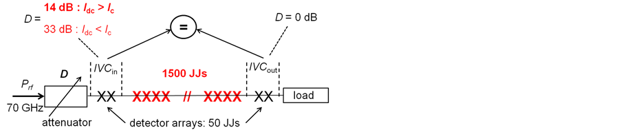
Figure 1. Schematic setup for microwave attenuation measurements.
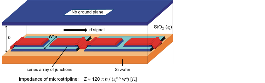
Figure 2. Scheme of an inverted stripline structure with embedded JJs.
Moreover, it allows the direct deposition of the junction trilayer on a clean and polished wafer surface. It is known that a rough surface, due to a previous etching process or the deposition of a thick dielectric film, degrades the quality of the trilayer, especially the sharpness of its interfaces. Last but not least, a Nb ground plane on top of the circuit protects the junction array very well. The microwave impedance “Z” of a single stripline (Figure 2) is an important design parameter that determines the necessary rf power to generate Shapiro steps of optimum size. For the design values: ,
, 
 and
and  for SiO2 [26] , the characteristic impedance of an “undisturbed” microstripline (neglecting the influence of the substrate and without junctions) becomes approximately
 . Knowledge of this impedance allows a rough estimation of the rf power P that should be at least coupled into each “stripline-array”, according to
  with
with  (i: rf current) [27] . For
 , a single microstripline requires approximately
 .
.
2.4. 10 V Circuit Design with 69,632 NbxSi1−x Barrier Junctions
The second generation of programmable 10 V circuits developed and fabricated at PTB [11] is subdivided into 16 array segments whose junction numbers follow an almost binary sequence. The sequence is exactly binary at the beginning,  (m: 0, 1, 2, 3) giving the numbers 1, 2, 4, and 8. The next segment with 17 junctions breaks this series and starts a new “binary” sequence according to
  (p: 0, 1, ×××), resulting in: 17, 34, 68, 136, 272, and so on. To approach the 10 V level as close as possible, we need a largest subarray with 34,816 junctions
 , leading to a total of 69,630 junctions in the array. The fundamental Josephson equation specially formulated for the programmable version of the Josephson voltage standard becomes:
 (2)
(2)
with , or ±1 and
  (Josephson constant). For
  and
and , Equation (2) delivers a maximum voltage amplitude of ±10.0788 V which is very close to the 10 V level. To realize for special measurement purposes two equal halves of the circuit (each with 34,816 junctions), two extra single junctions have been added. Therefore, the total number of junctions amounts to 69,632.
For the robust operation of rapidly programmable circuits with a “time-variant” number of junctions , the current margins of each voltage step
  generated by the activated array segments should exceed a certain minimum. From our experience and also supported by other researchers [28] , a value of at least 0.8 mA is desirable. The current width of a Shapiro step of order n:
  generated by each junction (embedded in a stripline) under microwave injection is proportional to the critical current
  and varies with the rf current
  [27] according to the total amount of a Bessel function
 :
:
 (3)
(3)
All 69,632 JJs of the 10 V design have to be distributed over microstriplines rf-driven in parallel, taking into account the following restrictions:
• A binary number  of parallel-connected striplines should be used for geometrical reasons and for equal distribution of the rf power coupled by the antenna (Figure 3). In order to keep the necessary rf power for the whole circuit low, N should be as small as possible.
• As the maximum number of junctions in one stripline is evaluated to be about 550 (cf. 2.3.), we concluded to use 128 (27) striplines.
• To minimize their microwave attenuation, large “array-striplines” should always be biased collectively to benefit from the previously described self-oscillation effect.
• Only small segments should be used unbiased  if placed in front of active subarrays. Due to the attenuation when unbiased, “large” subarrays must be placed after smaller segments, relative to the microwave propagation.
• The active circuit area comprising all junctions should be concentrated as much as possible to minimize the parameter spread, which also means a minimum lateral distance between the striplines.
• With the exception of the two outermost striplines, superconducting dc connections can only be made to the ends of the striplines.
• To realize at the same time a series connection of all junctions and a parallel rf power supply for each stripline, dc blocks have to be inserted at the output of the rf-distributing network (microwave splitters).
The 10 V microwave design schematically depicted in Figure 3 is the result of these conditions. One 10 V chip covers an area of 24 mm × 10 mm. A finline antenna [29], built by the Nb ground plane and the Nb base metallization of the trilayer, captures microwave power from a rectangular waveguide. The rf power is divided by microwave splitters and fed over capacitors (dc blocks) into the array-striplines connected in parallel. All microstriplines are extended by homogenous Nb strips beyond the array length in order to reach the microwave termination and to match all lengths. The microwave termination of each array stripline is necessary to avoid an inhomogeneous rf power distribution by standing waves. The use of a AuPd load as part of the circuit ground is a special feature of the PTB design. This resistive ground plane, together with the Nb strips which lie underneath and which are connected to the ends of the junction arrays, forms the continuation of the inverted microstripline structure. It seems to be the only reasonable design variant that enables the necessary superconducting connection between the arrays and the 23 bonding pads arranged at the right part of the circuit. The alternative design variant, using AuPd strips and a superconducting ground plane extending over the whole circuit, would make it nearly impossible to establish superconducting connections between dc pads and all array segments.
The distribution of the 69,632 NbxSi1−x barrier junctions over the 128 microstriplines is detailed in Table1 From the “low potential dc pad”, connected to the end of the 1st row (Figure 3), the smallest array segments are originally arranged in decreasing (regular) order of junctions (68, 34, 17, 8, 4, 2, 1, 1, 1), before beginning with the 2nd row, the “natural” quasi-binary sequence is continued: 136, 272, 544, etc. For comparative studies, a small number of chips with a reversed order of the smallest segments in the 1st stripline have also been fabricated. Unbiased junctions in front of active array segments only occur in the 1st row of the 128 striplines, i.e. in an extreme case (reversed order) 135 passive junctions lie in front of one active Josephson junction.
3. Experimental Investigations on 10 V PJVS Circuits with NbxSi1−x Barrier Junctions
3.1. Measuring Setup and Instructions for Use
The 10 V chips (Figure 4) are glued on special carriers and electrically connected by wire bonding. For an optimum microwave coupling the antenna is inserted to 70% of its length in the slot of a WR12 waveguide. The use of a commercially available microwave synthesizer for frequencies around 70 GHz with a maximum output power of about 160 mW simplifies substantially the operation of the programmable circuit. This computer-controlled synthesizer only requires a 10 MHz reference signal without the need of a phase lock loop. To
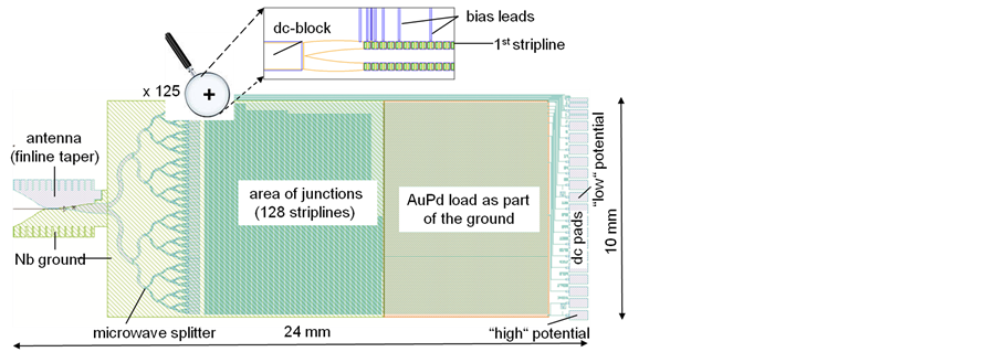
Figure 3. Microwave design of a programmable 10 V circuit operated at 70 GHz. The magnification shows the 1st stripline with the smallest segments arranged in “regular” order.
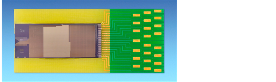
Figure 4. Photograph of a 10 V PJVS circuit for operation at 70 GHz mounted on a special chip carrier.

Table 1. Distribution of 69,632 Josephson junctions over 128 parallel-connected striplines in a programmable 10 V circuit with 16 subarrays.
realize fast programmability, e.g. for the stepwise synthesis of an ac signal of low frequency (<2 kHz) [5] , each of the 16 segments of the binary-divided 10 V array can be separately driven by its own rapidly switchable bias source. However, the IVCs presented in this paper have been recorded in most cases by using only one computercontrolled current source (resolution: 20 µA) and a digital voltmeter.
Immediately after cooling down the array and before starting the operation, it is advised to check whether the circuit is free of magnetic flux. For this purpose, the IVC of the whole circuit without microwave injection should be visualized with high resolution using an oscilloscope. In case of trapped flux, one or more junctions display reduced critical currents. If there is a heater integrated in the cryoprobe, the array can be conveniently warmed up to remove the flux [30] . Otherwise one has to lift up the cryoprobe before slowly lowering it again (cooling down). Unfortunately, it is possible that even after repeated warming up and cooling down the flux remains trapped. This case occurs most likely after a quick warming up so that the circuit is covered by a lot of condensed water. Tiny magnetic particles from the surrounding magnetic shield or from other parts (screws) used for fixing the cryoprobe are possibly transported by the condensing atmosphere and/or flowing He gas. It is therefore advantageous to cover the inner surface of the cylindrical shield with a plastic material and to avoid screws made from alloys containing ferromagnetic components. To remove magnetic contaminants from the surface of the circuit, it is advised to do this with large precaution in a clean room under microscopic observation.
3.2. Current Margins and Effect of Parasitic Microwaves for Different Arrangements of the Smallest Subarrays
The 70 GHz design with a nonuniform distribution of the junctions over the 128 parallel-connected striplines (Table 1) represents a trade-off between homogeneous microwave supply and geometrical constraints for the “binary” array segments. Each segment with more than 68 JJs occupies entirely one or more striplines, which are therefore always “active” when the considered segment is biased on the first-order Shapiro step . In contrast, the smallest subarrays (1, 1, 1, 2, 4, ×××, 68) are all embedded in the first (outermost) stripline. In this case, the microwave propagation along the stripline can be affected by inactive array segments. Our observations indicate that the bias leads connecting the smallest subarrays can couple parasitic microwaves from the outside. The magnetic shield surrounding the cryoprobe sample space contains parasitic microwave radiation because the transition from the waveguide to the circuit antenna is not at all ideal and a certain amount of rf power leaks from the waveguide into the silicon wafer [26] and to the cavity of the cylindrical cryoperm shield. Parasitic microwave power injected in such a way can be superimposed on the “regularly” propagating microwave inside the stripline.
For a rough evaluation of possible effects on the behavior of the circuits, we compare the number of “excellent” 10 V circuits with different designs A, B and C for the 1st stripline and D with a special ground plane. The investigated circuits come from 8 wafers which were processed within a period of two and a half years. Each wafer contained two chips of each of the designs A, B, C and D. Those 10 V circuits corresponding to the so-called “1 mA criterion” will be referred to as “excellent”, as they show a 10 V Shapiro step (all array segments activated) of 1 mA or larger under microwave irradiation. Figure 5 displays, for an example, the IVC of an excellent 10 V circuit with design A. Table 2 lists the features of the used designs A, B, C and D. There are different arrangements of the smallest subarrays: “regular” (1, 1, 1, 2, ×××, 68) or “reversed” (68, 34, ×××, 1, 1, 1), each relative to the feeding point of the rf power (stripline input). Additionally, one can distinguish between a direct connection of the subarrays containing 1, 1, 1, 2 and 4 junctions and a connection over inserted sections of a homogeneous microstripline. The latter design modification was made to investigate whether very close bias leads (cf. Figure 3) couple parasitic microwaves in a different manner than more distant bias leads. We also tested chips with slots in the ground plane between the striplines (design D) aiming to reduce the flux trapping. A comparison of the numbers of excellent 10 V circuits resulting from each design variant (Table 2) suggests that the rather small modifications made are not really relevant for the behavior of the entire circuit. At this point it should be mentioned that characterization and classification of the fabricated 10 V circuits in “excellent” and “good to very good” ( to 1 mA) has been accomplished in most cases by measuring only the whole circuit, i.e. with all subarrays activated by one current source. Only in a few cases the large segments including the entire 1st stripline
  have been measured too. For that reason, one of the motivations for this paper was also a more thorough investigation of the smallest subarrays
  and to demonstrate how
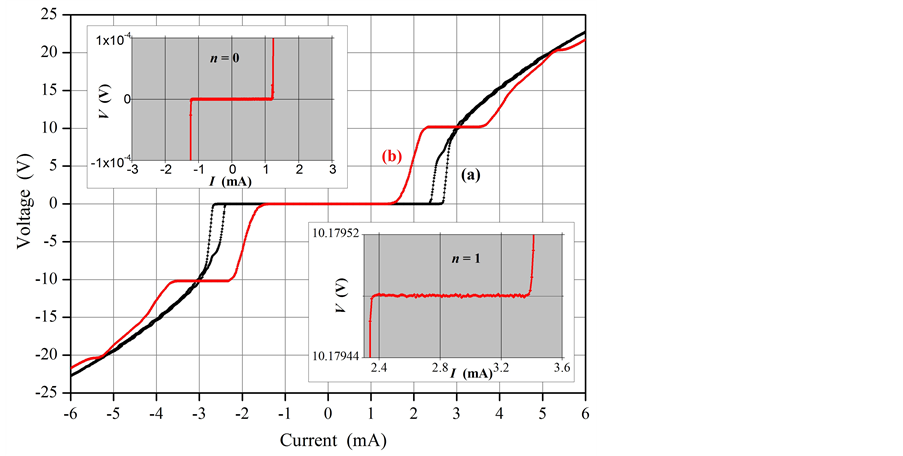
Figure 5. IVC of a 10 V PJVS circuit classified as “excellent” with 69,632 NbxSi1−x barrier junctions. (a) without microwaves, (b) with microwaves at 70.7 GHz and approximately 60 mW at the antenna. The insets show the 10 V step  and the zero-voltage step
  with high resolution. Junction parameters:
 ;
; .
.
Table 2. Design variants of 10 V circuits and the number of excellent 10 V circuits fabricated within two and a half years (for explanation see text).
their microwave properties depend on the design of the 1st stripline.
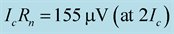
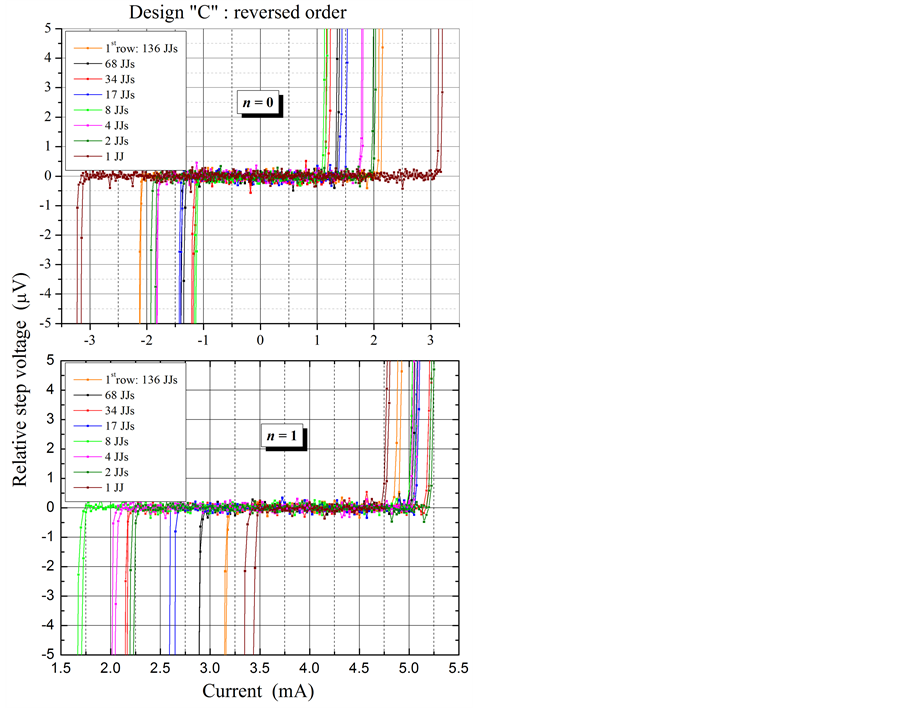
The practical use of programmable voltage standards, especially if fast switchable dc bias sources are used, requires that both the 0th and the 1st constant voltage step of each array segment should be large enough to ensure a good adjustability of the dc operating point and sufficient noise immunity. As a result, the zero-order Shapiro step has to be considered too, especially for the smallest subarrays in the 1st stripline. As explained in 2.4, the subarrays closer to the microwave feeding point have the smaller number of junctions (except of design C) and can be easily overdriven. Figure 6, representative for the designs B and C, shows the current widths of the Shapiro steps with  and +1 for all array segments in the 1st stripline.
For better comparability and considering thermal voltages, the microwave-induced steps of constant voltage are described by their relative voltage as a function of the dc bias current. Figure 6 illustrates that the current widths of the steps corresponding to  scatter more for 10 V circuits of design C. This observation demonstrates a better homogeneity of the microwave power along the 1st junction stripline in the case of a regular order (design B) of the smallest array segments. Figure 6(a) displays, furthermore, that the array segment
  with
with , lying at the end of the stripline and after 68 unbiased junctions, has a minimum step width of
  or in relative units of
 . Design C (Figure 6(b)) in contrast, enables “only” a step width of 1.3 mA
  for the single junction
  at the end of the 1st stripline. Despite these differences, both designs fulfill, in principle, the 1 mA criterion for the smallest segments, i.e. they are
 (a)
(a) (b)
(b)
Figure 6. Current widths of the Shapiro steps  and
and  of the smallest array segments
  to
to . (a) 10 V PJVS circuit with design B. Junction parameters:
 ;
; ; (b) 10 V PJVS circuit with design C. Junction parameters:
well suited for ac applications. However, the 1 mA criterion is difficult to meet for the 0th step in some cases, when the critical current is “small” . Such a situation can arise if parasitic microwave is coupled into the 1st stripline or if the load is incorrectly matched. In both cases the rf power distribution becomes inhomogeneous and may lead to reduced 0th steps (below 1 mA) in one or more segments without significant changes to the 1st step. Figure 7 shows the Bessel functions of 0th and 1st order
  in dependence on the microwave current
  and explains this effect: In a certain range of the microwave power P
(hatched region) the 0th step  is quickly reduced, whereas the width of the 1st Shapiro step
  remains nearly unchanged.
In most cases, a slight change of the array position relative to the surrounding magnetic shield can lead to a significant change in the 0th step, so that  can be achieved for all subarrays in the 1st stripline. This behavior is most pronounced for circuits with design D. The comparative evaluation of 5 wafers with critical currents smaller than 5 mA delivers significantly smaller values for
  while forming a 10 V step for circuits with the designs A and D. This is in our opinion due to a larger amount of parasitic microwave coupled into the 1st stripline from outside over the bias leads (Figure 3) and possibly favored by slots in the ground plane (design D). The aim to reduce the flux trapping (cf. 3.1.) by means of a ground plane with slots between the striplines has not been realized.
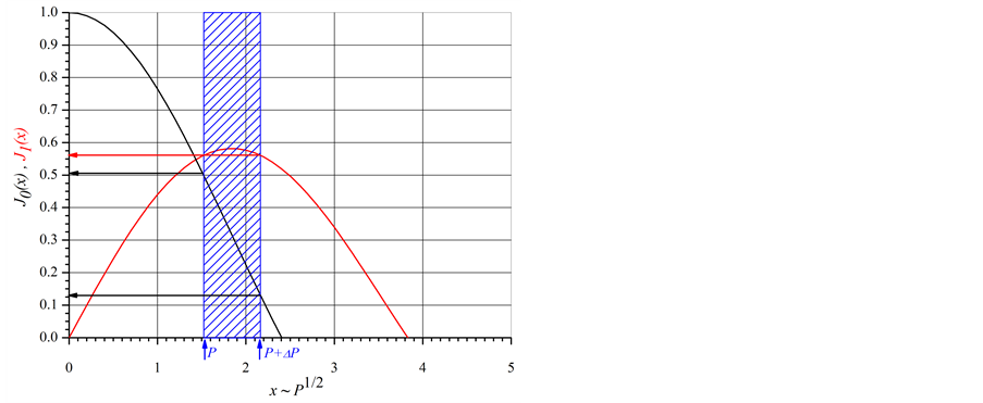
Figure 7. Plot of the Bessel functions of the 1st kind:  and
and . The argument of the functions is proportional to the injected microwave current
 . The hatched region and arrow lines illustrate the drastic change in the 0th step widths for a change in microwave power
  which leaves the width of the 1st step unchanged.
In summary, one can conclude from these investigations that the design variants A and B with a regular order of the smallest subarrays are obviously most suitable for the operation of a programmable voltage standard, in which design B, having enough space between all lateral dc bias leads, is less sensitive to coupling of parasitic microwave.
An outstanding feature of excellent 10 V circuits fabricated at PTB is that both small and large array segments can be operated on the 1st Shapiro step with the same dc bias current. This is a surprising property considering the unequal distribution of nearly 70,000 junctions over the 128 striplines connected in parallel. Figure 8(a) demonstrates for a bias current of 6 mA that the current margins at each of the 16 voltage levels are at least 1 mA. In addition, we have also checked, for reasons explained previously, the current width  of the zero-order steps for the same power level. Figure 8(b) displays these steps for the smallest segments from
  to
to  (regularly arranged). An investigation of the larger subarrays (
 to
to ) with regard to
  is unnecessary because their microwave-induced reduction of the critical current is comparatively small, which results without exception in large values
 .
.
Whereas Figure 8 is typical for 10 V circuits with relatively large critical currents (compared to the design value of 5 mA), analogous microwave behavior could already be demonstrated earlier for circuits with an  of about 3 mA [5] . The fact that circuits with low
  have similarly good properties
  as those with a “large” one
  is a second outstanding feature of our 10 V samples.
The thermal load generated by these circuits in operation at 10 V is therefore lower than 100 mW. This value has to be compared with the values reported in the literature for other designs of 10 V PJVSs: 350 mW at 4.2 K [31] or about 470 mW at 10 K [15] .
3.3. Performance of Programmable 10 V Circuits with NbxSi1−x Barrier Junctions in a Narrow Band Close to 70 GHz
Since the used microwave source (cf. 3.1.) delivers the largest amount of microwave power in a frequency range from 70 to 70.7 GHz, we restricted our investigations to this frequency band. Exact statements regarding the broadband properties of our circuits with NbxSi1−x barrier junctions are therefore not possible. However, from earlier investigations of 10 V SINIS circuits with basically the same microwave design except for the geometry and current density of the junctions, we assume that 10 V circuits with NbxSi1−x barrier junctions should work as well at 75 GHz, but would require more microwave power [11] . In any case, it should be noted that for optimal operation of the PJVS circuit the critical voltage of the junctions has to be adjusted according to  close to the selected operating frequency. In principle, it is difficult to decide whether the design of the circuit, including mismatches, or the design of the single junction (electrical parameters:
 ) is the reason for a special frequency behavior. The microwave response of 10 V circuits shows a lot of resonances
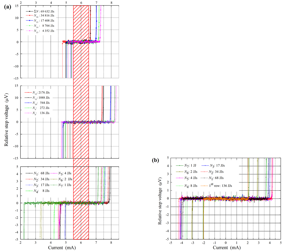
Figure 8. Current widths of all relevant Shapiro steps of a 10 V PJVS circuit (design A). Junction parameters: ;
;  at
at . (a)
. (a)  for all array segments
  to
to . The hatched region illustrates a current margin of 1 mA for all array segments biased at 6 mA; (b)
  for the array segments
  to
to  in the 1st stripline.
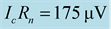
if the frequency of the synthesizer is changed by small steps from 69.6 and 70.9 GHz. Figure 9 depicts the current margins corresponding to 0 V  and to 10 V
  for two different rf power levels if all subarrays are activated by a single current source. The dashed line marks the region above which robust operation as a rapidly programmable voltage standard is possible. It can be seen that there are numerous frequencies where excellent operating conditions are fulfilled, i.e. where the 1 mA criterion holds. Obviously there is a regular modulation of the current margins best visible in Figure 9(a). We found an explanation for this phenomenon by investigating the measuring probe by means of a network analyzer. If the waveguide at the cold end of the measuring probe used to immerse the sample holder into a liquid helium dewar was shorted, resonances with a period of about 100 MHz could be observed in reflection. This period is clearly visible in Figure 9(a) and is correlated to the length of the waveguide used for the measuring probe. The waveguide is approximately 1.25 m long and there are two reflections for the microwave, first at the WR12 waveguide input flange with a thin foil of PTFE to prevent helium gas losses, and second at the end of the WR12 waveguide in the cold part. Multiples of the half wavelength match in this length and cause the frequency modulation of the current margins.
Figure 10 compares the frequency behavior of the two halves of a 10 V circuit. The largest array segment
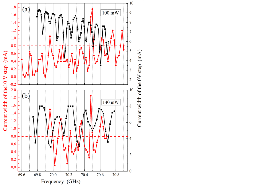
Figure 9. Current width of the 10 V and 0 V steps as a function of the frequency (in a small band at approximately 70 GHz) for two different output power levels of a microwave synthesizer: (a) = 100 mW and (b) = 140 mW. Junction parameters: ;
; .
.
Figure 10. Current width of the 5 V steps generated by the two halves of a programmable 10 V circuit as function of the frequency in a small band at approximately 70 GHz. Junction parameters: ;
; .
.
 (34,816 JJs) with an almost homogeneous distribution of the junctions over the striplines #69 to #128 (Table 1) displays at nearly all frequencies for the 5 V step
  larger current margins than the other half of the circuit (sum of segments
  to
to ) which is characterized by an inhomogeneous distribution of the junctions over the striplines #1 to #68. Nevertheless for some frequencies just below 70 GHz, the current margins of both halves are in principle identical. For such a frequency, the current margins at 5 V
  and at 0 V
  have been determined as a function of the rf power (synthesizer output) in case the whole circuit is driven by a single current source. Figure 11 demonstrates that 10 V circuits, even with a relatively large critical current, can be driven by a microwave power of about 60 mW, provided a suitable frequency has been selected. Therefore commercial Gunn diodes with a maximum output power of 80 to100 mW can be used in principle too. However, it seems more difficult to look for a suitable frequency with a Gunn diode than with a computer-controlled microwave synthesizer.
4. Summary and Conclusion
This paper presents the state of the art for 10 V programmable Josephson voltage standards (PJVS) at PTB. The technological progress from the appearance of the fundamental idea in 1995 to the current state of technology, characterized by the use of NbxSi1−x barrier junctions, is described. The barrier of this special kind of Josephson junctions can be tuned for a wide range of driving frequencies. The operation of the arrays in the same microwave frequency range that has already been used for conventional JVSs, around 70 GHz, strikes us as the most obvious and promising way for PJVSs. We therefore decided on this frequency range very early even before the reappearance of Josephson junctions with NbxSi1−x barriers. The paper underlines the advantages of a 70 GHz drive and discusses step by step the creation of a 10 V design based on striplines with embedded NbxSi1−x barrier junctions connected in parallel for the microwaves.
Different designs for the arrangement of the junctions in the outermost stripline and the nature of the ground (cover) plane have been experimentally compared by evaluating the current margins for the steps  and
and . In addition, the susceptibility to flux trapping and to coupling of parasitic microwaves has been investigated. Optimum 10 V circuits for PJVSs have homogeneous (gapless) ground planes and a regular order of the smallest array segments with enough space between them (design B). It is shown that a complete and safe classification of the circuit performance is only possible by evaluating the current margins for the steps of order
  and
and  of all array segments in the 1st stripline.
We show that the PTB circuits classified as “excellent” can be operated with the same dc bias current in all array segments while keeping the current margins larger than 1 mA. The resonances in the current margins of the PJVS circuits observed in a small frequency band around 70 GHz have been related to the length of the waveguide used in the measuring probe. In addition, 10 V circuits with small critical currents  present low thermal loads (<100 mW), due to the combined dc and rf power, and are therefore very advantageous for operation in cryocoolers. Even though a powerful compact microwave synthesizer was used for the experiments described in this paper, the results obtained indicate that also Gunn diodes with an output power of about 100 mW can be used for the routine operation of 10 V PJVSs.
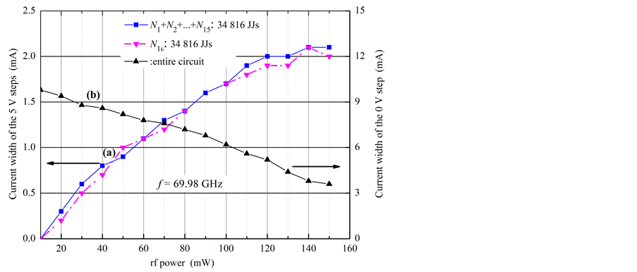
Figure 11. Current width of the 5 V  and 0 V
  steps generated by the two halves of a programmable 10 V circuit as a function of the output power of a microwave synthesizer operated at 69.98 GHz (cf. Figure 10). Junction parameters:
 ;
; . (a) current widths of the two 5 V steps; (b) current width of the 0 V step of the entire circuit.
The results clearly demonstrate that the fabrication process of arrays with NbxSi1−x barrier junctions has achieved the major technological requirements to be robust, reliable, and reproducible. State of the art 10 V circuits are available for routine use in PJVSs that successfully extend the application of Josephson voltage standards more and more from dc to ac.
Acknowledgements
The authors would like to thank R. Wendisch, T. Weimann, B. Egeling, P. Hinze, K. Störr and P. Duda for technical support, and O. Kieler for helpful discussions.
References
- Hamilton, C.A., Burroughs, C.J. and Kautz, R.L. (1995) Josephson D/A Converter with Fundamental Accuracy. IEEE Transactions on Instrumentation and Measurement, 44, 223-225. http://dx.doi.org/10.1109/19.377816
- Popel, R. (1992) The Josephson Effect and Voltage Standards. Metrologia, 29, 153-174.http://dx.doi.org/10.1088/0026-1394/29/2/005
- Benz, S.P. and Hamilton, C.A. (1996) A Pulse-Driven Programmable Josephson Voltage Standard. Applied Physics Letters, 68, 3171-3173. http://dx.doi.org/10.1063/1.115814
- Baek, B., Dresselhaus, P.D. and Benz, S.P. (2006) Co-Sputtered Amorphous NbxSi1-x Barriers for Josephson-Junction Circuits. IEEE Transactions on Applied Superconductivity, 16, 1966-1970.http://dx.doi.org/10.1109/TASC.2006.881816
- Behr, R., Kieler, O., Kohlmann, J., Müller, F. and Palafox, L. (2012) Development and Metrological Applications of Josephson Arrays at PTB. Measurement Science and Technology, 23, 124002-124020.http://dx.doi.org/10.1088/0957-0233/23/12/124002
- Kautz, R.L. (1995) Shapiro Steps in Large-Area Metallic-Barrier Josephson Junctions. Journal of Applied Physics, 78, 5811-5819. http://dx.doi.org/10.1063/1.359644
- Benz, S.P., Hamilton, C.A., Burroughs, C.J., Harvey, T.E. and Christian, L.A. (1997) Stable 1-Volt Programmable Voltage Standard. Applied Physics Letters, 71, 1866-1868. http://dx.doi.org/10.1063/1.120189
- Müller, F., Popel, R., Kohlmann, J., Niemeyer, J., Meier, W., Weimann, T., Grimm, L., Dünschede, F.W. and Gutmann, P. (1997) Optimized 1 V and 10 V Josephson Series Arrays. IEEE Transactions on Instrumentation and Measurement, 46, 229-232. http://dx.doi.org/10.1109/19.571819
- Müller, F., Schulze, H., Behr, R., Kohlmann, J. and Niemeyer, J. (2001) The Nb-Al Technology at PTB-a Common Base for Different Types of Josephson Voltage Standards. Physica C, 354, 66-70.http://dx.doi.org/10.1016/S0921-4534(01)00037-5
- Schulze, H., Behr, R., Kohlmann, J., Müller, F. and Niemeyer, J. (2000) Design and Fabrication of 10 V SINIS Josephson Arrays for Programmable Voltage Standards. Superconductor Science and Technology, 13, 1293-1295.http://dx.doi.org/10.1088/0953-2048/13/9/301
- Mueller, F., Behr, R., Palafox, L., Kohlmann, J., Wendisch, R. and Krasnopolin, I. (2007) Improved 10 V SINIS Series Arrays for Applications in AC Voltage Metrology. IEEE Transactions on Applied Superconductivity, 17, 649-652.http://dx.doi.org/10.1109/TASC.2007.898736
- Mueller, F., Behr, R., Weimann, T., Palafox, L., Olaya, D., Dresselhaus, P.D. and Benz, S.P. (2009) 1 V and 10 V SNS Programmable Voltage Standards for 70 GHz. IEEE Transactions on Applied Superconductivity, 19, 981-986.http://dx.doi.org/10.1109/TASC.2009.2017911
- Barrera, A.S. and Beasley, M.R. (1987) High-Resistance SNS Sandwich-Type Josephson Junctions. IEEE Transactions on Magnetics, 23, 866-868. http://dx.doi.org/10.1109/TMAG.1987.1064867
- Dresselhaus, P.D., Elsbury, M., Olaya, D., Burroughs, C.J. and Benz, S.P. (2011) 10 V Programmable Josephson Voltage Standard Circuits Using NbSi-Barrier Junctions. IEEE Transactions on Applied Superconductivity, 21, 693-696.http://dx.doi.org/10.1109/TASC.2010.2079310
- Yamamori, H., Ishizaki, M., Shoji, A., Dresselhaus, P.D. and Benz, S.P. (2006) 10 V Programmable Josephson Voltage Standard Circuits Using NbN/TiNx/NbN/TiNx/NbN Double Junction Stacks. Applied Physics Letters, 88, Article ID: 042503. http://dx.doi.org/10.1063/1.2167789
- Scheller, T., Mueller, F., Wendisch, R., Kieler, O., Springborn, U., Stoerr, K., Egeling, B., Weimann, T., Palafox, L., Behr, R. and Kohlmann, J. (2012) SNS Junctions for AC Josephson Voltage Standards. Physics Procedia, 36, 48-52.http://dx.doi.org/10.1016/j.phpro.2012.06.128
- Müller, F., Scheller, T., Wendisch, R., Behr, R., Kieler, O., Palafox, L. and Kohlmann, J. (2013) NbSi Barrier Junctions Tuned for Metrological Applications up to 70 GHz: 20 V Arrays for Programmable Josephson Voltage Standards. IEEE Transactions on Applied Superconductivity, 23, Article ID: 1101005.http://dx.doi.org/10.1109/TASC.2012.2235895
- Scheller, T. (2014) Electrical Properties of Josephson Junctions with NbxSi1-x Barriers Customized for AC Voltage Standard Applications. Ph.D. Thesis, Friedrich-Schiller-University, Jena. (in Press)
- Likharev, K.K. (1986) Dynamics of Josephson Junctions and Circuits. Gordon and Breach Science Publishers, New York.
- Niemeyer, J., Hinken, J.H. and Kautz, R.L. (1984) Microwave-Induced Constant-Voltage Steps at One Volt from a Series Array of Josephson Junctions. Applied Physics Letters, 45, 478-480. http://dx.doi.org/10.1063/1.95222
- Behr, R., Schulze, H., Müller, F., Kohlmann, J., Krasnopolin, I. and Niemeyer, J. (1999) Microwave Coupling of SINIS Junctions in a Programmable Josephson Voltage Standard. Digest of the International Superconducting Electronics Conference, ISEC’99, Berkeley, 21-24 June 1999, 128-130.
- Kim, K.-T., Kim, S.-T., Chong, Y. and Niemeyer, J. (2006) Simulations of Collective Synchronization in Josephson Junction Arrays. Applied Physics Letters, 88, Article ID: 062501. http://dx.doi.org/10.1063/1.2171796
- Kautz, R.L. (1992) Design and Operation of Series-Array Josephson Voltage Standards. Metrology at the Frontiers of Physics and Technology. In: Crovini, L. and Quinn, T.J., Eds., North-Holland, Amsterdam, 259-296.
- Kieler, O., Behr, R., Müller, F., Schulze, H., Kohlmann, J. and Niemeyer, J. (2002) Improved 1 V Programmable Josephson Voltage Standard Using SINIS Junctions. Physica C, 372-376, 309-311.http://dx.doi.org/10.1016/S0921-4534(02)00657-3
- Müller, F., Kohlmann, J., Hebrank, F.X., Weimann, T., Wolf, H. and Niemeyer, J. (1995) Performance of Josephson Array Systems Related to Fabrication Techniques and Design. IEEE Transactions on Applied Superconductivity, 5, 2903-2906. http://dx.doi.org/10.1109/77.403199
- Schubert, M., Anders, S., Haertel, E., Wende, G., Hahle, R., Fritzsch, L., Starkloff, M., Springborn, U., Müller, F., Kohlmann, J. and Meyer, H.-G. (2011) Microwave Properties of Microstrip Line Circuits Used for Josephson Voltage Standard Arrays at 70 GHz. Superconductor Science and Technology, 24, Article ID: 085006.http://dx.doi.org/10.1088/0953-2048/24/8/085006
- Kautz, R.L. (1994) Quasipotential and the Stability of Phase Lock in Nonhysteretic Josephson Junctions. Journal of Applied Physics, 76, 5538-5544. http://dx.doi.org/10.1063/1.357156
- Burroughs, C.J., Dresselhaus, P.D., Rüfenacht, A., Olaya, D., Elsbury, M.M., Tang, Y.H. and Benz, S.P. (2011) NIST 10 V Programmable Josephson Voltage Standard System. IEEE Transactions on Instrumentation and Measurement, 6, 2482-2488. http://dx.doi.org/10.1109/TIM.2010.2101191
- Hinken, J.H. (1983) Simplified Analysis and Synthesis of Fin-Line Tapers. Archiv der Elektronischen übertragungstechnik, 37, 375-380.
- Lee, J., Behr, R., Palafox, L., Katkov, A., Schubert, M., Starkloff, M. and Bock, A.C. (2013) An AC Quantum Voltmeter Based on a 10 V Programmable Josephson Array. Metrologia, 50, 612-622.http://dx.doi.org/10.1088/0026-1394/50/6/612
- Howe, L., Burroughs, C.J., Dresselhaus, P.D., Benz, S.P. and Schwall, R.E. (2013) Cryogen-Free Operation of 10 V Programmable Josephson Voltage Standards. IEEE Transactions on Applied Superconductivity, 23, Article ID: 1300605. http://dx.doi.org/10.1109/TASC.2012.2230052