Soft Nanoscience Letters
Vol.3 No.4(2013), Article ID:37807,4 pages DOI:10.4236/snl.2013.34014
Direct Transfer of GaAs Microtube Arrays onto Transparent Substrates for Imaging Neuron Outgrowth
![]()
1Institute of Applied Physics, University of Hamburg, Hamburg, Germany; 2Department of Electrical Engineering, University of Wisconsin, Madison, USA.
Email: *akoitmae@physnet.uni-hamburg.de
Copyright © 2013 Aune Koitmäe et al. This is an open access article distributed under the Creative Commons Attribution License, which permits unrestricted use, distribution, and reproduction in any medium, provided the original work is properly cited.
Received May 17th, 2013; revised June 17th, 2013; accepted June 25th, 2013
Keywords: Semiconductor Microtubes; Neuron Outgrowth; PDMS Spin-Coating
ABSTRACT
We introduce a direct method for transferring arrays of GaAs microtubes from an opaque substrate to a transparent glass substrate in a controlled manner. This enables us to build a platform for optical readout of the microtubes’ interaction with overgrown cellular networks. We achieve this by applying a double layer of polydimethylsiloxane (PDMS). The first PDMS layer serves as a smooth and mechanically compliant transparent substrate. The second, adhesive layer contains a mixture of PDMS and n-hexane, which creates a layer thickness smaller than the tube diameter. This will prevent the tubes from sinking into the substrate. The microtubes themselves are made of GaAs heterostructures. The direct bandgap of the material allows for the integration of embedded optical device components into the tube wall. The microtubes have diameters on the same scale as typical mouse cortical axons, being on average 1 µm. The axons can be grown through the tubes, hence maximally enhancing the capacitive coupling of the signal source (axon) and the electrode (tube). Although the tube material is toxic to cells, we are able to overcome this by a parylene-coating step.
1. Introduction
Semiconductor microtubes realized by self-rolling strained semiconductor layers have found a wide range of applications in different fields [1]. Examples include optical microcavities and bottle resonators [2,3], three-dimensional metamaterials [4] and, most recently, as neuronal guides for axon outgrowth [5,6].
Semiconductor materials such as Si and GaAs, or more generally heterostructures grown with these, are qualified for electrical and optical measurements. While microtubes made of Si have the advantage of being biocompatible [7], GaAs has a higher electron mobility and a direct bandgap, enabling optical activity. To get a detailed overview of mechanical movement of the growth cone interacting with the tubes total internal reflection fluorescence microscope (TIRFM) can be applied [8].
Recently, we have demonstrated that GaAs microtubes can be made biocompatible using Parylene-C [6], i.e. these tubes can now be used for experiments on cellular networks. One of the remaining problems for optical read-out of the microtubes is the opacity of the substrate to an inverted microscope. This renders the in-vitro investigation of neuron growth impossible. In order to monitor their growth in real-time, here, we introduce a technique for transferring the ordered tube arrays onto transparent glass slides.
Such a transparent substrate enables us to potentially image neuron outgrowth in real-time using a microscope incubator and to implement optical studies of the neuron outgrowth using different arrays of microtubes for use in optogenetics as well as in optoelectronics [9].
2. Methods
2.1. Fabrication of the Microtubes
The fabrication of the GaAs/InGaAs microtubes is based on the principle of the self-rolling of these strained semiconductors, first described by Prinz et al. [10]. We employ as parental substrate a GaAs wafer including GaAs/InGaAs strained double-layers. The layers are grown with molecular beam epitaxy (MBE). On top of a GaAs substrate an AlAs sacrificial layer is grown, followed by InGaAs and GaAs layers (Figure 1). In this work the used layer thicknesses are 40 nm, 12 nm and 12 nm, respectively, to obtain tube diameters of about 2 µm [11]. The strain in the layers is induced by the different lattice constances of GaAs and InGaAs. The lattice constant increases linearly with the increasing amount of In. For the roll-up process the samples have to be structured with starting edges, stop edges and shallow mesa (Figure 1). Shallow mesa points along the rolling direction and perpendicular to the starting edges and stop edges. The marks are defined using photolithography and wetchemical etching. Starting edges give the tubes an appointed starting point for rolling up, the length of the tubes is defined by the shallow mesa and the stop edges simplify the release of the tubes from the substrate. Starting edges and shallow mesa/stop edges are etched with a solution 1H3PO4:10H2O2:500H2O. As a last step the AlAs sacrificial layer is etched away selectively with hydrofluoric acid (5% HF), which releases the strained InGaAs/GaAs double layer from the substrate. To reduce the strain in this double layer it will roll up into a microtube with radius defined by the In content of the InGaAs layer and the respective InGaAs/GaAs layer thicknesses [12].
2.2. Substrate Transfer of Microtubes
For transferring we use 12 × 12 mm2 glass cover-slips. The PDMS spin-coating consists of two steps: as a first step the PDMS is prepared with a weight ratio of curing agent/silicone 1:10. The solvent PDMS is sucked into a syringe and placed into a desiccator for 1 hour to remove the bubbles originating from the mixing procedure. The cover-slips are spin-coated with PDMS at 2000 rpm for one minute followed by baking on a hot-plate at 100˚C for two minutes which will guarantee a complete curing of the first PDMS layer.
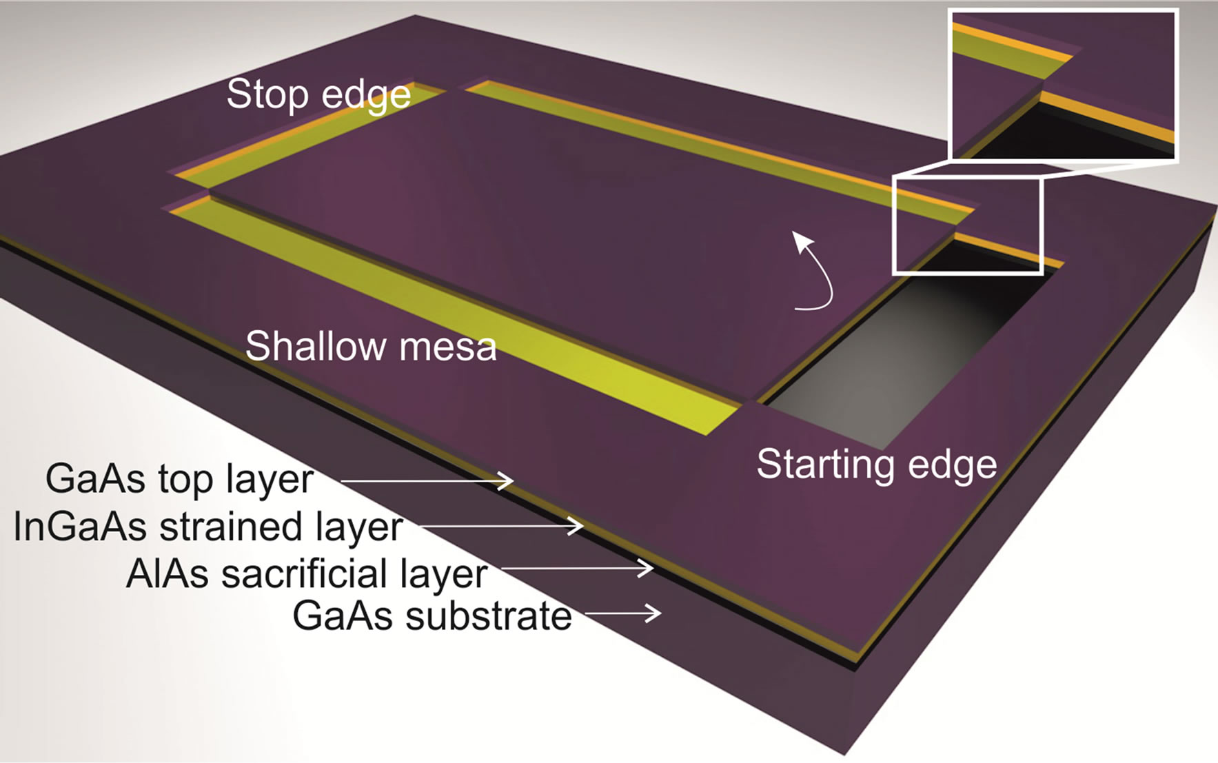
Figure 1. Sketch of the substrate. The starting edge is etched through the GaAs top layer and the InGaAs. The shallow mesa and stop edges are etched into the InGaAs layer. After selective etching of the AlAs sacrificial layer with HF the strained double layer starts rolling up. The rolling direction is marked with an arrow.
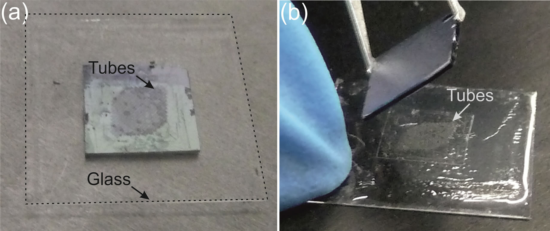
Figure 2. (a) GaAs sample placed on the glass substrate (black dashed line); (b) Separation of the glass substrate and the GaAs substrate with tubes lying on the glass substrate. The tubes on the GaAs substrate are released and transferred tubes on the glass substrate.
The first PDMS layer is important to provide a mechanically compliant layer, which will prevent the tubes from breaking during the transfer process. After baking, the substrate is spin coated again. This time the PDMS thickness has to be reduced to get layer thicknesses of 1µm or less, to avoid the tubes from sinking into the PDMS. This is achieved by using n-hexane. Applying an established technique, Thangawng et al. report on PDMS film thicknesses of 70 nm on a Si substrate [13]. The ratio of PDMS/n-hexane used in our experiments is 1:8, which delivers layer thicknesses of about 1 µm (Figure 3).
For the ease of transfer, the GaAs sample with microtubes on top is placed on the hot-plate at 100˚C and, after spin-coating the sample with PDMS/n-hexane for the second time for 1 minute at 8000 rpm, the glass-substrate is immediately placed on top of the GaAs sample (Figure 2).
After complete curing of the glass substrate, the sample is peeled off from the glass which will tear the tubes from the GaAs substrate and glue them to the glass. With this step the transfer process is completed.
2.3. Processing Bio-Compatible Samples
To use this kind of sample for experiments with living cells it is paramout that materials are made biocompatible. It is well known that arsenic is highly toxic [14]. In order to prevent cells from dying on such substrates, we process our samples with Parylene-C (Speciality Coating Systems PDS2010) after completing the transfer as reported recently for non-transferred microtubes [6]. This CVD process enables covering the tubes’ outer and inner surfaces, the achieved parylene thicknesses are in a range of around 160 nm.
3. Results/Discussion
During the development process, different methods for transferring the tubes were tested. As a first step, transferring of GaAs tubes onto a few mm thick PDMS layer was tested. This method delivered undefined results be-
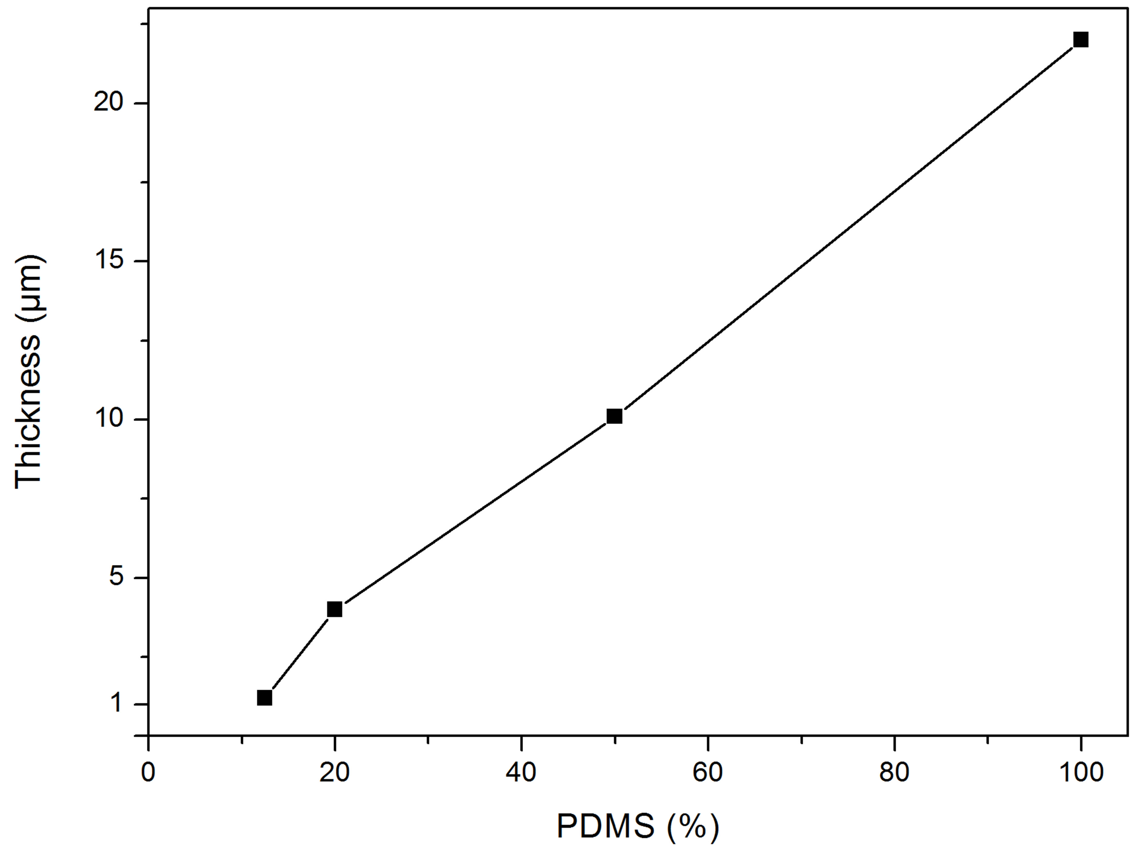
Figure 3. The layer thickness of PDMS/n-hexane plotted against the amount of PDMS in percent. The glass substrate was at first spin-coated with PDMS/curing agent (10:1) at 2000 rpm for one minute, baked on a hot-plate for two minutes at 100˚C. The second layer of PDMS/n-hexane was spincoated for 1 minute at 8000 rpm with PDMS percentage as indicated.
cause the PDMS layer cures unevenly on the hot-plate resulting in a larger chance that the tubes will sink into the PDMS. We thus began spin-coating the PDMS on glass cover-slips to obtain a well-defined layer thickness and increase the probability that the tubes will not sink into the liquid PDMS. When using a lower ratio of n-hexane to PDMS than 1:8 during the transferring process, PDMS bubbles appeared on the glass substrate.
By using a ratio of 1:8, formation of the bubbles is avoided and the surface between the tubes remains smooth. Another advantage of the spin-coating is the fact that, with this method, thinner substrates can be fabricated.
The yield of successfully transferred tubes was clearly dependent on the tubes length. For 75 µm long tubes an average of only a few percent of the tubes was transferred, while the yield was improved to 65% for 50 µm tubes (Figure 4). Considering the fact that on the whole sample we have about 5 × 10³ tubes initially in one fabrication step more than 3 × 10³ were transferred successfully.
As a next step, these samples will be used for guided neuron growth. After bio-compatibilizing the tubes [6], it is possible to guide neuronal growth through the tubes and create a neural network. In addition it is possible to investigate the growth of neurons on these transparent substrates with TIRFM.
4. Conclusion
In this letter we introduced a method of direct transfer of semiconductor microtubes to a transparent glass substrate. We reported that 65% of the microtubes from the GaAs
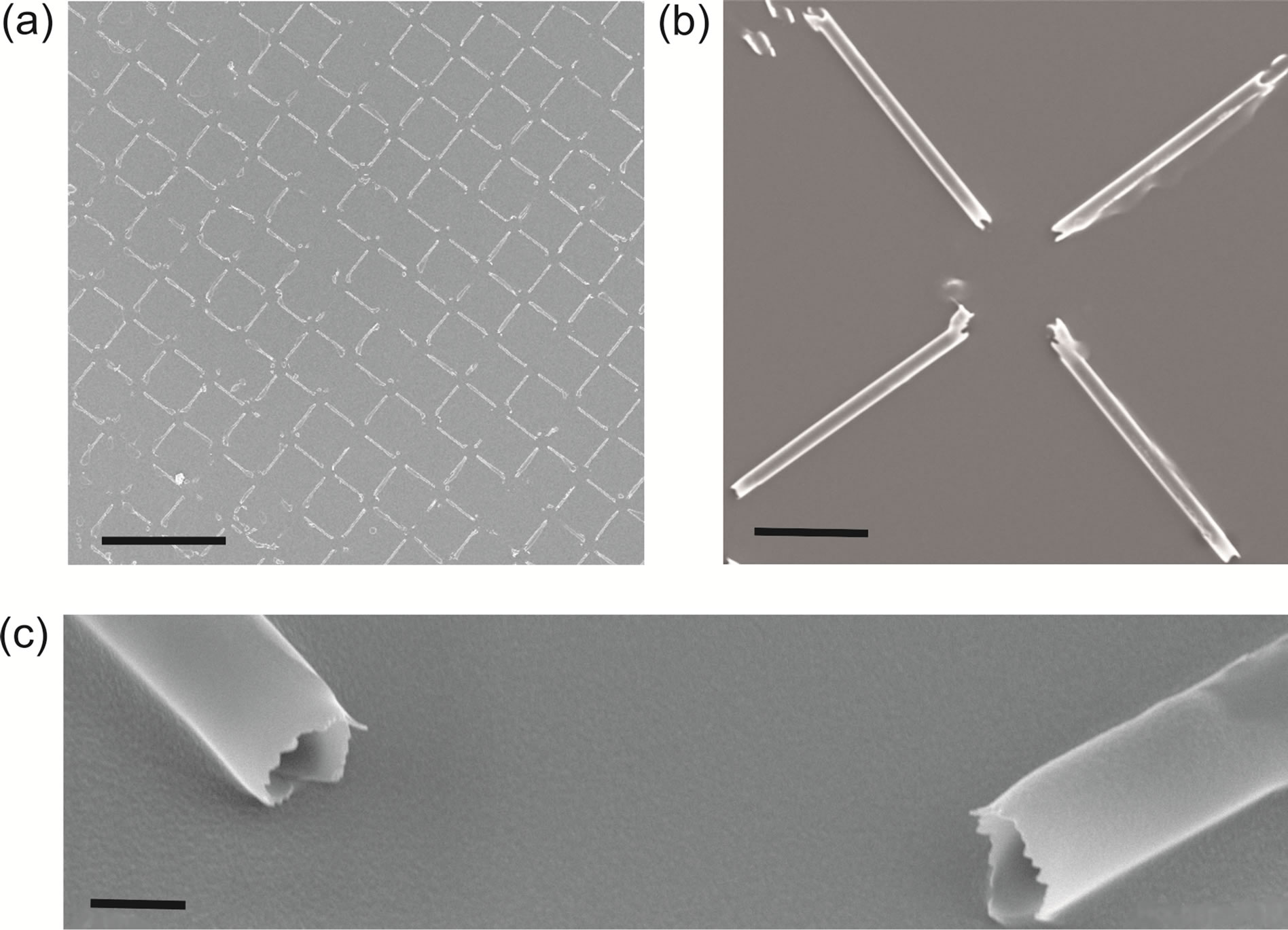
Figure 4. Array of microtubes lying on the glass substrate, (a) scale bar 200 µm. (b) close-up of (a), scale bar 20 µm. (c) close-up of (b), scale bar 2 µm.
substrate are transferred. These kinds of devices are applicable in several fields such as optoelectronics and experiments on cellular networks. The toxicity of GaAs is prevented by coating the tubes with Parylene-C in a CVD process. In the future, we plan to observe the microtube interactions with the overgrown neural networks.
5. Acknowledgements
We would like to thank the the Air Force Office of Scientific Research (AFOSR) for support through the MURI and the DFG for funding by grant HA2042/6-1 and GrK1286.
REFERENCES
- E. J. Smith, W. Xi, D. Makarov, I. Moench, S. Harazim, V. A. Bolaños Quiñones, C. K. Schmidt, Y. Mei, S. Sancheza and O. G. Schmidt, “Lab-in-a-Tube: Ultracompact Components for On-Chip Capture and Detection of Individual Micro-/Nanoorganisms,” Lab on a Chip, Vol. 12, No. 11, 2012, pp. 1917-1931. http://dx.doi.org/10.1039/c2lc21175k
- C. Strelow, H. Rehberg, C. M. Schultz, H. Welsch, C. Heyn, D. Heitmann and T. Kipp, “Optical Microcavities Formed by Semiconductor Microtubes Using a Bottlelike Geometry,” Physical Review Letters, Vol. 101, No. 12, 2008, Article ID: 127403. http://dx.doi.org/10.1103/PhysRevLett.101.127403
- T. Kipp, H. Welsch, C. Strelow, C. Heyn and D. Heitmann, “Optical Modes in Semiconductor Microtube Ring Resonators,” Physical Review Letters, Vol. 96, No. 7, 2006, Article ID: 077403. http://dx.doi.org/10.1103/PhysRevLett.96.077403
- S. Schwaiger, M. Bröll, A. Krohn, A. Stemmann, C. Heyn, Y. Stark, D. Stickler, D. Heitmann and S. Mendach, “Rolled-Up Three-Dimensional Metamaterials with a Tunable Plasma Frequency in the Visible Regime,” Physical Review Letters, Vol. 102, No. 16, 2009, Article ID: 163903. http://dx.doi.org/10.1103/PhysRevLett.102.163903
- M. Yu, Y. Huang, J. Ballweg, H. Shin, M. Huang, D. E. Savage, M. G. Lagally, E. W. Dent, R. H. Blick and J. C. Williams, “Semiconductor Nanomembrane Tubes: ThreeDimensional Confinement for Controlled Neurite Outgrowth,” American Chemical Society Nano, Vol. 5, 2011, Article ID: 2447.
- C. S. Bausch, A. Koitmäe, E. Stava, A. Price, P. J. Resto, Y. Huang, D. Sonnenberg, Y. Stark, C. Heyn, J. C. Williams, E. W. Dent and R. H. Blick, “Guided Neuronal Growtch on Arrays of Biofunctionalized GaAs/InGaAs Semiconductor Microtubes”.
- E. J. Smith, S. Schulze, S. Kiravittaya, Y. Mei, S. Sanchez and O. G. Schmidt, “Lab-in-a-Tube: Detection of Individual Mouse Cells for Analysis in Flexible Split-Wall Microtube Resonator Sensors,” Nano Letters, Vol. 11, No. 10, 2011, pp. 4037-4042. http://dx.doi.org/10.1021/nl1036148
- H. Tatsumi, Y. Katayama and M. Sokabe, “Attachment of Growth Cones on Substrate Observed by Multi-Mode Light Microscopy,” Neuroscience Research, Vol. 35, No. 3, 1999 pp. 197-206. http://dx.doi.org/10.1016/S0168-0102(99)00085-1
- C. Strelow, C. M. Schultz, H. Rehberg, M. Sauer, H. Welsch, A. Stemmann, C. Heyn, D. Heitmann and T. Kipp, “Light Confinement and Mode Splitting in Rolled-Up Semiconductor Microtube Bottle Resonators,” Physical Review B, Vol. 85, No. 15, 2011, Article ID: 155329. http://dx.doi.org/10.1103/PhysRevB.85.155329
- V. Y. Prinz, V. A. Seleznev, A. K. Gutakovsky, A. V. Chehovskiy, V. V. Preobrazhenskii, M. A. Putyato and T. A. Gavrilova, “Free-standing and Overgrown InGaAs/- GaAs Nanotubes, Nanohelices and their Arrays,” Physica E, Vol. 6, No. 1-4, 2000, pp. 828-831. http://dx.doi.org/10.1016/S1386-9477(99)00249-0
- M. Grandmann, “Nanoscroll Formation from Strained Layer Heterostructures,” Applied Physics Letters, Vol. 83, No. 12, 2003, pp. 2444-2446. http://dx.doi.org/10.1063/1.1613366
- O. Schumacher, S. Mendach, H. Welsch, A. Schramm, C. Heyn and W. Hansen, “Lithographically Defined metalSemiconductor-Hybrid Nanoscrolls,” Applied Physics Letters, Vol. 86, No. 14, 2005, Article ID: 143109. http://dx.doi.org/10.1063/1.1897056
- A. L. Thangawng, M. A. Swartz, M. R. Glucksberg and R. S. Ruoff, “Bond-Detach Lithography: A Method for Micro/Nanolithography by Precision PDMS Patterning,” Small, Vol. 3, No. 1, 2007, pp. 132-138. http://dx.doi.org/10.1002/smll.200500418
- M. Omura, A. Tanaka, M. Hirata, M. Zhao, Y. Makita, N. Inoue, K. Gotoh and N. Ishinishi, “Testicular Toxicity of Gallium Arsenide, Indium Arsenide, and Arsenic Oxide in Rats by Repetitive Intratracheal Instillation,” Toxicological Sciences, Vol. 32, No. 1, 1996, pp. 72-78.
NOTES
*Corresponding author.