Modern Instrumentation
Vol.2 No.2(2013), Article ID:30824,8 pages DOI:10.4236/mi.2013.22006
Scanning Head for the Apertureless near Field Optical Microscope
1University of Erlangen-Nuremberg, Erlangen, Germany
2Institue for Theoretical and Experimental Physics, Moscow, Russia
Email: kaza@itep.ru, heiner.ryssel@iisb.fraunhofer.de
Copyright © 2013 D. V. Kazantsev, H. Ryssel. This is an open access article distributed under the Creative Commons Attribution License, which permits unrestricted use, distribution, and reproduction in any medium, provided the original work is properly cited.
Received November 10, 2012; revised December 17, 2012; accepted December 27, 2012
Keywords: Near-Field Optics; Apertureless SNOM; Scanning Head
ABSTRACT
The design and characterization of a tip control unit for an apertureless scanning near field optical microscope (ASNOM) is reported. To make the instrument operation easier, the cantilever control parts (piezo excitation of the cantilever vibration for the dynamic mode feedback and the parts necessary for the optical lever scheme of the vibration control) were placed in a separate detachable assembly. To suppress the influence of vibrations of the setup, the assembly was made lightweight. Good optical access to the ASNOM tip from various directions is provided in the system. High long-term mechanical stability of the system (~50 nm lateral drift in 18 hours) as well as low sensitivity to seismic vibrations (~400 pm RMS) is demonstrated. It is shown that external sound is not a main source of noise in the topography image (~200 pm RMS). The light field distribution (with its amplitude and phase) around the ASNOM tip was acquired by scanning the focal spot around the tip, and a high optical quality of the system is demonstrated.
1. Introduction
A powerful tool for the local investigation of surface optical properties is apertureless scanning near field optical microscopy [1] ASNOM (scattering SNOM, s-SNOM). It is a modification of SNOM [2] in which the light scattered by an AFM [3] tip is collected. The tip in this instrument can be considered to be a macroscopic dipole antenna which re-emits the radiation to the environmental space due to dipole oscillations, excited in the tip by the external electromagnetic field. The “grounding” conditions of this antenna are determined by the “capacitor” of the slit between the tip and the surface being investigated. This is the reason why the ASNOM is able to provide a map representing the dielectric properties of the sample and the local field at the tip location. The lateral resolution of the instrument is determined by the tip radius. The tip which scatters the electromagnetic radiation is typically covered with a metal [4] due to its higher polarizability. The spatial resolution of the AS-NOM technique was proven to be as high as 1 nm [5], so that it seems to be sufficient to select nanoparticles [6], viruses [7] and even single molecules [8] on the sample surface for the investigations.
With exception of the tip-enhanced Raman spectroscopy [9-11], the light scattered by the tip has the same wavelength as the excitation light. In such a case the interferometer used to detect the signal [12], which was already mentioned in the very first paper on ASNOM, is a vital part [1]. Without it, the dynamic range of the photodetector may be not sufficient [13] to recognize the signal component caused by the really near-field (non-radiative) part of the tip-sample electromagnetic interaction. The method allows, due to implementation of the interferometer detecting scheme, to store both amplitude and phase [14,15] of the light scattered by the tip. Most ASNOMs are experimental setups [13,16,17], but there are also commercially available versions [18]. There are several artifacts which distort the data collected with the help of ASNOM. First, the optical signal recovered at the oscillation frequency of the tip [19] results mainly from scattered light caused by the interference between the tip and its image in the surface. These variations of the photocurrent are useless in the terms of near-field (nonradiative) electromagnetic interaction of the tip and the surface. To get rid of this background, the signal must be recovered using higher harmonics of the tip oscillation frequency [20], because the modulation of the tip polarizability caused by the non-radiative electromagnetic tip-sample interaction is the only effect in the system which depends in a non-linear way on the tip position.
Second, the ASNOM is rather sensitive [21] to the polarization of the light driving the tip (the E-vector must be along the tip, i.e. normal to the surface). In some home-built [16,17] and commercial [22,23] systems the light comes along the tip i.e. normally to the surface. In such a geometry just a small fraction of the focused radiation is able to excite the dipole oscillations along the tip, namely that focal cone beam fraction which illuminates the tip from aside due to the high numerical aperture of the objective used. The optical signal acquired in such a geometry is rather weak. Operation of the ASNOM is based on demodulation of the tip scattering variations caused by the tip tapping motion, which means that the conditions of the tip mechanical oscillation affect strongly the amplitude and phase of the recovered optical signal. In principle, the cantilever bending can be used for the lock-in reference [13], but not all lock-in models are able to track the fast variations of the reference signal phase. Also, the variations in the tip-sample bounce conditions (which are strongly nonlinear in the terms of the tip oscillation, see e.g. [24,25]) may affect significantly the amplitude of the nearfield component in the scattered light variations. Unavoidable mechanical vibrations, caused by the water cooling of the main laser and acoustical-optical modulator in the heterodyne interferometer detection scheme, are present in the setup. Therefore, the tip oscillation conditions have to be rather well stabilized by the feedback, which is not always the case.
Another requirement to the scanning head being designed is obviously its ability to allow the optical access to the tip. The coherent light beam is focused onto the tip, and the light scattered by the tip is collected back to the interferometer. The probing beam must come along the surface, but not completely parallel to it (the efficiency of the dipole antenna located near the ground plane is zero in the exactly “horizontal” direction, see [21]). One also has to keep in mind to provide optical access to the sample from the top or from the substrate, so that the mechanical parts of the scanning head must not shadow the beams.
Possibly, the problems mentioned above explain why ASNOM still did not get out of the stage “nice trick providing sharp lateral resolution”, to the state of widely used instrument, providing the quantitative data. Just a few papers are devoted to the design and utilization of ASNOMs.
The aim if this work was to make a user-friendly, flexible ASNOM system for everyday’s use in the research lab. In particular, it means that 1) sample loading, optical alignment and operation must be simple; 2) the fabrication of the hand-made tips (see e.g. [17,19]) should be excluded from the operation; the commercial tips should be used instead.
2. Mechanical Design
2.1. General Approach
A schematic view of the scanning head which fulfills the requirements listed above is presented in Figure 1.
The tip is always fixed in the focus of the objective, so that the amplitude-phase conditions of the tip scattering in the optical path of the interferometer are constant. The focus of the work beam is aimed onto the tip by the objective XYZ translation stage during the initial setup alignment after the cantilever chip is reloaded. The optical nature of the ASNOM experiments brings some special requirements to the mechanical design, compared to the other SPM techniques. Namely, an optical access has to be provided from many different directions. The requirement to make the instrument to be wavelength- independent leads to the implementation of a mirror [26] instead of a lens to focus the external probing beam onto the cantilever. The option to choose the area on the sample surface under visual control, as well as the option to implement a high-NA objective to collect the radiation scattered in the direction normal to the sample surface has to be implemented. Also, the experimental geometry, in which the tip vicinity area is illuminated from beneath the sample, was included as a possible mode of operation. To make operation convenient, tip replacement, sample replacement, and the optical realignment procedures were designed to reduce their interaction as much as possible.
2.2. Sample Raster Scanning and “Height” Positioning
The raster scanning of the surface is provided by a com-

Figure 1. Cross-sectional view of the tip scattering microscope scanning head. The cantilever control unit lays on the base slab, and the sample is fixed on the scanner flange, which comes from beneath of that slab through appropriate hole in it. The sample positioning parts (Z-approach and lateral transfer) are not shown.
mercial scanner P-541 (Physik Instrumente, GmbH, Germany). The control electronics includes additional feedback loop, based on the XY displacement capacitive sensors integrated in the scanner table. At the same time, the sample positioning normal to the surface is provided by three piezos, which drive up/down thin and lightweight coin-like sample holder under the control of the dynamic mode AFM feedback system. This allows to achieve a rather large feedback loop bandwidth which is limited in this case just by the mass of the parts involved in the motion normal to the surface. At the expense of reduced metrological quality, such a solution allows to set faster scanning speed values, without damage to the cantilever and without noticeable variations in the tipsample interaction conditions.
To provide a coarse tip-sample approach, the scanner is driven upwards and downwards together with the sample fixed on the top of it. The approach is provided by three screws with contact spheres on their ends, driven by three step motors. No plates or levers were necessary to be installed between the motor-driven screw shafts and the point balls fixing the scanner. As it is shown below, the topography noise and long-term stability of the system is very good. These three approach screws are fixed on the base plate by the traditional way “hole-slit-plane”. To choose the sample area being scanned, the piezo scanner is mounted on top of the flat XY micrometer stage (OWIS GmbH).
2.3. Cantilever Control Assembly
The cantilever bending oscillation is excited by a small piezo, driven at the cantilever resonance frequency. Commercial AFM cantilevers (Budget Sensors and Micro Masch) covered by platinum were used. The cantilever deflection sensor is based on the optical lever principle [27,28]. The beam of a small semiconductor laser with feedback-controlled output power (SPMC01, Power Technologies Inc., 1 mW at 670 nm) is focused onto the back side of the cantilever. To bring the focal spot onto the cantilever, the laser is fixed in a tilting-type kinematic mount. This control beam, being reflected from the cantilever, is redirected by the mirror onto a quad photodiode pad, so that the spot displacement on the photodiode is determined by the cantilever deformation. The mirror which redirects the beam onto the quad photodiode is also fixed on a tilting-type mount. These two custommade alignments make it easy to compensate the cantilever spatial and angular position tolerance after a cantilever replacement. The photodiode is mounted in a holder, which allows its rotation around the beam direction. Thus, it is possible to optimize the setup, by alignment of the photodiode segments along the lateral trajectory of the beam spot to separate “lateral force” and “normal force” signals.
The conventional AFM optical lever electronics was splitted into two PCBs. To reduce the heat dissipation on the AFM head as well as its weight, most of the electronics (“normal” and “lateral” difference stages, sum stage, analog divider(s), buffer stages for the tip vibration piezoplate excitation, tip bias control, voltage regulators for the OpAmps, diode laser, and quad photodiode bias) are mounted on the PCB located 10 - 15 cm apart. The transimpedance stages are mounted on the same small PCB (11 mm diam) on which the quad photodiode is located. Therefore, the bandwidth of the optical lever sensor is at least 3 MHz, and allows to monitor quantitatively the non-linearities in the tip oscillation. It means also that the phase of the observed tip oscillation contains no parasite shift for the frequencies below approx. 1 MHz, due to the Kramers-Kronig relations.
To leave open the optical path from the top to the sample surface, the laser beam of the cantilever control is declined at 45˚ to the vertical axis of the setup. This geometry reduces the sensitivity of the control by 30%, but this plays just a minor role, because the noise level of the setup is low enough. The angular shape of the probe beam in the optical lever scheme is far from being perfectly circular. It is close to elliptical with an excentricity of about 1:6. Simultaneously, the focus of the beam is also elongated in its shape. By focusing the spot onto the cantilever along its axis [29], we get an additional possibility to improve the sensitivity of the cantilever control scheme. The narrower the angular shape of the reflected beam, the higher the sensitivity of the quad photodiode scheme, regardless to the distance from the cantilever [30].
The parts related to the AFM operation were assembled in a stiff unit (See Figures 1 and 2). Once aligned after a new cantilever is glued onto the piezo-driven cantilever holder, the assembly does not require any optical realignment and sensor sensitivity recalibration even if it is removed from the system for sample reloading. The position of the cantilever control assembly is determined by three radial slits in its bottom surface, corresponding
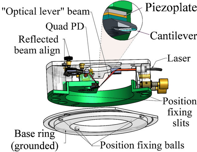
Figure 2. Cantilever control assembly of the ASNOM head.
to three steel bearing balls, pressed into the adapter ring. The ring is fixed, in turn, on the base slab. The precision of the tip position in the focus after reinstallation of the cantilever control assembly is better than 1 μm.
2.4. Lightweight but Stiff Tip Holder
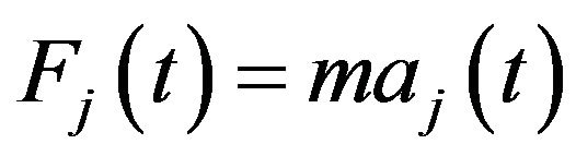
To suppress the sensitivity of the instrument to vibrations of the optical table, the cantilever assembly was designed to be very lightweight and stiff. The optical table is much heavier than the scanning instrument, so we assumed the “seismic” noise motion of the optical table to be completely independent on the presence of the scanner. Therefore, the seismic noise can be described just by the following vibration law
 , (1)
, (1)
and consequently
 (2)
(2)
where vj(t), and aj(t), denote velocity and acceleration of the optical table, respectively (here . In such a model (See Figure 3), the vibration of the main optical table can be considered as just the noise in the weight of the parts (in particular, of the tip holder). The external inertial force applied to the part is expressed as
 . Below the tip holder resonant frequency, the less the mass of the parts, the less the system sensitivity to external vibrations. On the other hand, the higher the stiffness of the tip holder assembly, the less the sensitivity of the system to external vibrations. In our model, the largest contribution to the tip-sample separation distance is provided by the tip carrier unit of the mass m, with the rigidity characterized by the value k (the softest mechanical link in the system, including also the elasticity of the tip holder parts themselves, see Figure 3). There-

Figure 3. Model of the instrument to consider its sensitivity to the vibration of the main optical table. The stiffness K of the sample holder is considered to be much higher than the stiffness k corresponding to the tip holder parts.
fore, the sensitivity of the tip control assembly to the external vibrations can be expressed by the ratio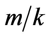 . In contrast to other systems [22,31-34], we designed this assembly to be lightweight, wide, and rigid. The low mass of the tip control assembly reduces sensitivity of the tip-sample position to the vibrations of the base, wide feet span prevents it from the wobbling mode of displacement, walls and frames prevent it from the membrane-like modes of oscillation.
2.5. Cantilever or Tuning Fork?
There are clear reasons why the AFM-like cantilever should be strongly preferred to the tuning fork in the case of ASNOM design. The demodulation of the interferometer output signal at higher harmonics of the tip tapping frequency is used in ASNOM. The recovery of the signal part related solely to the near-field optical interacttion of the tip and surface in the scattered radiation requires to provide a clear difference between the states “close” and “far” of the tip. Therefore, the larger the tip oscillation amplitude, the more pronounced the collected near-field-optical signal. Practically, an amplitude of 40 - 60 nm is used with solid state samples. In such a case, the forces arising at the moment of the tipsurface impact are rather high, so that it may lead to a tip destruction and cause fast wearing of the probe. The typical mass of the AFM cantilever is much less than the mass of the tuning fork prong which can be estimated by the dimensions of the objects: the dimensions of the cantilever are about 3 × 30 × 200 m3 while the prong of the tuning fork has dimensions of approx. 500 × 500 × 3000 m3. Usually, these two mechanical oscillators have a similar resonant frequency (30 - 100 kHz) which means that the forces to drive the mass of the oscillating part are much larger in the case of the tuning fork. Thus, to modify noticeably the amplitude/phase of the probe oscillation much more energy is needed every cycle in the case of the tuning fork oscillator.
Since AFM cantilever is chosen as the concept, the optical lever (beam deflection) is the optimum solution to monitor the cantilever oscillation. It is sensitive, simple, reliable, and it does not require any special measures as piezoresistive cantilevers do [35]. In addition, it is sensitive to the DC-mode deflections of the cantilever (and that can be utilized for the absolute calibration of the tip displacement by the scanning of the grating sample with a known step height). These various reasons make the AFM cantilever monitored by the optical lever scheme an optimum solution for the flexible application.
3. Characterization
3.1. Topography Noise Level
The mechanical quality of the system is demonstrated in Figure 4 where the AFM image of a DNA molecule on a mica substrate is shown. The characteristic deviation in the topography height histogram (unfiltered) is about 0.34 nm (See Figures 4(a) and (b)). The RMS deviation of the height error signal is 0.26 nm (See Figures 4(c) and (d)). It should be pointed out, that the image was obtained in the presence of vibrations caused by a water pump.
These results prove that the concept “light but stiff tip holder on a heavy base” which we kept, in order to suppress the influence of external vibrations. The map of the tip vibration amplitude and its histogram (observed simultaneously with topography) is also presented in Figure 4. One can see that the level of the tip-sample contact is kept rather stable in the experiment. The noise properties of the cantilever control unit alone (without tipsample contact) are even better. The RMS deviation of the vibration amplitude measured without contact to the surface is no more than 0.07 nm.
One could expect, as a side effect of the general concept “heavy basement - lightweight roof”, a sensitivity of the instrument to acoustic noise (microphone effect). This matter was taken into account during the characterization and implementation of the instrument. It was observed that sometimes the human speech near the setup can be found in the topography map, as additional noise of no more than 0.2 nm RMS. It was found that the cantilever control assembly itself has no noticeable sen-
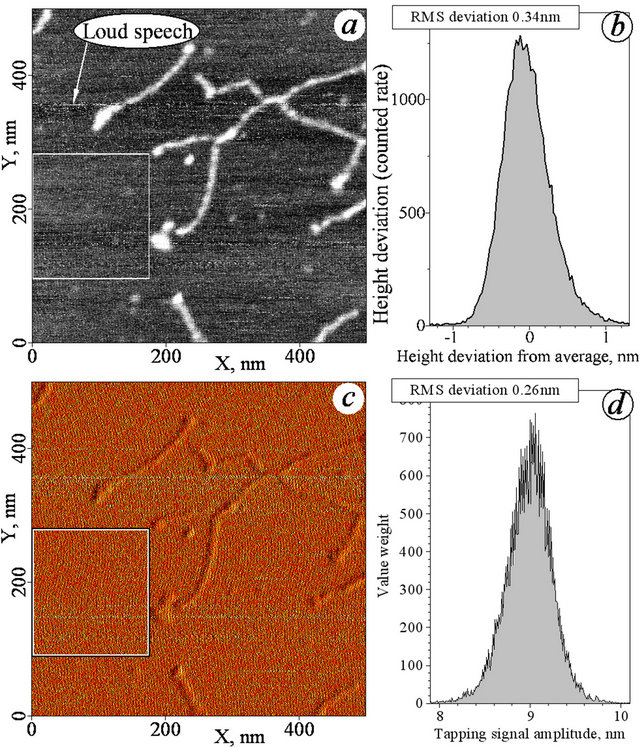
Figure 4. DNA image on a mica substrate. (a) Topography image; (b) Height histogram of the free mica area; (c) Tip vibration sensor signal amplitude; (d) Amplitude histogram of the same area. Feedback setpoint corresponds to 10nm of the vibration amplitude for this cantilever.
sitivity against the acoustic noise. There is also almost no microphone effect in the DC mode of the feedback, in which the tip displacement is directly used as the feedback input. The microphone effect appears mainly if the tip-sample distance is stabilized by the feedback in dynamic mode. One can explain this by the strong nonlinearity of the tip-sample interaction potential, and by the high value of the cantilever quality factor Q. To quench the oscillation, just a single period of the cantilever frequency might be enough (nonlinear effect), while stable amplitude and phase of the driven oscillation of the cantilever gets restored only after approximately Q oscillation cycles (linear effect). It was found that the sensitivity mainly depends on the way how the sample (7 × 7 × 0.5 mm3, or even 10 × 10 × 0.15 mm3 in the case of mica substrate) is fixed on the holder. In any case the acoustic sensitivity of the instrument is sufficiently low, and acoustic noise is by far not the main source of noise in the system. An acoustic isolation cage during operation is, therefore, not necessary.
3.2. Long-Time Mechanical Stability
The ASNOM images of metal dots (Au) on the dielectric surface (quartz) taken with an interval of 18 hours with no adjustment of the setup are presented in Figure 5.

Figure 5. The map of the near field component of the tip scattering, recovered at 3rd harmonic of the tapping frequency Ω. Scan area is 4.5 × 4.5 μm2. The images of metal (Au) structure array on dielectric substrate were taken with 18 hour interval. Wavelength is 633 nm.
The light scattered by the tip was detected by the interferometer at the wavelength of 633 nm. A Mach-Zehnder-like interferometer heterodyne scheme was used [14] with demodulation of the interferometer output signal at a frequency corresponding to the third harmonic of the tip oscillation. One can see that there is no significant drift of the surface with respect to the tip during that period; the presence of the clear light scattering signal in the second image means also that the tip does not drift away from the caustic of the main beam focus (which has a characteristic size of about the wavelength used, namely 600 - 800 nm).
3.3. The Light Field Distribution around the Tip
In many practical applications it is very useful to know the real configuration of the electromagnetic field at the very tip vicinity. Figure 6 represents the map of the scattered light amplitude and phase in the case when the tip stays fixed in respect to the sample while the focus of the main beam objective scans around the position of the best scattering signal. The mapping was performed using a crystalline SiC sample which provides a strong enhancement of the tip scattering at the CO2 laser band due to the presence of lattice resonance. The smooth variation of the amplitude shows an independence of the amplitude output on the signal phase. The period in the phase variations corresponds to the geometrical change of the optical path from the interferometer to the tip, due to the objective positioning. In particular, the phase period p0 = 8.3 μm in the section corresponding to the purely vertical motion of the objective (perpendicular to the beam of the interferometer signal arm) corresponds to an angle (≈40˚) of the deflection in the vertical plane: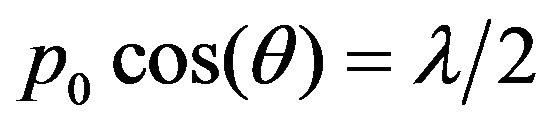 . The ramp-like phase behavior is simply caused by the change of the optical path from the interferometer to the tip, due to the objective motion. The scattering amplitude and phase images demonstrate a high quality of the wave fronts in the tip irradiating beam. It means that the tip illumination conditions can be well described by a plane wave. It is important in such experiments, in which the tip is just a probe to measure the collective response of the surface, e.g. in the investigations of the surface polariton waves.
4. Known Problems
4.1. Focus Position Drift
The instrument is very sensitive to the focus position of the light beam on the tip (i.e. the focus of the light being used for the tip-scattering in the experiment, not the additional beam to monitor the AFM cantilever deflection). Due to the interference origin of this sensitivity (the light scattered by the tip is detected afterwards with the help of the interferometer), the mechanical stability of the tip
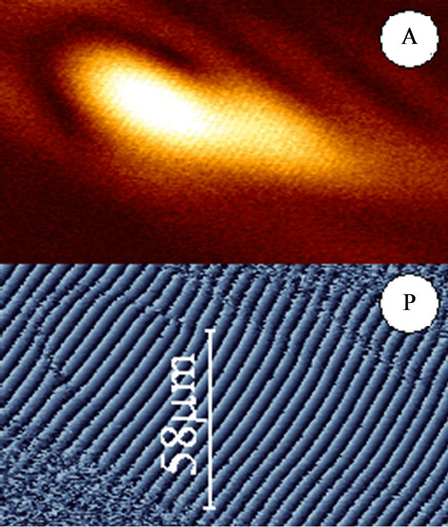
Figure 6. The variations in the detected second harmonic component amplitude (A) and phase (P), caused by the objective mirror scanning. The Pt-coated tip is brought to a contact with the SiC surface under the feedback control. No lateral scanning signal is applied to the sample/tip piezo table. Vertical axis corresponds to the vertical motion of the objective (perpendicular to the interferometer arm beam) horizontal direction is along the cantilever. Objective scan span is 95 × 95 μm2. Wavelength is 10.85 μm.
position in the main beam focus is more critical at the visible wavelength band and less important at the infrared band.
4.2. Light Polarization
The polarization of the electromagnetic radiation which excites the response of the scattering tip (modulated with the tip tapping frequency due to the tip-sample near-field interaction being investigated) has to be always normal to the surface. The tip acts just as an antenna rod in conventional radiophysics, so its ability to scatter the radiation (as well as its sensitivity to the driving electromagnetic field) is maximum if the E vector of the driving field is parallel to the tip’s long axis.
4.3. Signal Recovery
The subject of the acquisition in the ASNOM setup are the higher harmonics of the tip tapping oscillation frequency in the detector photocurrent. DC component and fundamental do not carry any relevant information. The amplitude of the useful component in the detector signal is, typically, more than 100 times less than the amplitude of the parasitic signals in the interferometer’s detector photocurrent caused by the tip oscillation and by other displacements of the parts. Even in the best case of strong resonant dielectric response of the sample the useful component in the detector output is hardly visible on the screen of the oscilloscope. Thus, one should have a very good idea about the expected signal. The subjects of acquisition are relatively short variations of the photocurrent which occur mainly at the very moment when the tip-sample distance is minimum.
One must keep in mind that the photocurrent of the detector in the interferometer is proportional to the intensity of the field. The variations in the photocurrent, although they are being caused by the same modification of the tip scattering amplitude/phase, depend strongly on the reference beam phase. The length of the reference arm is initially arbitrary in the interferometer. To avoid that, the average over the reference beam phase is necessary for each ASNOM map point [1,14]. Phase-sensitive lock-in recovery at the difference frequency must be arranged using the “heterodyne” scheme [13,14] (in case if Mach-Zehnder-like interferometer with acoustical-optical scattering is used), or phase modulation [15] (in case a Michelson interferometer scheme is used) has to be implemented to average the recovered signal over all possible phases of the reference beam. In general the Michelson interferometer is preferable for the ASNOM operation, because its alignment is wavelength-independent.
4.4. Data Interpretation
The amplitude of the light scattered by the tip (mainly scattered by the tip and the cantilever, with a tiny additional fraction caused by the tip-sample near-field interaction at the moment of the very contact) is a product of the local electromagnetic field at the tip location and of rather complicated expressions containing the tip/sample dielectric value, tip radius and the distance from the tip to the surface. In case all these values vary due to the tip oscillation, the final image data, consisting of recovered higher harmonic components, may become rather difficult to be interpreted.
5. Conclusion
A cantilever control unit for the operation of an ASNOM was designed and characterized. The requirements specific for ASNOM operation (wide optical access, good optical stability) were fulfilled. The design concept (framelike light-weight detachable assembly), contrary to the common style (compact and relatively heavy assembly), was proven to be successful. The sensitivity of the instrument against vibrations was successfully suppressed. Fast (seismic-like vibrations) and long-term (thermal drift) noises were proven to be low enough. The instrument is wavelength-independent. Its operation was demonstrated in visible (λ = 633 nm) and mid-IR (λ ≈ 10.6 μm) light bands.
6. Acknowledgements
The author thanks Dr. Keilmann and Dr. Hillenbrand for their advising during the work presented, Dr. Ocelic who fabricated the non-linear signal recovery electronics, and Mr. Gatz for his perfect mechanical works. The author gratefully acknowledges funding of the Erlangen Graduate School in Advanced Optical Technologies (SAOT) in the framework of the excellence initiative. The work was supported by the German National Science Foundation (DFG grant KA3105/1-1).
REFERENCES
- F. Zenhausern, M. P. O’Boyle and H. K. Wickramasinghe, “Apertureless Near-Field Optical Microscope,” Applied Physics Letters, Vol. 65, 1994, No. 13, pp. 1623-1625. doi:10.1063/1.112931
- E. Betzig, M. Isaacson and A. Lewis, “Collection Mode Near-Field Scanning Optical Microscopy,” Applied Physics Letters, Vol. 51, No. 25, 1987, pp. 2088-2090. doi:10.1063/1.98956
- G. Binnig, C. F. Quate and C. Gerber, “Atomic Force Microscope,” Physical Review Letters, Vol. 56, No. 9, 1986, pp. 930-933. doi:10.1103/PhysRevLett.56.930
- U. C. Fischer and D. W. Pohl, “Observation of SingleParticle Plasmons by Near-Field Optical Microscopy,” Physical Review Letters, Vol. 62, No. 4, 1989, pp. 458- 461. doi:10.1103/PhysRevLett.62.458
- F. Zenhausern, Y. Martin and H. K. Wickramasinghe, “Scanning Interferometric Apertureless Microscopy: Optical Imaging at 10 Angstrom Resolution,” Science, Vol. 269, No. 5227, 1995, pp. 1083-1085. doi:10.1126/science.269.5227.1083
- A. Cvitkovic, N. Ocelic, J. Aizpurua, R. Guckenberger and R. Hillenbrand, “Infrared Imaging of Single Nanoparticles via Strong Field Enhancement in a Scanning Nanogap,” Physical Review Letters, Vol. 97, No. 6, 2006, Article ID: 060801. doi:10.1103/PhysRevLett.97.060801
- M. Brehm, T. Taubner, R. Hillenbrand and F. Keilmann, “Infrared Spectroscopic Mapping of Single Nanoparticles and Viruses at Nanoscale Resolution,” Nano Letters, Vol. 6, No. 7, 2006, pp. 1307-1310. doi:10.1021/nl0610836
- Y. Martin, F. Zenhausern and H. K. Wickramasinghe, “Scattering Spectroscopy of Molecules at Nanometer Resolution,” Applied Physics Letters, Vol. 68, No. 18, 1996, pp. 2475-2477. doi:10.1063/1.115825
- R. Stöckle, Y. Suh, V. Deckert and R. Zenobi, “Nanoscale Chemical Analysis by Tip-Enhanced Raman Spectroscopy,” Chemical Physics Letters, Vol. 318, No. 1-3, 2000, pp. 131-136. doi:10.1016/S0009-2614(99)01451-7
- L. T. Nieman, G. M. Krampert and R. E. Martinez, “An Apertureless Near-Field Scanning Optical Microscope and Its Application to Surface-Enhanced Raman Spectroscopy and Multiphoton Fluorescence Imaging,” Review of Scientific Instruments, Vol. 72 No. 3, 2001, pp. 1691- 1699. doi:10.1063/1.1347975
- B. Pettinger, B. Ren, G. Picardi, R. Schuster and G. Ertl, “Nanoscale Probing of Adsorbed Species by Tip-Enhanced Raman Spectroscopy,” Physical Review Letters, Vol. 92, No. 9, 2004, Article ID: 096101. doi:10.1103/PhysRevLett.92.096101
- J. S. Batchelder and M. A. Taubenblatt, “Interferometric Detection of Forward Scattered Light from Small Particles,” Applied Physics Letters, Vol. 55, No. 3, 1989, pp. 215-217. doi:10.1063/1.102268
- A. Bek, R. Vogelgesang and K. Kern, “Apertureless Scanning near Field Optical Microscope with Sub-10 nm Resolution,” Review of Scientific Instruments, Vol. 77, No. 4, 2006, Article ID: 43703. doi:10.1063/1.2190211
- R. Hillenbrand and F. Keilmann, “Complex Optical Constants on a Subwavelength Scale,” Physical Review Letters, Vol. 85, No. 14, 2000, pp. 3029-3032. doi:10.1103/PhysRevLett.85.3029
- N. Ocelic, A. Huber and R. Hillenbrand, “Pseudoheterodyne Detection for Background-Free Near-Field Spectroscopy,” Applied Physics Letters, Vol. 89, No. 10, 2006, Article ID: 101124. doi:10.1063/1.2348781
- G. Wurtz, R. Bachelot and P. Royer, “A Reflection-Mode Apertureless Scanning Near-Field Optical Microscope Developed from a Commercial Scanning Probe Microscope,” Review of Scientific Instruments, Vol. 69, No. 4, 1998, pp. 1735-1743. doi:10.1063/1.1148834
- R. Bachelot, P. Gleyzes and A. C. Boccara, “ReflectionMode Scanning Near-Field Optical Microscopy Using an Apertureless Metallic Tip,” Applied Optics, Vol. 36, No. 10, 1997, pp. 2160-2170. doi:10.1364/AO.36.002160
- Neaspec GmbH. http://www.neaspec.com
- A. Lahrech, R. Bachelot, P. Gleyzes and A. C. Boccara, “Infrared Reflection-Mode Near-Field Microscopy Using an Apertureless Probe with a Resolution of λ/600,” Optics Letters, Vol. 21, No. 17, 1996, pp. 1315-1317. doi:10.1364/OL.21.001315
- M. Labardi, S. Patanè and M. Allegrini, “Artifact-Free Near-Field Optical Imaging by Apertureless Microscopy,” Applied Physics Letters, Vol. 77, No. 5, 2000, pp. 621- 623. doi:10.1063/1.127064
- O. J. F. Martin and C. Girard, “Controlling and Tuning Strong Optical Field Gradients at a Local Probe Microscope Tip Apex,” Applied Physics Letters, Vol. 70, No. 6, 1997, pp. 705-707. doi:10.1063/1.118245
- NT-MDT (Moscow) NTegra SNOM System. http://www.ntmdt.com/device/ntegra-spectra
- JPK GmbH, TAO SNOM System. http://www.jpk.com/tao.download.61f23e409a2a8af9654595a415025092.pdf
- U. D. Schwarz, H. Hölscher and R. Wiesendanger, “Atomic Resolution in Scanning Force Microscopy: Concepts, Requirements, Contrast Mechanisms, and Image Interpretation,” Physical Review B, Vol. 62, No. 19, 2000, pp. 13089-13097. doi:10.1103/PhysRevB.62.13089
- F. J. Giessibl, “Advances in Atomic Force Microscopy,” Reviews of Modern Physics, Vol. 75, No. 3, 2003, pp. 949-983. doi:10.1103/RevModPhys.75.949
- F. Keilmann and R. Hillenbrand, German Patent DE10- 2006002461A1.
- G. Meyer and N. M. Amer, “Novel Optical Approach to Atomic Force Microscopy,” Applied Physics Letters, Vol. 53, No. 12, 1988, pp. 1045-1047. doi:10.1063/1.100061
- S. Kitamura and M. Iwatsuki, “Observation of 7 × 7 Reconstructed Structure on the Silicon (111) Surface Using Ultrahigh Vacuum Noncontact Atomic Force Microscopy,” Japanese Journal of Applied Physics, Vol. 34, Part 2, No. 1B, 1995, pp. L145-L148. doi:10.1143/JJAP.34.L145
- US Patent RE37, 299E.
- C. Putman, B. Grooth, N. Hulst and J. Greve, “A Detailed Analysis of the Optical Beam Deflection Technique for Use in Atomic Force Microscopy,” Journal of Applied Physics, Vol. 72, No. 1, 1992, pp. 6-12. doi:10.1063/1.352149
- G. Merritt, E. Monson, E. Betzig and R. Kopelman, “A Compact Fluorescence and Polarization Near-Field Scanning Optical Microscope,” Review of Scientific Instruments, Vol. 69, No. 7, 1998, pp. 2685-2690. doi:10.1063/1.1148999
- P. G. Gucciardi, M. Labardi, S. Gennai, F. Lazzeri and M. Allegrini, “Versatile Scanning Near-Field Optical Microscope for Material Science Applications,” Review of Scientific Instruments, Vol. 68, No. 8, 1997, pp. 3088-3092. doi:10.1063/1.1148246
- A. Naber, H.-J. Maas, K. Razavi and U. C. Fischer, “Dynamic Force Distance Control Suited to Various Probes for Scanning Near-Field Optical Microscopy,” Review of Scientific Instruments, Vol. 70, No. 10, 1999, pp. 3955- 3961. doi:10.1063/1.1150019
- Nanosurfr Mobile S Atomic Force Microscope.
- M. Tortonese, R. C. Barrett and C. F. Quate, “Atomic Resolution with an Atomic Force Microscope Using Piezoresistive Detection,” Applied Physics Letters, Vol. 62, No. 8, 1993, pp. 834-836. doi:10.1063/1.108593