Advances in Materials Physics and Chemistry
Vol.4 No.5(2014), Article ID:46474,12 pages
DOI:10.4236/ampc.2014.45012
Influence of Sn Low Doping on the Morphological, Structural and Optical Properties of ZnO Films Deposited by Sol Gel Dip-Coating
Chewki Zegadi1*, Khalil Abdelkebir2, Denis Chaumont2, Mohamed Adnane1, Saad Hamzaoui1
1Laboratory of Electron Microscopy and Materials Sciences, University of Science and Technology of Oran, El-Mnaouer Oran, Algeria
2Nanoform—ICB, Université de Bourgogne, Dijon, France
Email: *chouckizegadi@gmail.com, mohamed67adnane@gmail.com, hamzaoui.saad@gmail.com, khalil_abdelkebir@yahoo.com, denis.chaumont@u-bourgogne.fr
Copyright © 2014 by authors and Scientific Research Publishing Inc.
This work is licensed under the Creative Commons Attribution International License (CC BY).
http://creativecommons.org/licenses/by/4.0/


Received 10 April 2014; revised 15 May 2014; accepted 23 May 2014
ABSTRACT
In this work, Undoped Zinc Oxide (ZnO) and Sn-doped Zinc Oxide (ZnO:Sn) films have been deposited by sol-gel dip coating method, where the Sn/Zn atomic ratio was 3% and 5% in the solution. The effects of Sn incorporation on morphological, structural and optical properties of ZnO films were investigated. The Scanning Electron Microscopy (SEM) showed that the morphological surface of the films was affected by Sn low doping. The X-Ray Diffraction (XRD) patterns showed that all films have polycrystalline structures, and the doping incorporation has not lead to substantial changes in the structural characteristics of ZnO films. The crystallite size was calculated using the well-known Scherrer’s formula and found to be in the range of 23 - 40 nm. The measurements from UV-Visible Spectrophotometer (U-Vis) indicated that the highest average optical transmittance in the visible region was related to Undoped ZnO film, then the optical band gap and Urbach energy values of thin films were calculated. The X-Ray Photoelectron Spectroscopy (XPS) has demonstrated that Sn is incorporated in ZnO lattice.
Keywords:Sol-Gel Dip-Coating, ZnO Films, Sn Low Doping, SEM Micrographs, X-Rays Patterns, Optical Properties, XPS Spectrum

1. Introduction
Zinc Oxide (ZnO) thin film has been extensively studied for their attractive properties in electronic and optoelectronic applications [1] such as rectifiers, filters, resonators for radio communications and image processing [2] -[4] . Thin films of Zinc Oxide can also be used in chemical sensors which are highly sensitive gas detectors [5] [6] . Recently, Sn-doped ZnO (ZnO:Sn) has attracted great attention because it can expand the applications of Undoped ZnO in optical components fields [7] [8] , microelectronic devices [9] and diluted magnetic semiconductors [10] . ZnO and ZnO:Sn can be used as transparent conducting electrode in solar cells [11] [12] . Thin films of Zinc Oxide are also used for manufacturing smart windows due to the modulation of transmitted light Zinc Oxide capabilities. A sol-gel dip-coating method has been developed recently for photovoltaic as well as magnetic devices applications [13] [14] . The sol-gel method is considered as an adequate procedure for high purity and homogeneous films [15] , based on the hydrolysis and the polycondensation of metal organic precursors, such as metal alkoxides [16] . This deposition technique has been the Scientifics’ main interest last for few years due to the low temperature processing [17] . It’s one of the most efficient methods for the preparation of nanostructure metal oxides and represents a simple and much low cost processing alternative to the vacuum deposition techniques [18] [19] . In this paper, the goal is to obtain materials with desired properties by simple method and reliable deposits. So this is why the “sol-gel dip-coating” technique has been chosen to coat thin films of ZnO and ZnO:Sn conductors [20] [21] . Therefore, to study their morphological, structural, and optical properties, pure ZnO and ZnO:Sn thin films have been characterized by combining the following relevant techniques: Scanning Electron Microscopy (SEM), X-Ray Diffraction (XRD), UV-Visible Spectrophotometer (U-Vis) and X-Ray Photoelectron Spectroscopy (XPS).
2. Experimental
2.1. Dip-Coating Process
The deposition of Undoped ZnO was performed using sol-gel dip-coating method (Figure 1). A0, 2 M (molar concentration) starting solution of zinc acetated dihydrated (Zn(CH3COO)2∙2H2O; 29088.29; Normapur, France) dissolved in absolute ethanol (C2H5OH; 24,103; Sigma Aldrich, Germany) was stirred (250 rotations per minute) at 90˚C for 3 hours in order to yield a transparent, homogeneous and stable sol even at room temperature. Glass substrates (Super Premium Microscope Slides; VWR International; 75 × 25 × 1 mm3) was cleaned with alternative ultrasonic baths of deionized water (15 min), acetone (10 min), ethanol (10 min), and a final rinse with deionized water (15 min) before a drying under nitrogen flow. Sol-gel dip-coating deposition was performed up onto the prepared glass substrates according to the following process: 1) Glass substrate was coated in the prepared sol at room temperature for 60 sec. The speed of immersion was 60 mm∙min−1; 2) After each deposition, the covered substrate was heated at 120˚C for 10 min with an appropriate heating system; 3) The coating procedure was repeated ten times to increase the thickness, before a post heating at 550˚C for 2 hours in a laboratory oven. The deposition of Sn-doped ZnO was performed using the same process: The same starting solution used for Undoped ZnO, Tin (II) chloride dihydrated (SnCl2∙2H2O; 44,944; Fluka, France) was added after 20 min (time needed to have a clear and homogenous solution). For Sn low doping using the Sn/Zn atomic ratio, was 3% and 5% in the solution.
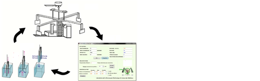
Figure 1. Simplified diagram of the process sol-gel dip coating.
2.2. Characterization
Samples of pure ZnO and ZnO:Sn were characterized. The morphological surface of the films was examined by Scanning Electronic Microscope (SEM) (VEGA3). The structural characterization of the films was analyzed using X-Ray Diffract meter (XRD) (Equinox.3000) Series X-Ray Automatic Diffractometer. The diffractometer reflections were taken at room temperature and the values of 2θ were swapped between 10˚ and 90˚ with Cu Kα1 radiation while the scanning rate was 0.03˚ and the incident wavelength was 1.54056 Å. The optical transmittance measurements of the films were performed with a UV-Visible Spectrophotometer (U-Vis) (Shimadzu 1200) at wavelength range 200 - 900 nm, then the optical band gap energy was calculated with. The valence states of the elements in ZnO and ZnO:Sn were determined by VG Multilab 2000X-Ray Photoelectron Spectroscopy (XPS).
3. Result and Discussion
3.1. Scanning Electron Microscopy (SEM)
Figure 2 shows the images of Scanning Electronique Microscope (SEM) of Undoped ZnO thin film, Sn-doped ZnO thin films 3% and Sn-doped ZnO thin films 5%, respectively in (a), (b) and (c). Interconnected microstructures appeared like-wrinkles form in all samples elaborated and have nearly the same diameter dwrinkle with values between 0.33 µm and 2.33 µm. They seem to be clearer in 3% and 5%. The wrinkles are discontinuouslyconnected and have a direction. Other scientific researchers proposed a link between the size of wrinkles and the percentage of dopant [22] . From SEM micrographs (Figure 2), a visible coalescence is observed, by the forming of interconnected structures containing small crystallites that extend over the entire surface of the layer and which may continue to grow more in the case of doping 3%. These crystallites have almost the same size whatever the composition is between 17 nm and 50 nm.
To better visualize the surface layers and understand how the microstructures are networked and from where they come, wrinkles of (b)-3% were cut in transverse, inclined at 5˚. From the cross-sectional of Figure 3, the surface is uniform, dense and well sintered unlike the volume. The layer is under stress of compressive, such that it compresses and relaxes after. Additionally, increasing the doping rate causes the morphological change of layers that affect on the mechanisms of the nucleation and on wrinkles growth. This instability caused by tin atoms encouraged the growth of network-winkles for destress the layers and reduce the energy of the system. A similar result was found by B. Bahsi et al. [23] in the study of layers of Cu and Mn doped ZnO sol-gel. Furthermore, the surface micrographs clearly showed that the doping displayed an important role for changing and improving the structure of the ZnO films.
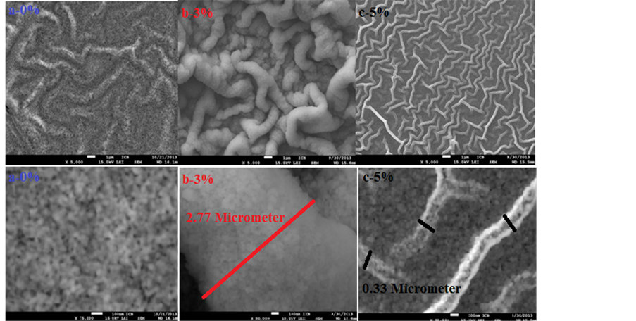
Figure 2. SEM images of Undoped ZnO and Sn-doped ZnO thin films.
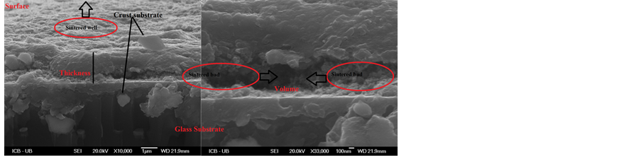
Figure 3. SEM micrographs of Sn-doped ZnO 3% thin film inclined at 5˚ showing the wrinkles cut in transverse.
 (a)
(b)
(c)
(a)
(b)
(c)
Table 1 . (a) Structural parameters of pure ZnO film; (b) Structural parameters of ZnO:Sn 3% film; (c) Structural parameters of ZnO:Sn 5% film.
3.2. X-Ray Diffraction (XRD)
The crystallinity and the preferred crystal orientation of Undoped ZnO and Sn-doped ZnO thin films were analyzed by the X-Ray Diffraction (XRD) method. Figure 4 shows the XRD patterns of pure ZnO and ZnO:Sn thin films. For all samples the peaks position agrees well with the reflections of hexagonal wurtzite type structure of polycrystalline ZnO (JCPDS Card No. 36-1451). No parasitic phase (impurity peak) is observed in the detection limit of the apparatus, which indicate a high purity of the samples. There was no SnO or other phase obtained. Nine major diffraction peaks are seen in all films: (1 0 0), (0 0 2), (1 0 1), (1 0 2), (1 1 0), (1 0 3), (1 1 2), (2 0 1) and (2 0 2) corresponding to planes of Zincite phase. Furthermore, upon increasing the Sn dopant concentration, the intensity of the peaks increases. We observed in all patterns of thin films ZnO a high diffraction intensity for the (101) peak. The lattice spacing was calculated from the Bragg’s formula: [22]
 (1)
(1)
where
 is the lattice spacing,
 the angle of incidence or Bragg diffraction, λ the wavelength
of the radiation and n is the diffraction order (n = 1, 2, ...) The lattice spacing
(d), I/IHigh ratio where I (h k l) is the measured relative intensity
of a plane (h k l), IHigh (h k l) is the highest intensity of the plane
(h k l) taken from the data. Also angle of diffraction (2θ) at the phases identified
along with (h k l) planes of the films are given in Tables
1(a)-(c). The lattice parameters of “a” and “c” were calculated using the
following equation [24] :
the angle of incidence or Bragg diffraction, λ the wavelength
of the radiation and n is the diffraction order (n = 1, 2, ...) The lattice spacing
(d), I/IHigh ratio where I (h k l) is the measured relative intensity
of a plane (h k l), IHigh (h k l) is the highest intensity of the plane
(h k l) taken from the data. Also angle of diffraction (2θ) at the phases identified
along with (h k l) planes of the films are given in Tables
1(a)-(c). The lattice parameters of “a” and “c” were calculated using the
following equation [24] :
 (2)
(2)
From the latest equation, the cell volume is deduced:
 (3)
(3)
The lattice constants “a” and “c” of Undoped and doped ZnO films in Table 2 are in agreement with standard values of (JCPDS Card No. 36-1451), associating the scanning rate. The crystallite size (D) of the films was calculated from the planes of Zincite phase, so as to have information about their crystallinity levels using the well-known Scherrer’s equation [24] :
 (4)
(4)
where D is the crystallite size, K = 0.89, λ = 0.154056 nm the mean wavelength of Cu Kα1 radiation and β the full-width half maximum (FWHM) of Bragg peak observed at Bragg angle θ (rad). The values of D and β obtained are given in Tables 1(a)-(c).
After comparing between ((I/IHigh)*100%) and ((IJCPDS/IHigh JCPDS) *100%), there was not a noted texturing of the layer nor a notable change according to doping, due to their similarity. Furthermore, low doping has not been demonstrated by a modification of the lattice parameters, nor by a displacement of the diffraction peaks, but by an influence on the crystallite size such that Sn low doping ZnO films can reduce the average crystallite size. The crystallite size in agrees with the SEM observation. This observation has an agreement with the literature.
3.3.UV-Visible Spectrophotometer (U-Vis)
The transmittance spectra of Undoped ZnO and Sn-doped ZnO films were measured in the range of 200 - 900 nm as shown in Figure 5, for the longer wavelengths (>380 nm) all the films become transparent. It is found
Table 2. The lattice constants parameters of pure ZnO and ZnO:Sn films.
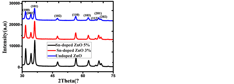
Figure 4. XRD patterns of Undoped ZnO and Sn-doped ZnO thin films.
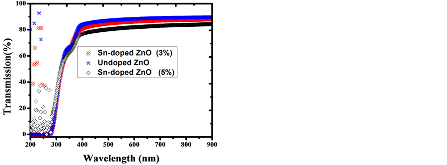
Figure 5. Transmittance spectra of Undoped ZnO and Sndoped ZnO thin films.
that transmittance is over >83% for the visible region. Based on the transmittance spectra in Figure 5, the optical band gap Eg was obtained by extrapolating the linear portion of the plot (αhν)2 versus (hν) to α = 0 according to the following Equation (5):
 (5)
(5)
where hν is the photon energy, Eg is the optical band gap, A is the edge parameter and n = 1/2 for direct gap material. ZnO is one of the most important multifunctional n-type direct band gap semiconductors [25] . The optical band gap Eg of Undoped ZnO and Sn-doped ZnO films are illustrated in Figures 6-8. While Sn doping concentration increases the optical band gap of ZnO films decreases. This shift in the optical band gap may be attributed to the band shrinkage effect because of increasing carrier concentration, Benelmadjat et al. [26] . The values of Eg obtained of ZnO:Sn films are almost the same values obtained by other group of tin doped ZnO films prepared by sol-gel method [27] . The values of the transmissivity and optical band gap are given in Table3
It is also assumed that the absorption coefficient near the band edge shows an exponential dependence on photon energy and this dependence is given as follows [28] [29]
 (6)
(6)
where E is the photon energy, α0 is constant and Eu is the Urbach energy which refers the width of the exponential absorption edge. Inset plots of Figures 6-8 show the variation of (lnα vs. photon energy) for the films. This behavior corresponds primarily to optical transitions between occupied states in the valence band tail to unoccu-
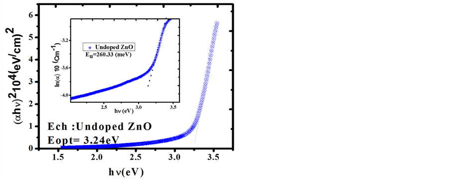
Figure 6. The plots of (αhν)2 versus (hν) and Urbach plots (inset plots) of Undoped ZnO film.
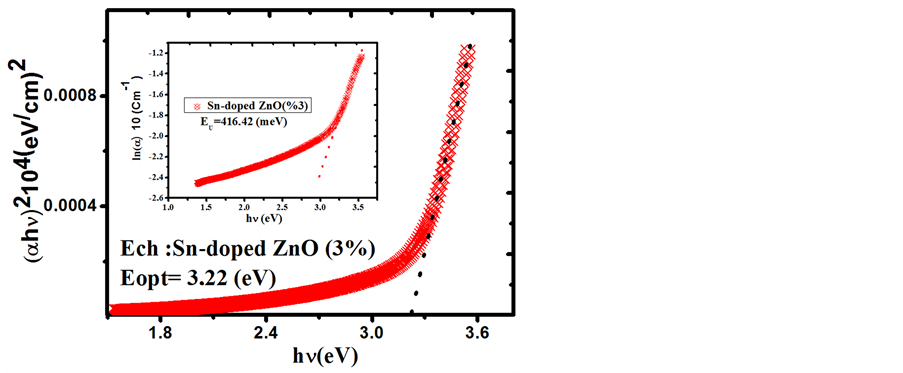
Figure 7. The plots of (αhν)2 versus (hν) and Urbach plots (inset plots) of Sn-doped 3% ZnO film.
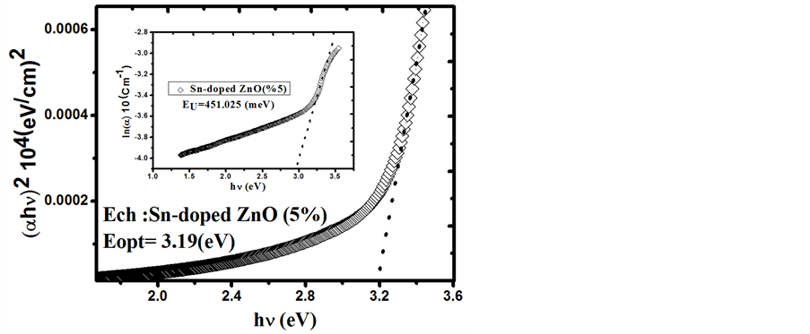
Figure 8. The plots of (αhν)2 versus (hν) and Urbach plots (inset plots) of Sn-doped 5% ZnO film.
Table 3 . Optical parameters of Undoped ZnO and Sn-doped ZnO thin films.
pied states at the conduction band edge. The Eu values were calculated from the slope of Figures 6-8 using relationship:

The values of Eu obtained from this figures are given in Table3 The Eu values change inversely with optical band gaps of the films. The decrease in Eg is attributed to the increase of disorder of the material occurred by doping. This increase leads to a redistribution of states, from band to tail, thus allows for a greater number of possible bands to tail and tail to tail transitions [30] .
3.4. X-Ray Photoelectron Spectroscopy (XPS)
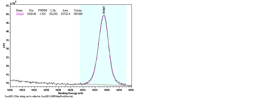
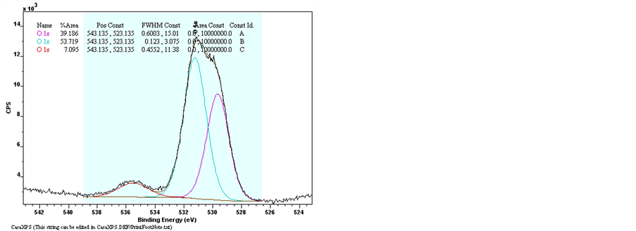
The elements bonding of Undoped Zinc Oxide and Sn-doped Zinc Oxide films were examined by the X-Ray Photoelectron Spectroscopy (XPS). The Figure 9 shows the results of XPS spectra of pure ZnO and ZnO:Sn films with full region scanning from 0 to 1100 eV. The high-resolution scanning information provided in Figure 10 are for separate analysis of the 3 elements: Zn, O, and Sn. Comparing pure ZnO film with ZnO:Sn 5% film; intensity of the major binding energy peaks of doped ZnO has slightly decreased and shifted to lower energy (0.1) eV. The elements of Zn2p, Zn3p, O1s and Sn3d have been detected in the spectrums, and the Auger peaks such as Zn LMM, O KLL and Sn MNN were also observed. Figure 9 shows two strong peaks of pure ZnO film at 1020.7 eV and 1043.9 eV which correspond with Zn2p3/2 and Zn2p1/2, respectively, were shifted at 1020.6 eV
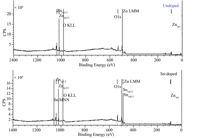
Figure 9. The XPS survey spectrum of pure ZnO and ZnO:Sn thin films.
Zn2p3 3 Zn2p3 3

 O1s 2 O1s 2
 Sn3d5 5
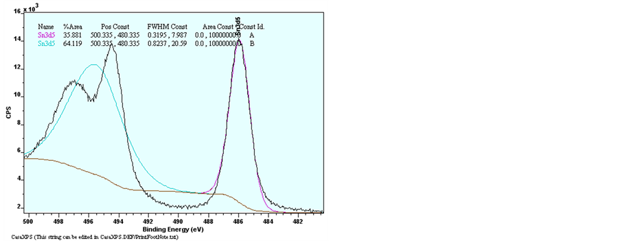
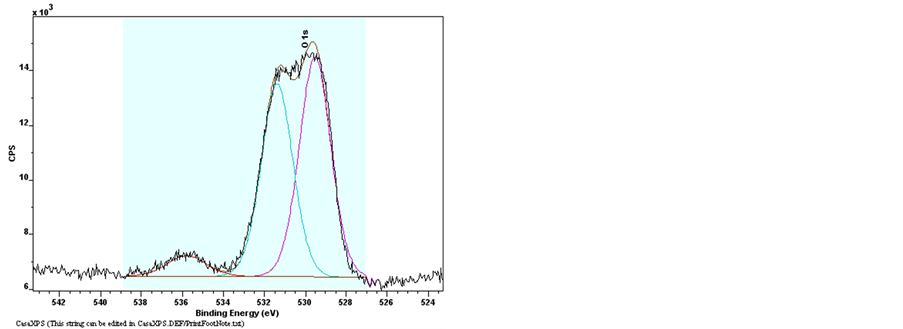
Figure 10. XPS spectra of raw data of Narrow scan O1s, Zn2p3/2, Sn3d3/2 and Sn3d5/2 for pure ZnO and ZnO:Sn thin films.
and 1043.8 eV of ZnO: Sn film [31] . The binding energy of Zn3p3/2 was detected at 88.6 eV of Undoped ZnO and Sn-doped ZnO [32] . This shows that Zn exists only in the oxidized. For ZnO:Sn the O1s peak can be consistently fitted by three components, centered at 530, 531.9 and 536.6 eV. The fitted results indicate that each fitted component has a FWHM less than 2.01 eV. The low binding energy component centered at 530 eV of the O1s spectra is attributed to O2− ions on the wurtzite structure of a hexagonal Zn2+ ion array, surrounded by Zn (or substitutional Sn) atoms, with their full complement of nearest-neighbor O2− ions [33] . The high binding energy component located at 531.9 eV and 536.7 eV is probably attributed to the diatomic anion OH−, or to the either presence of loosely bound oxygen which may be present on the surface of Sn doping ZnO thin films [34] [35] . Sn peaks (Sn3d5/2 and Sn3d3/2) are located at 485.4 eV and 495.1 eV which can be attributed to Sn ions in ZnO:Sn thin film. The appearance of these peaks indicates the incorporation of Sn dopant in the form of O-Sn in ZnO lattice [31] [36] .
This result agrees well with the morphological changes and the shift observed in the optical band gap, as a result no displacement of the diffraction peaks, probably because of scanning rate of 0.03˚. Hence, a high quality of Sn-doped ZnO thin film was obtained by the XPS spectrum.
4. Conclusion
In summary, Undoped Zinc Oxide and Sn-doped Zinc Oxide thin films have been prepared by sol-gel dip-coating technique that helped us to obtain structures with high efficiency. The Scanning Electron Microscopy (SEM) illustrated that the surface morphology of films was affected by the tin doping. The analysis of X-Ray Diffraction (XRD) showed that the structures were hexagonal for all samples and that the Sn low doping ZnO films can reduce the average crystallite size. The transmittance spectra of pure ZnO and ZnO:Sn films have revealed a high visible transmittance over >83%. While the Sn doping concentration was increasing, the optical band gap of ZnO films was decreasing. Furthermore the Urbach energy values change inversely with the optical band gaps of the films. The results of X-Ray Photoelectron Spectroscopy measurement (XPS) confirmed the incorporation of Sn doping in ZnO lattice.
Acknowledgements
This work was supported by all members of “Laboratory of Electronic Microscopy and Materials Science” in University of Science and Technology of Oran and “NanoForm of ICB” University of Bourgogne Dijon France. We would like to thank Mr. Frédéric HERBST for SEM, Mr. Nicolas GEOFFROY for XRD and Olivier HEINTZ for XPS. Also we are grateful to D. Masatomo SUMIYA from “N.I.M.S” Tsukuba, Japan for the correction of XPS spectrum.
References
- Ammaih, Y., Lfakir, A., Hartiti, B., Ridah, A., Thevenin, Ph. and Siadat, M. (2014) Structural, Optical and Electrical Properties of ZnO: Al Thin Films for Optoelectronic Applications. Optical and Quantum Electronics, 46, 229-234. http://dx.doi.org/10.1007/s11082-013-9757-2
- Krajewskia, T.A., Luka, G., Smertenko, P.S., Zakrzewski, A.J., Dybkoa, K., Jakiela, R., Wachnicki, L., Gieraltowska, S., Witkowskia, B.S., Godlewski, M. and Guziewicza, E. (2011) Schottky Junctions Based on The ALD-ZnO Thin Films for Electronic Applications. Acta Physica Polonica A, 120, 19-23.
- Water, W. and Yan, Y.S. (2007) Characteristics of Strontium-Doped ZnO Films on Love Wave Filter Applications. Thin Solid Films, 515, 6992-6996. http://dx.doi.org/10.1016/j.tsf.2007.02.028
- Dubois, M.A. (2003) Thin Film Bulk Acoustic Wave Resonators: A Technology Overview. Memswave, 3, 2-4.
- Park, J.Y., Choi, S.W. and Kim, S.S. (2009) Fabrication of a Highly Sensitive Chemical Sensor Based on ZnO Nanorod Arrays. Nanoscale Research Letters, 5, 353-359. http://dx.doi.org/10.1007/s11671-009-9487-3
- Al-Zaidi, Q.G., Suhail, A.M. and Al-Azawi, W.R. (2011) Palladium-Doped ZnO Thin Film Hydrogen Gas Sensor. Applied Physics Research, 3, 89-99. http://dx.doi.org/10.5539/apr.v3n1p89
- Struk, P., Pustelny, T. and Opilski, Z. (2010) Researches on the Spectral Transmittance of Zinc Oxide ZnO Semiconductor Layers. Acta Physica Polonica A, 118, 1239-1241.
- Shalaka, C., Navale, A.B. and Mulla, I.S. (2009) Photoluminescence and Gas Sensing Study of Nanostructured Pure and Sn Doped ZnO. Materials Science and Engineering C, 29, 1317-1320.http://dx.doi.org/10.1016/j.msec.2008.09.050
- Lijun, L., Ke, Y., Yang, W. and Ziqiang, Z. (2010) Photoluminescence and Field Emission Properties of Sn-Doped ZnO Microrods. Applied Surface Science, 256, 3361-3364. http://dx.doi.org/10.1016/j.apsusc.2009.12.034
- Norton, D.P., Overberg, M.E., Pearton, S.J., Pruessner, K., Budai, J.D., Boatner, L.A., Chisholm, M.F., Lee, J.S., Khim, Z.G., Park, Y.D. and Wilson, R.G. (2003) Origin of Ferromagnetism in Multilayers: Diluted Magnetic Semiconductor or Clustering Effect? Applied Physics Letters, 83, 5488. http://dx.doi.org/10.1063/1.1637719
- Rensmo, H., Keis, H., Lindstrom, K., Sodergren, S., Solbr, A., Hagfeldt, A. and Lindquist, S.E. (1997) High Light-to-Energy Conversion Efficiencies for Solar Cells Based on Nanostructured ZnO Electrodes. The Journal of Physical Chemistry B, 101, 2598-2601. http://dx.doi.org/10.1021/jp962918b
- Meng, Y., Lin, Y. and Yang, J. (2013) Synthesis of Rod-Cluster ZnO Nanostructures and Their Application to Dye-Sensitized Solar Cells. Applied Surface Science, 268, 561-565. http://dx.doi.org/10.1016/j.apsusc.2012.12.171
- Alhamed, M. and Abdullah, W. (2013) Structural and Optical Properties of Cu2ZnSnO4 Thin Film Prepared by Dip-Coating Sol-Gel. Journal of Electron Devices, 18, 1563-1567.
- Thongsuriwong, K., Amornpitoksuk, P. and Suwanboon, S. (2013) Structure, Morphology, Photo-catalytic and Anti-bacterial Activities of ZnO Thin Films Prepared by Sol-Gel Dip-Coating Method. Advanced Powder Technology, 24, 275-280. http://dx.doi.org/10.1016/j.apt.2012.07.002
- Tari, O., Aronne, A., Addonizio, M.L., Daliento, S., Fanelli, E. and Pernice, P. (2012) Sol Gel Synthesis of ZnO Transparent and Conductive Films: A Critical Approach. Solar Energy Materials & Solar Cells, 105, 179-186.http://dx.doi.org/10.1016/j.solmat.2012.06.016
- Znaidi, L., Touam, T., Vrel, D., Souded, N., Yahia, S.B., Brinza, O., Fischer, A. and Boudrioua, A. (2013) AZO Thin Films by Sol-Gel Process for Integrated Optics. Coatings, 3, 126-139. http://dx.doi.org/10.3390/coatings3030126
- Kondratiev, V.I., Kink, I. and Romanov, A.E. (2013) Low Temperature Sol-Gel Technique For Processing Al-Doped Zinc Oxide Films. Materials Physics and Mechanics, 17, 38-46.
- Musat, V., Mazilu, M., Diaconu, I.B. and Balta, S. (2009) Sol-Gel Preparation of Semiconductive Oxides 1-D Nano-structures on Glass Substrate. Ovidius University Annals of Chemistry, 20, 119-121.
- Kaneva, N.V. and Dushkin, C.D. (2011) Preparation of Nanocrystalline Thin Films of ZnO by Sol-Gel Dip Coating. Journal of the Chemicals Institutes of the Bulgarian Academy of Sciences and of the Union of Chemists in Bulgaria, 43, 259-263.
- Gan, X.Y., Li, X.M., Gao, X.D., Zhuge, F.W. and Yu, W.D. (2010) ZnO Nanowire and TiO2 Nanoparticle Photoanodes Prepared by the Ultrasonic Irradiation Assisted Dip Coating Method. Thin Solid Films, 518, 4809-4812.http://dx.doi.org/10.1016/j.tsf.2010.01.043
- Chen, K.J., Hung, F.Y., Chen, Y.T., Chang, S.J. and Hu, Z.S. (2010) Surface Characteristics, Optical and Electrical Properties on Sol-Gel Synthesized Sn-Doped ZnO Thin Film. Materials Transactions, 51, 1340-1345.http://dx.doi.org/10.2320/matertrans.M2009378
- Ilican, S., Caglar, M. and Caglar, Y. (2010) Sn Doping Effects on the Electro-Optical Properties of Sol Gel Derived Transparent ZnO Films. Applied Surface Science, 256, 7204-7210. http://dx.doi.org/10.1016/j.apsusc.2010.05.052
- Banu, B.Z. and Yavuz, O.A. (2007) Effects of Mn and Cu Doping on the Microstructures and Optical Properties of Sol-Gel Derived ZnO Thin Films. Optical Materials, 29, 672-678. http://dx.doi.org/10.1016/j.optmat.2005.11.016
- Prabhu, Y.T., Venkateswara, R.K., Sesha, S.K.V. and Siva, K.B. (2013) X-Ray Analysis of Fe Doped ZnO Nanoparticles by Williamson-Hall and Size-Strain Plot. International Journal of Engineering and Advanced Technology (IJEAT), 2, 268-274.
- Wanga, J., Elamurugua, E., Sallet, V., Jomard, F., Lusson, A., Botelho do Regoc, A.M., Barquinha, P., Gonc, G., Martins, R. and Fortunato, E. (2008) Effect of Annealing on the Properties of N-Doped ZnO Films Deposited by RF Magnetron Sputtering. Applied Surface Science, 254, 7178-7182. http://dx.doi.org/10.1016/j.apsusc.2008.05.321
- Benelmadjat, H., Boudine, B., Halimi, O. and Sebais, M. (2009) Photo Response and H2 Gas Sensing Properties of Highly Oriented Al and Al/Sb Doped ZnO Thin Films. Optics & Laser Technology, 41, 630-633.http://dx.doi.org/10.1016/j.optlastec.2008.09.011
- Aksoy, S., Caglar, Y., Ilican, S. and Caglar, M. (2010) Effect of Sn Dopants on the Optical and Electrical Properties of ZnO Films. Optica Applicata, XL, 7-14.
- Urbach, F. (1953) The Long-Wavelength Edge of Photographic Sensitivity and of the Electronic Absorption of Solids. Physical Review, 92, 1324. http://dx.doi.org/10.1103/PhysRev.92.1324
- Chahmat, N., Haddad, A., Ain-Souya, A., Ganfoudi, R., Attaf, N., Aida, M.S. and Ghers, M. (2012) Effect of Sn Doping on the Properties of ZnO Thin Films Prepared by Spray Pyrolysis. Journal of Modern Physics, 3, 1781-1785.http://dx.doi.org/10.4236/jmp.2012.311222
- O’Leary, S.K. (1998) Optical Absorption, Disorder, and the Disorder Less Limit in Amorphous Semiconductors. Applied Physics Letters, 72, 1332. http://dx.doi.org/10.1063/1.120985
- Sherwood, P.M.A., Briggs, D. and Seah, M.P. (1983) Practical Surface Analysis by Auger and X-Ray Photoelectron Spectroscopy. Wiley, New York.
- Haemers, G., Verbist, J.J. and Maroie, S. (1984) Surface Oxidation of Polycrystalline “Alpha” (75% Cu et 25% Zn) and “Beta” (53% Cu et 47% Zn) Brass as Studied by XPS: Influence of Oxygen Pressure. Applications of Surface Science, 17, 463-476. http://dx.doi.org/10.1016/0378-5963(84)90006-0
- Clakes-Olsson, O.A. and Hornstrom, S.E. (1994) An AES and XPS Study of the High Alloy Austenic Stainless Steel 254 SMO Tested in a Ferric Chloride Solution. Corrosion Science, 36, 141-151.http://dx.doi.org/10.1016/0010-938X(94)90115-5
- Atrens, A. and Lim, A.S. (1990) ESCA Studies of Nitrogen-Containing Stainless Steels. Applied Physics A, 51, 411-418. http://dx.doi.org/10.1007/BF00348382
- Mustin, C., De Donato, Ph., Benoit, R. and Erre R (1993) Spatial Distribution of Iron and Sulphure Species on the Surface of Pyrite. Applied Surface Science, 68, 147-158.
- Tateishi, T., Ito, Y. and Okazaki, Y. (1997) Corrosion Resistance of Implant Alloys in Pseudo Physiological Solution and Role of Alloying Elements in Passive Film. Materials Transactions, 38, 78-84.http://dx.doi.org/10.2320/matertrans1989.38.78
NOTES

*Corresponding author.