Advances in Materials Physics and Chemistry
Vol.3 No.5(2013), Article ID:36471,6 pages DOI:10.4236/ampc.2013.35036
Bi-Directional Giant Magneto Impedance Sensor
Oregon Episcopal School High School, Portland, USA
Email: uppilih@go.oes.edu
Copyright © 2013 Harsha Uppili, Bevin Daglen. This is an open access article distributed under the Creative Commons Attribution License, which permits unrestricted use, distribution, and reproduction in any medium, provided the original work is properly cited.
Received June 18, 2013; revised July 20, 2013; accepted August 1, 2013
Keywords: Giant Magneto Impedance; Bi-Directional Sensor; Permalloy
ABSTRACT
A thin film giant magneto impedance (GMI) based on magnetic field sensor has been developed using electrodeposited Ni-Fe permalloy. Chemical composition, surface morphology, and magnetic properties of Ni-Fe permalloy were characterized as a function of plateup parameters, and process conditions were established to deposit a Ni-Fe thin film with a high permeability (~1000) and a low coercivity (0.6 Oersted). Conventional GMI sensors are uni-directional and are several millimeters long. In this work, a spiral-shaped sensor using electroplated Ni-Fe permalloy to detect bi-directional magnetic field is reported. Excellent bi-directional magnetic field sensing has been demonstrated using the 1 mm2 compact double-spiral structure.
1. Introduction
The giant magneto impedance (GMI) effect consists of a large change in AC complex impedance in soft magnetic materials, and is in the presence of an applied DC magnetic field. The GMI effect in Co-based amorphous wires was first reported by Panina and Mohri in 1994 [1]. GMI sensors have received widespread attention due to the applicability of sensing low magnetic fields near pico Tesla values [2]. Since the first publication of the GMI effect, several groups have focused on improving both the sensitivity and the dimensionality of the sensors [3-9]. Ferromagnetic soft glass-coated magnetic wires are widely used in the fabrication of GMI sensors since the cylindrical shape results in a large GMI effect [8,9]. However, GMI sensors in modern consumer devices require the development of thin film miniature GMI sensors compatible with semiconductor electronics. An emphasis has been placed on improving the sensitivity of the thin film GMI sensors by creating an alternating stack of ferromagnetic film and a non-magnetic conductor such as copper [10-14]. Such stacks exhibit high values of transverse and longitudinal magneto impedance with longitudinal anisotropy [12]. The formation of thin film stacks requires vacuum processing for precise thickness and interface control. Electro-deposition of Ni-Fe permalloy offers an attractive low-cost alternative approach for fabrication of GMI sensors [15]. A high quality soft magnetic permalloy with high permeability and low coercivity was reported for electro-deposited thin and thick film [16]. This work reports GMI sensors fabricated using a selective electro-deposition technique. Conventional GMI sensors are uni-directional and are several millimeters long to achieve the necessary sensitivity [15]. Atortuous shape of GMI sensor using magnetic ribbon was reported [17] with the length along with one axis significantly longer than the normal axis. Such a layout creates a compact sensor element but still the detection is primarily unidirectional. In this work, a simple, low cost GMI sensor has been reported with bidirectional sensitivity.
2. Principle of the GMI Sensor
When a soft ferromagnetic material (low coercivity, HC and high Permeability, μ) is subjected to a high frequency alternating current and an applied magnetic field, a large change in the skin depth is achieved, also causing a dramatic change in impedance (Z, AC resistance). This is known as the “Giant Magneto Impedance” (GMI) effect, pictorially illustrated in Figure 1 [18] and graphically shown in Figure 2.
The skin effect (or skin depth) occurs when an alternating current (AC) applied to a conductive material flows along the skin of the conductor. High AC frequencies create a changing magnetic field that in turn creates an electric field. The electric field opposes change in current density. Most of the opposition to current flow occurs in the core of the conductor, forcing current to flow in the outer “skin” of the conductor.
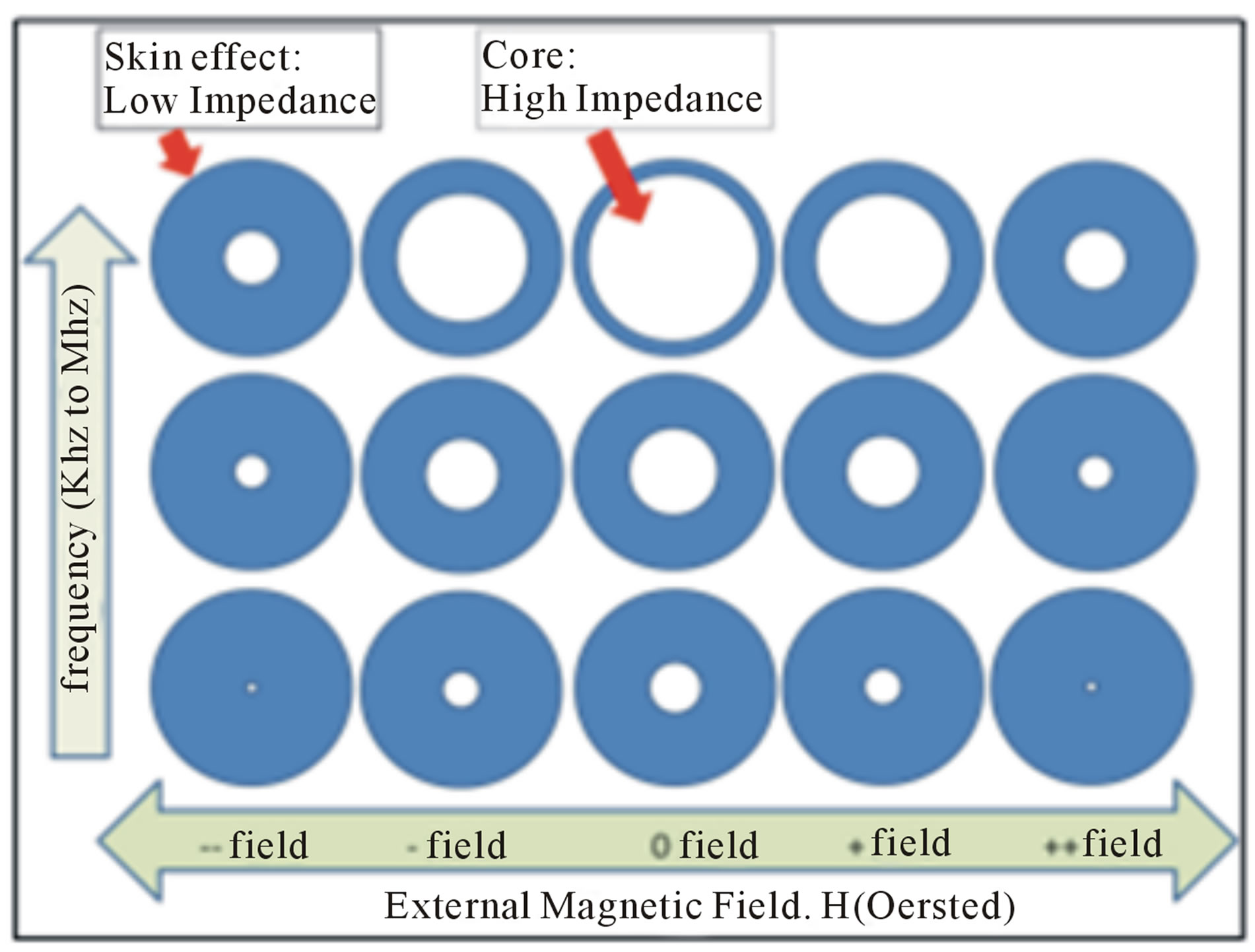
Figure 1. Skin effect (or Skin depth) illustration.
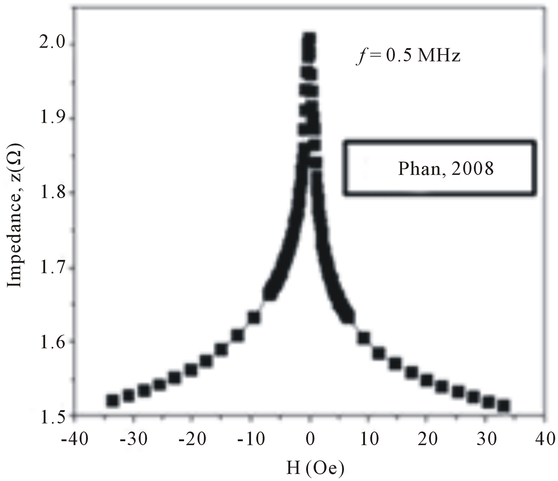
Figure 2. GMI - Skin effect impact on impedance.
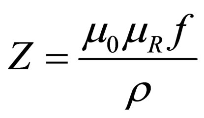
Impedance is proportional to the skin depth
 (1)
(1)
where  is the skin depth.
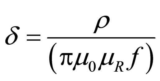 (2)
(2)
where 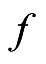 is the frequency of the AC current,
 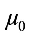 is the permeability of free space,
 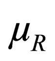 is the relative permeability, and
  is the resistivity of the material.
Therefore, Impedance
 (3)
(3)
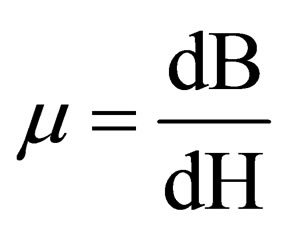
Relative permeability (µR) is a measure of the ease with which a specimen can be magnetized. A high relative permeability increases impedance sensitivity to the frequency of AC current. Coercivity (HC) is the extent of reverse magnetization required to bring an induced magnetism to zero. Materials with very low coercivity show high magnetic sensitivity.
Permeability is the slope of the B-H loop at low field
 (4)
(4)
In ideal soft magnetic materials, permeability peaks at zero external field and drops precipitously in the presence of a magnetic field. This principle is used in a GMI sensor, where on application of a magnetic field, impedance “Z” can change drastically as per Equation (3) [18].
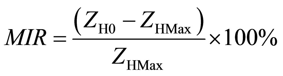
Magneto Impedance Ratio is defined as:
 (5)
(5)
where ZH0 is the measured impedance in the absence of any external magnetic field and ZHMax is the measured impedance in the presence of magnetic field.
Impedance Z = R + jωL (6)
where R = Resistance, L= Inductance, ω = angular frequency, and ωL = X = Reactance. Magneto Impedance Ratio (MIR), Magneto Resistance Ratio (MRR), and Magneto Reactance Ratio (MXR) [19,20] can each be utilized to produce a Giant Magneto Sensor.
3. Structure of GMI Sensor
Typical magnetic sensors involve three uni-axial elements to sense tri-axial magnetic fields (Figure 3) [15, 21]. However, a single sensor that can measure magnetic fields in both X and Y directions simultaneously could provide greater versatility. Such sensors can be formed by using a spiral-shaped structure (Figure 3). A spiral shaped sensor structure also could have very small formfactor for easy integration in an integrated circuit. In this paper, spiral shaped GMI sensors have been fabricated and reported for the first time.
Figure 4 shows a picture of a double spiral GMI sensor fabricated on a silicon substrate.
4. Sensor Fabrication
The sensor was fabricated using thin film etching tech-
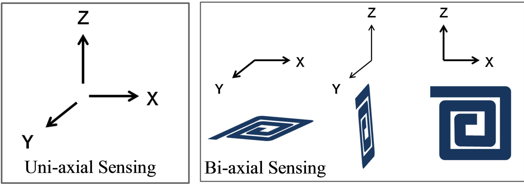
Figure 3. Uni-axial and bi-axial magnetic sensor configurations.
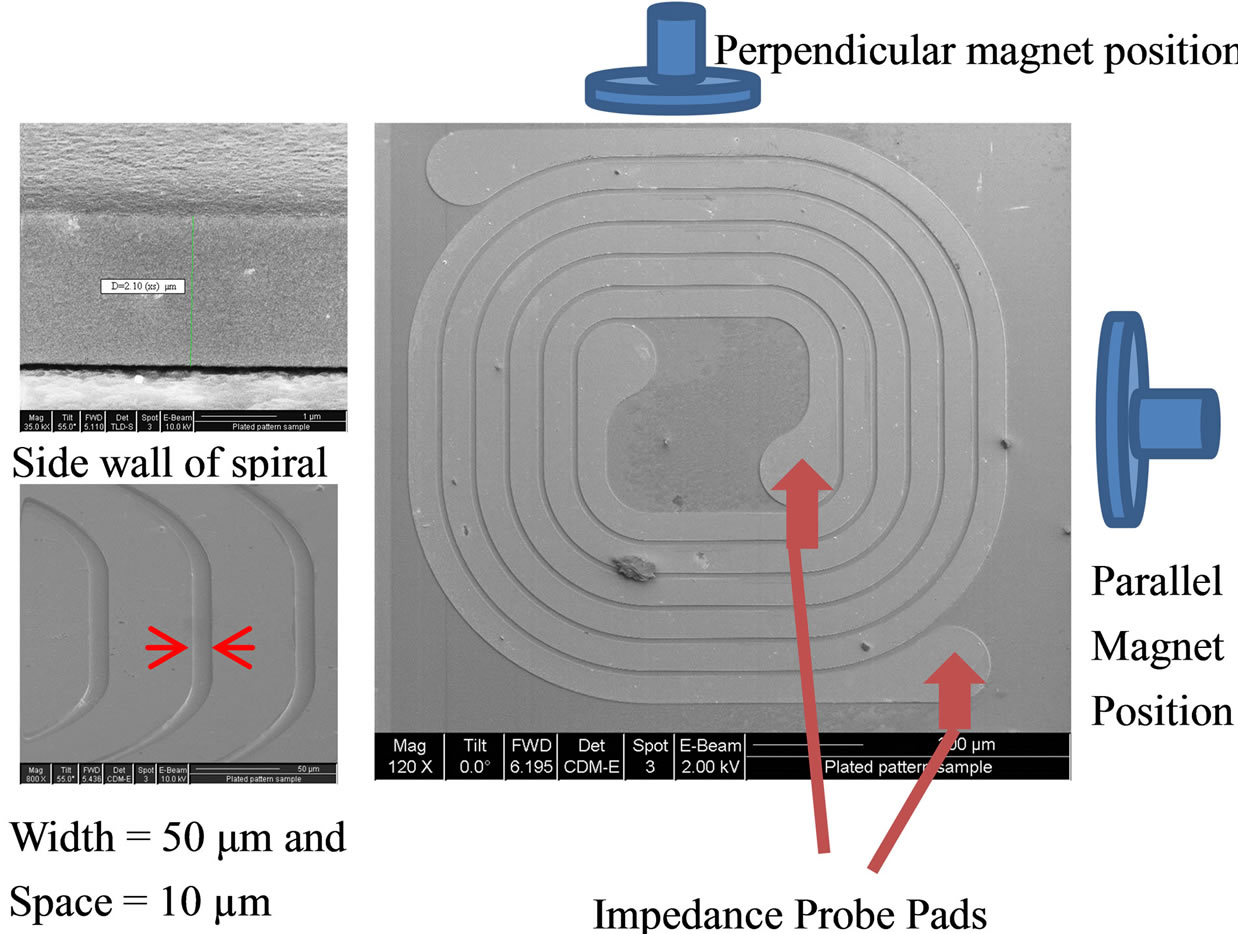
Figure 4. Bi-directional spiral GMI sensor structure.
niques on an oxidized silicon wafer. The development of the sensor material, a critical part of the fabrication process, is described below.
Sensor Material Deposition
The sensor material was a thin film Fe-Ni alloy deposited using an electroplating approach [16]. Nickel sulfate, iron sulfate, boric acid, sodium saccharine, and sodium lauryl sulfate, at pre-determined quantities, were mixed with 150 mL of de-ionized water to form the electroplating bath (Table 1). A small piece of a silicon substrate, with 1000 Ǻ Silicon oxide and a thin seed layer (250 Ǻ) of copper, was used as the cathode. A pure strip of Nickel served as the anode. Electrodes were placed in a beaker and connected to a DC power supply. An electrical vibrating agitator was used to provide mixing.
Minimizing oxygen contamination of the electroplating chemicals was a crucial part of the fabrication process. First, DI water was deoxygenated by bubbling nitrogen before chemicals were added. A blanket of Nitrogen was maintained on top of the plating solution. After the completion of plating, sample roughness was analyzed under an optical microscope and the chemical composition was analyzed using Energy Dispersive X-ray (EDX) in a Scanning Electron Microscope (SEM). The molar ratio of Ni to Fe in the chemical bath was varied during experimentation based on the EDX results in order to achieve Fe20Ni80 ratio in the thin film. The samples were measured for Coercivity and permeability using a B-H looper. To fabricate the sensor, Si/SiO2 wafer with 200 Å Cu seed layer was first pre-patterned with photo-resist template. The Fe20Ni80 thin films were then electroplatedon pre-patterned samples. After the completion of electroplating, photoresist was stripped in acetone. The Cu seed layer from the field region was etched off selectively in a bath of 10% acetic acid +10% hydrogen peroxide + water for 3 minutes. This step completed the fabrication of the sensor (Figure 5).
5. Analysis and Discussion
5.1. Fe-Ni Thin Film Growth and Characterization
Electroplating of Fe-Ni was first investigated on un-patterned Si/SiO2/Cu samples. Several experimental plateup variables affect the characteristics of Fe-Ni alloy. For
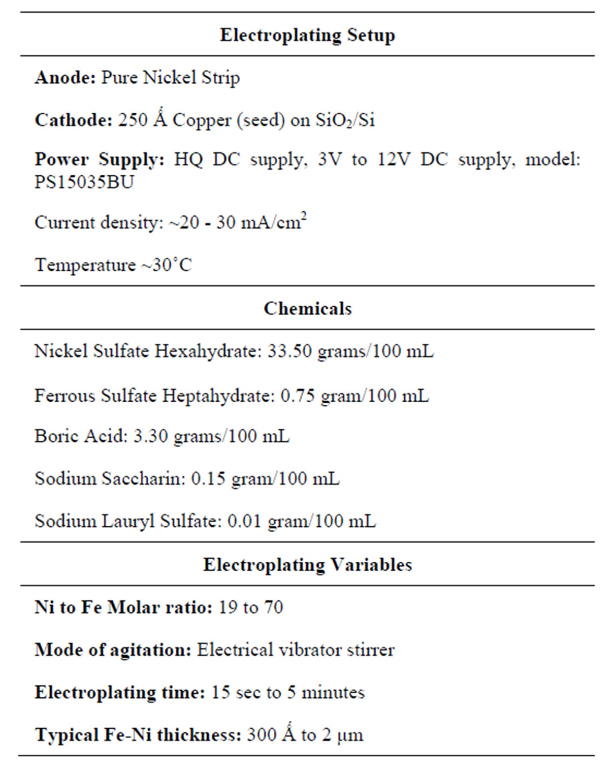
Table 1. Electroplating Details.
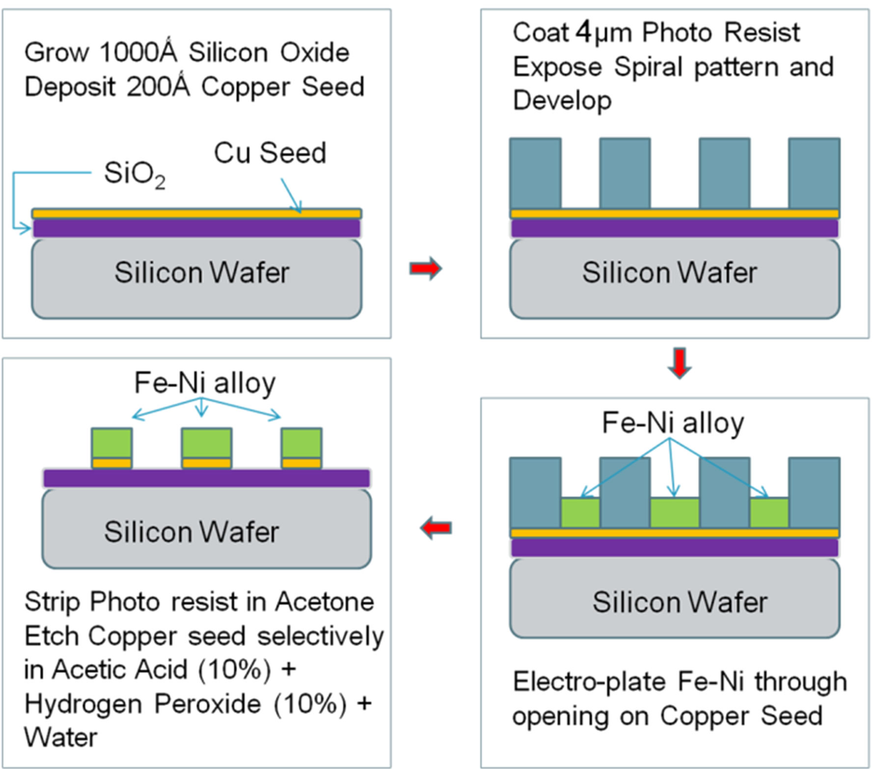
Figure 5. Spiral sensor process flow.
example, the morphology and surface roughness of Fe-Ni alloy is highly dependent on the degree agitation of the plating solution. A plot of the concentration of Fe in the Fe-Ni alloy shows an inverse linear dependence on the molar ratio of Ni to Fe in the electro-plating solution (Figure 6).
The electroplating rate was determined to be ~1 µm/ minute based on the SEM cross-section analysis. A strong coercivity dependence on the sample thickness was observed (Figure 7). Coercivity improved to lower values for thicker Fe-Ni film. Although the reason for such behavior is not clear, it is hypothesized that the improved coercivity is due to thicker samples having a greater magnetization moment available for measurement. A sample with the best soft magnetic property showed coercivity of 0.60 Oersted and relative permeability of 1000 (Figure 8).
5.2. Magneto Impedance Characterization of Sensor
The magneto-impedance behavior of the patterned Fe20Ni80 thin film sensor was characterized in detail. AC Impedance of the sensor samples was measured at frequencies ranging from 30 KHz to 2 GHz in steps of 1.25 MHz. The high-frequency measurement unit was calibrated by measuring the impedance with the probes 1) not in contact with any metal (open), 2) shorted using highly conductive material (shorts), and 3) connected to 50 Ω load resistor. A permanent magnet was positioned at distances varying from 0.5 cm to 10 cm away from the sample to study the sensitivity of the alloy to an external magnetic field. Magnetic field strength as a function of distance was determined using a Gauss meter.
Below 10 MHz, impedance was found to be insensitive to the external magnetic field. Measured resistivity of the spiral sensor, ρ, was found to be 17.9 µΩ-cm. The
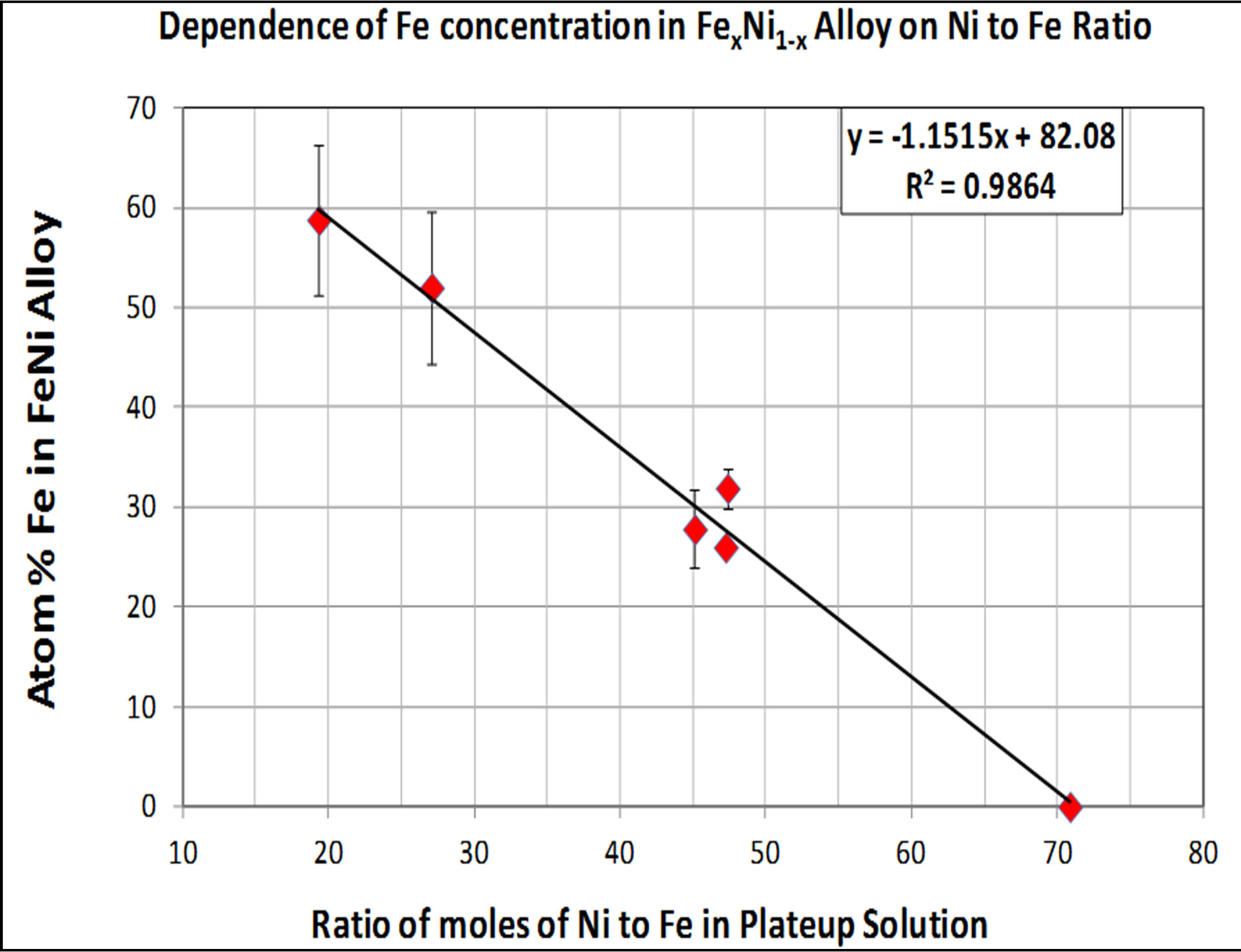
Figure 6. Dependence of Fe concentration in Fe-Ni film on Ni to Fe molar ratio (EDX measurement).
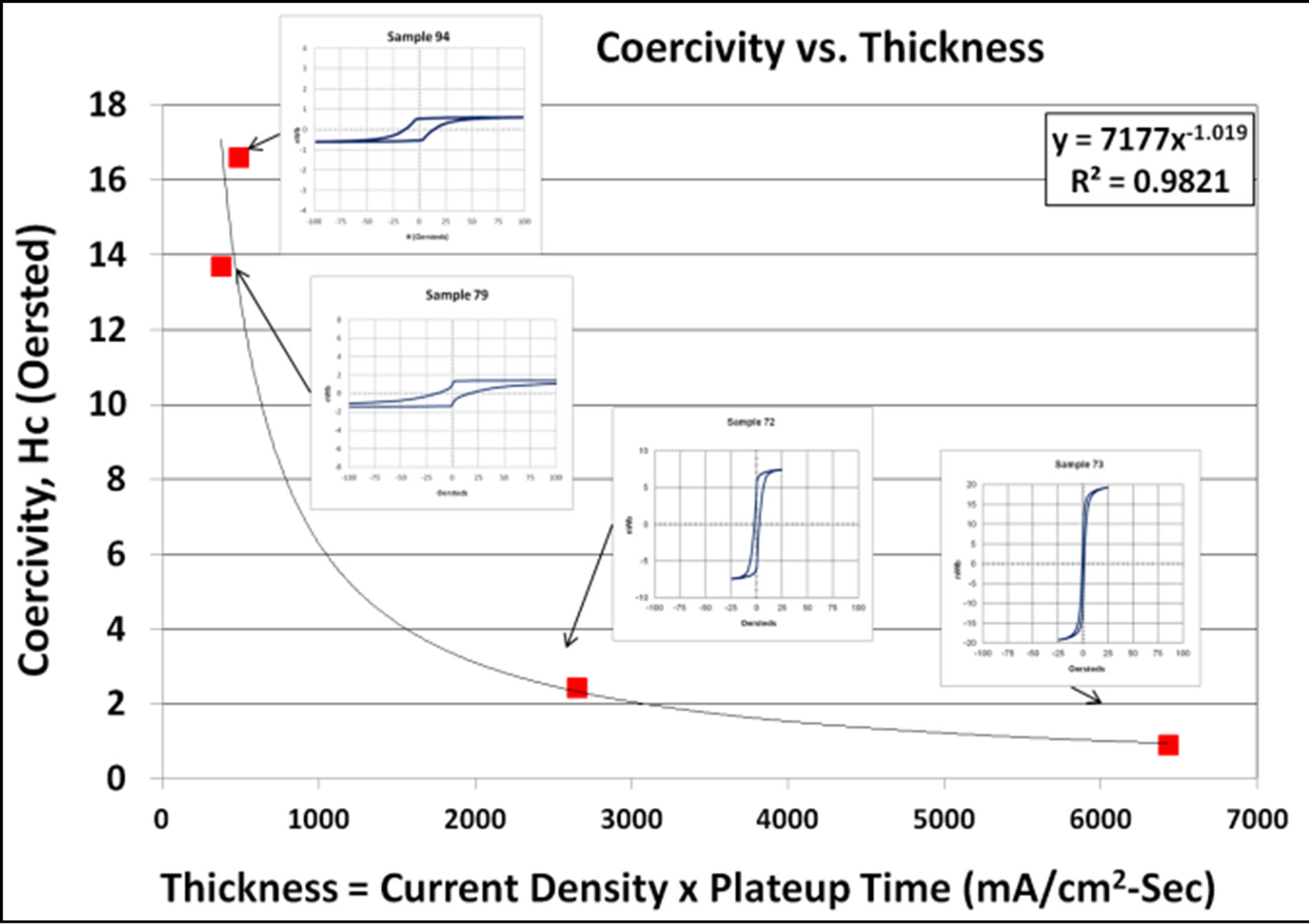
Figure 7. Coercivity dependence on Ni-Fe film thickness.
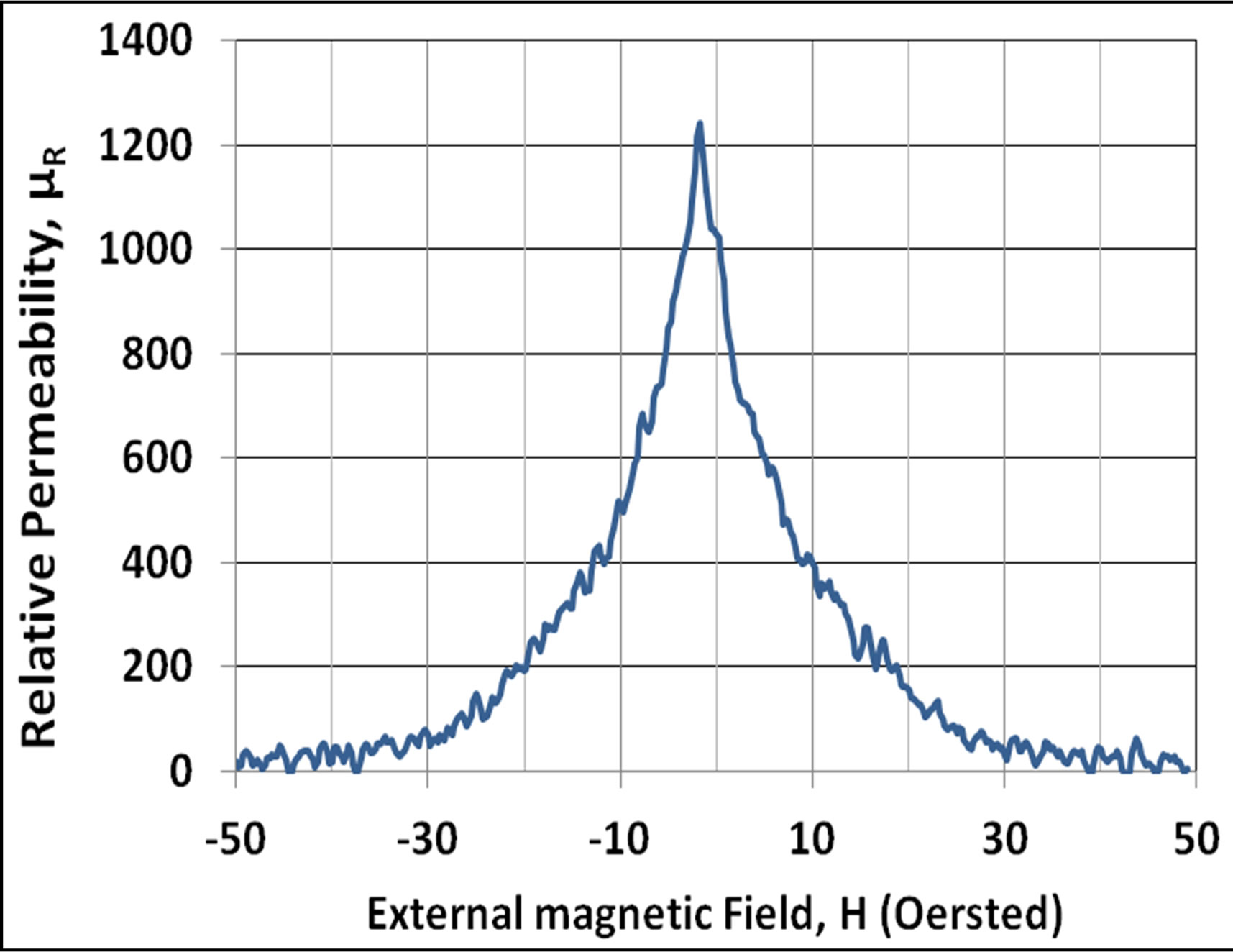
Figure 8. Permeability drop in external magnetic field.
calculated skin depth of ~0.97 µm at ƒ = 40MHz was less than half the thickness of the sample (1.05 µm). Therefore, it is expected that skin effect would start to significantly impact impedance at frequencies ≥ 40 MHz. Between 10 MHz and 1 GHz, the GMI effect was observed where the impedance changed rapidly in the presence of an external magnetic field due to large changes in the skin depth induced by a large drop in relative permeability (Figure 9, Equation (4)).
At frequencies above 1 GHz, impedance was insensitive to the external magnetic field due to the eddy current dampening of magnetic domain walls (Figure 10).
The bi-directional sensing of magnetic field using a single sensor was tested by holding the magnet parallel and perpendicular to the sensor during impedance measurements (Figure 9).
For both parallel and perpendicular magnet orientations, comparable Magneto Impedance Ratio vs. frequency behavior demonstrates bi-directional sensing. It is important to note that the MIR results from this study are nearly 5 times higher than the previously highest published result for electroplated thin film [15]. In addition, the MIR results are as high as the reported values for a significantly more complicated multi-layered structured [14]. Both MIR and MRR have sensitivity of ~0.2%/ Gauss at low magnetic fields. This drops to ~0.01%/ Gauss at B > 1000 Gauss. Magneto Reactance Ratio (MXR) shows the largest sensitivity to external magnetic field. MXR has good low-field sensitivity (2%/Gauss) for B ~ 3 Gauss, ƒ ~ 300 - 500 MHz (Figure 11). MXR also has improved high-field sensitivity (0.26%/Gauss) for B > 1000 Gauss, ƒ < 5 MHz (Figure 12).
When an AC current flows through a spiral coil structure, magnetization created in the metal lines interact causing large change in inductance, L and hence reactance, X (X = ωL) values. This could explain the reason for the large Magneto Reactance Ratio sensitivity compared to Magneto Resistance and Magneto Impedance Ratios. It is possible to use MXR in conjunction with MIR and MRR results to produce a sensor with very wide magnetic field sensitivity. Between measurements under varying magnetic fields, consistent impedance measurement results were observed for data taken at zero magnetic field demonstrating the low coercivity of the Fe-Ni thin film.
Figure 9. Bi-directional sensing in spiral sensor.
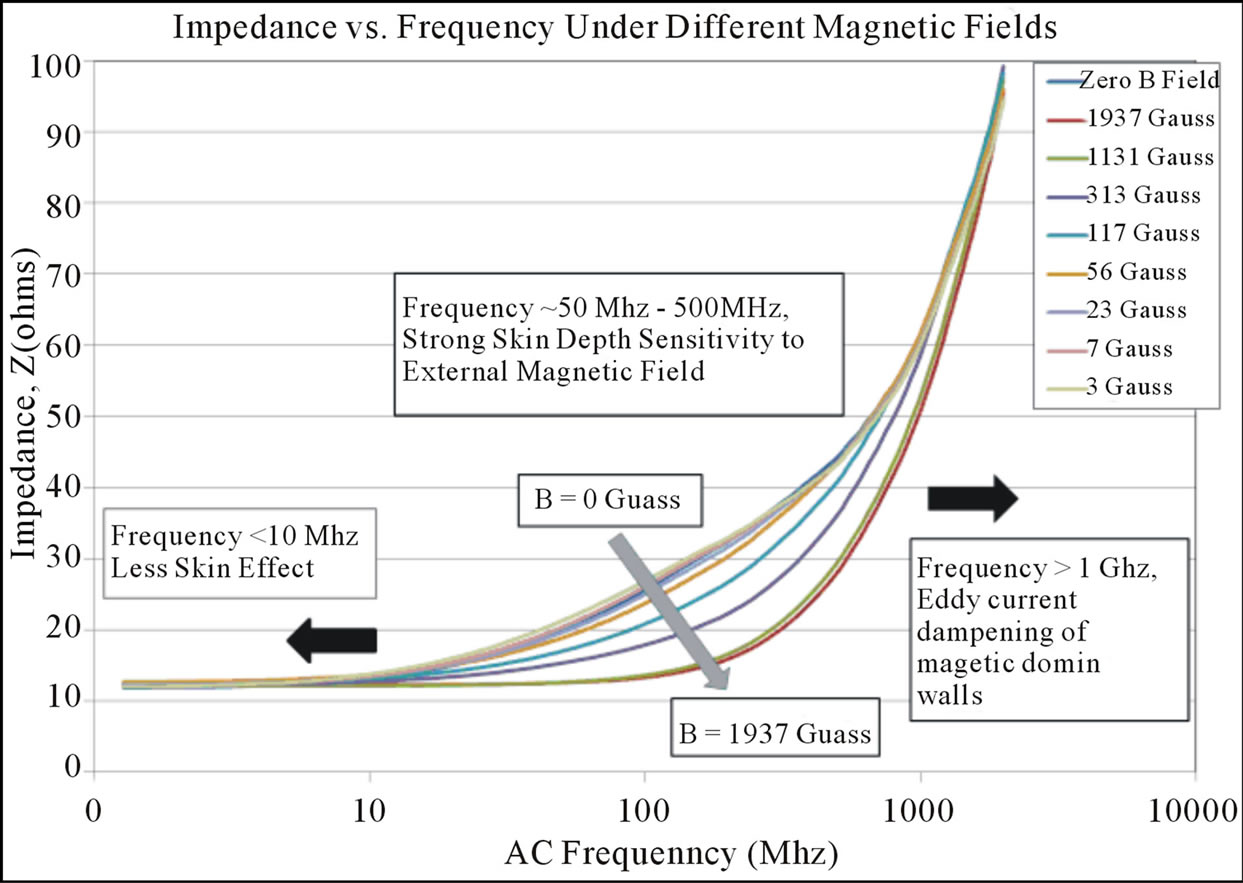
Figure 10. GMI effect as a function of measurement frequency and applied magnetic field.
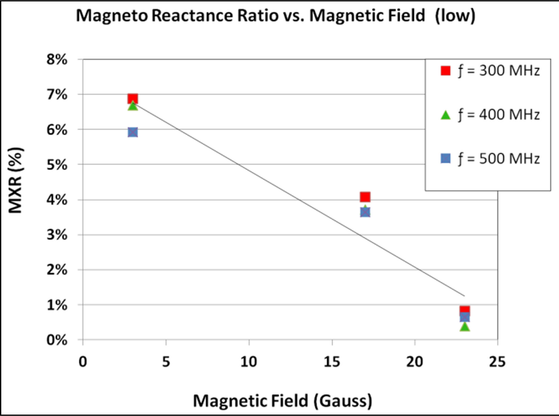
Figure 11. Spiral sensor Magneto Reactance at low field.
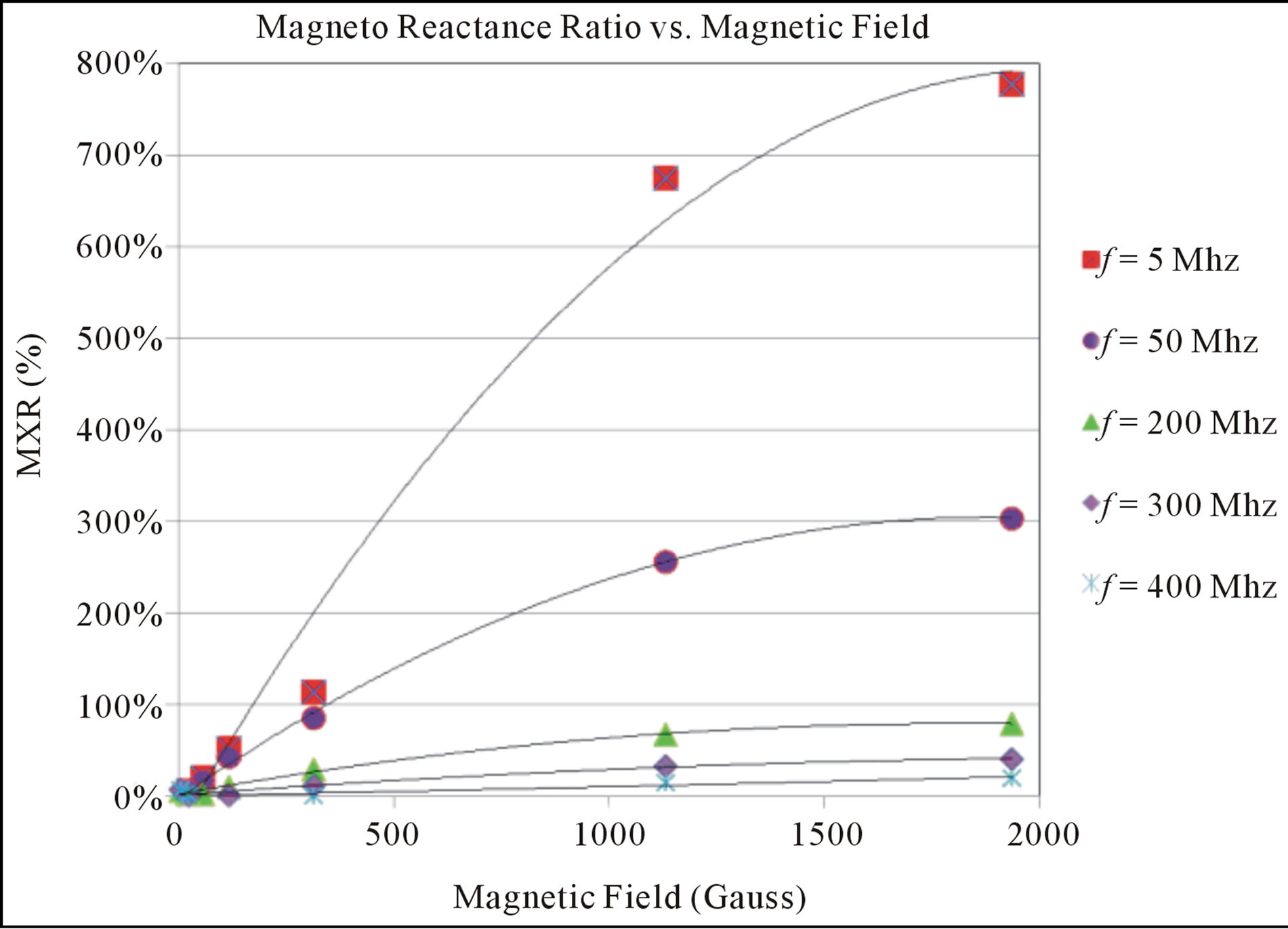
Figure 12. Spiral sensor Magneto Reactance at high field.
6. Conclusion
This work has demonstrated the first ever bi-directional magnetic field sensor based on the GMI effect, using dual spiral shaped sensor element. A spiral shaped structure shows high Giant Magneto Reactance sensitivity due to a large contribution from the change in inductance values. The bi-directional, GMI-based magnetic sensor demonstrates high sensitivity to a wide range of external magnetic fields (3 Gauss to 2000 Gauss). There are civilian and military applications that require overall magnetic sensing and not individual X/Y sensing. The proposed spiral-shaped sensor provides great versatility to sense the overall magnetic field. The spiral structure provides the best alternate approach to sensing X and Y fields since it is much more compact than long metal lines typically used in uniaxial GMI sensors, which are typically 2 mm to 3 mm long. The spiral structure also shows double signal sensitivity as compared with long metal lines. The sensor has a small form-factor of 1 mm2, enabling easy integration and low power consumption. Such sensors may be formed on top of an ASIC circuit which could be used to measure high frequency GMI signals. Future work includes studying systematically the increase in magnetic field sensitivity of the spiral structures over linear structures and developing a theoretical model to explain the observed Magneto Reactance (MXR) behavior as a function of frequency and external magnetic field strength. This is important to create bi-directional high sensitivity, wide field magnetic sensors. We will also investigate methods to further improve coercivity and relative permeability of electroplated Fe-Ni alloys, Literature [12-14], shows that a stack consisting of alternating layers of Fe-Ni and Copper has MIR sensitivity as high as 40%/Oersted. Our goal is to develop an electroplated spiral MIR sensor that has alternating layers to Fe-Ni and Copper.
7. Acknowledgements
I would like to thank Dr. Steve Decker of Oregon Episcopal School’s Science Department. I would also like to thank Dr. Ed Godshalk for his assistance with AC probe measurements.
REFERENCES
- L. V. Panina and K. Mohri, “Magneto-Impedance Effect in Amorphous Wires,” Applied Physics Letters, Vol. 65, No. 9, 1994, pp. 1189-1191. doi:10.1063/1.112104
- K. Mohri, “Magneto-Impedance Sensor,” Nagoya University, Nagoya.
- D. C. Jiles, “Recent Advances and Future Directions in Magnetic Materials,” Acta Materialia, Vol. 51, No. 19, 2003, pp. 5907-5939. doi:10.1016/j.actamat.2003.08.011
- N. Laurita, A. Chaturvedi, C. Bauer, P. Jayathilaka, A. Leary, C. Miller, M.-H. Phan, M. E. McHenry and H. Srikanth, “Enhanced Giant Magnetoimpedance Effect and Field Sensitivity in Co-Coated Soft Ferromagnetic Amorphous Ribbons,” Journal of Applied Physics, Vol. 109, No. 7, 2011, Article ID: 07C706.
- V. Zhukova, M. Ipatov and A. Zhukov, “Thin Magnetically Soft Wires for Magnetic Microsensors,” Sensors, Vol. 9, No. 11, 2009, pp. 9216-9240. doi:10.3390/s91109216
- A. F. Cobeño, A. Zhukov, J. M. Blanco and J. Gonzalez, “Giant Magnetoimpedance Effect in CoMnSiB Amorphous Microwires,” Journal of Magnetism and Magnetic Materials, Vol. 234, No. 3, 2001, pp. 359-365. doi:10.1016/S0304-8853(01)00385-7
- T. A. Óvári, S. Corodeanu and H. Chiriac, “Domain Wall Velocity in Submicron Amorphous Wires,” Journal of Applied Physics, Vol. 109, No. 7, 2011, Article ID: 07D502.
- Y. Honkura, “Development of Amorphous Wire Type MI Sensors for Automobile Use,” Journal of Magnetism and Magnetic Materials, Vol. 249, No. 1-2, 2002, pp. 375- 381. doi:10.1016/S0304-8853(02)00561-9
- R. Beach and A. Berkowitz, “Giant Magnetic Field Dependent Impedance of Amorphous FeCoSiB Wire,” Applied Physics Letters, Vol. 64, No. 26, 1994, pp. 3652- 3654. doi:10.1063/1.111170
- H. García-Miquel and V. M. García-Chocano, “Magnetic Field Sensor Based on Giant Magnetoimpedance,” International Conference on Sensor Technologies and Applications, 2007, pp. 24-29.
- A. Zhukov, M. Ipatov, J. M. Blanco3 and V. Zhukova, “GMI Effect of Ultra-Soft Magnetic Soft Amorphous Microwires,” The Open Materials Science Journal, Vol. 6, 2012, pp. 39-43. doi:10.2174/1874088X01206010039
- D. de Cos, J. M. Barandiarán, A. García-Arribas, V. O. Vas’kovskiy and G. V. Kurlyandskaya, “Longitudinal and Transverse Magnetoimpedance in FeNi/Cu/FeNi Multilayers With Longitudinal and Transverse Anisotropy,” IEEE Transactions on Magnetics, Vol. 44, No. 11, 2008, pp. 3863-3867. doi:10.1109/TMAG.2008.2001335
- E. Fernandez, A. Garcia-Arribas, S. O. Volchkov, J. M. Barandiaran and G. V. Kurlyandskaya, “Differences in the Magneto-Impedance of Fe-Ni/Cu/Fe-Ni Multilayers with Open and Closed Magnetic Path,” IEEE Transactions on Magnetics, Vol. 46, No. 2, 2010, pp. 658-662. doi:10.1109/TMAG.2009.2033020
- S. O. Volchkov, E. Fernández, A. García-Arribas, J. M. Barandiaran, V. N. Lepalovskij and G. V. Kurlyandskaya, “Magnetic Properties and Giant Magnetoimpedance of FeNi-Based Nanostructured Multilayers With Variable Thickness of the Central Cu Lead,” IEEE Transactions on Magnetics, Vol. 47, No. 10, 2011, pp. 3328-3331. doi:10.1109/TMAG.2011.2157896
- H. Lee, W. Bang, K. Hong, D. Kim, J. Na and W. Y. Jeung, “Magnetoimpedance of Galvanostatically Electroplated Ni-Fe Permalloy Wires,” IEEE Transactions on Magnetics, Vol. 45, No. 6, 2009, pp. 133-137.
- M. Glickman, T. Niblock, J. Harrison, I. B. Goldberg, P. Tseng and J. W. Judy, “High Permeability Permalloy for Mems,” University of California, Los Angeles.
- Y. Jianxiong, “Giant Magnetoimpedance Sensor with Tortuous Shape Fabricated by MEMS Technology,” The Third International Conference on Measuring Technology and Mechatronics Automation, 2011, pp. 293-296
- M. Phan and H. Peng, “Giant Magnetoimpedance Materials: Fundamentals and Applications,” Progress in Materials Science, Vol. 53, No. 2, 2008, pp. 323-420. doi:10.1016/j.pmatsci.2007.05.003
- M. Morikawa, “Giant Magnetoimpedance Effect in Layered Thin Films,” IEEE Transactions on Magnetics, Vol. 33, No. 5, 1997, pp. 367-372. doi:10.1109/20.620448
- L. V. Panina, K. Mohri., K. Bushida and M. Noda, “Giant Magnetoimpedance and Magneto-Inductive Effects in Amorphous Alloys”, Journal of Applied Physics, Vol. 76, No. 10, 2009, pp. 6198-6203. doi:10.1063/1.358310
- N. Nishibe and O. Norikazu, “Thin Film Magnetic Field Sensor Utilizing Magneto Impedance Effects,” R&D Review of Toyota CRDL, Vol. 35, No. 4, 2000, pp. 15-20.