Optics and Photonics Journal
Vol.2 No.1(2012), Article ID:18253,4 pages DOI:10.4236/opj.2012.21003
Bragg-Angle Diffraction in Slant Gratings Fabricated by Single-Beam Interference Lithography
College of Applied Sciences, Beijing University of Technology, Beijing, China
Email: *zhangxinping@bjut.edu.cn
Received January 20, 2012; revised February 18, 2012; accepted February 27, 2012
Keywords: Slant grating; single-beam interference lithography; Bragg-angle diffraction
ABSTRACT
A single-beam interference-lithography scheme is demonstrated for the fabrication of large-area slant gratings, which requires exposure of the photoresist thin film spin-coated on a glass plate with polished side-walls to a single laser beam in the ultraviolet and requires small coherence length of the laser. No additional beam splitting scheme and no adjustments for laser-beam overlapping and for optical path-length balancing are needed. Bragg-angle diffractions are observed as strong optical extinction that is tunable with changing the angle of incidence. This device is important for the design of efficient filters, beam splitters, and photonic devices.
1. Introduction
Interference lithography [1,2] is a conventional technique for producing large-area oneand two-dimensional grating structures in the microor nano-scale. In particular, this technique can be used to fabricate the master gratings for the construction of metallic photonic crystals [3], which are important for the development of new lasers,[4] polarizers [5], filters [6], and other photonic devices [7,8]. High flexibility in the interference-lithography scheme using different arrangements of the laser beams enables realization of a variety of photonic structures [9-11]. Conventionally, more than two beams are required in the optical design for interference lithography, so that the interference pattern is recorded directly by the medium within the overlapping area of multiple laser beams. In this work, we demonstrate a simple interference lithography scheme using a single laser beam in the ultraviolet to fabricate slant gratings, where the slant interference pattern forms in the photoresist between the directly transmitted part of the incident laser beam through the substrate and the other part that is refracted into the substrate through the side wall. Slant gratings may enable optical functions that cannot be easily realized in conventional grating structures, where the incident angle with respect to the plane of the grating sidewall may exceed 90 degrees. Using slant gratings, investigations based on large incident angles become feasible and properties of photonic band gaps can be studied using the off-plane incidence scheme, where the Bragg-angle diffractions can be achieved. This is important for practical applications in high-contrast filters, beam splitters, and in the design of photonic crystal devices.
2. Fabrication of the Slant Gratings
Figure 1 demonstrates the basic principles of this singlebeam interference lithography technique. The UV laser beam is incident at an angle of θi onto the sample consisting of a glass-plate substrate with polished sidewalls and the photoresist film spin-coated on the backside. The size of the laser spot is much larger than that of the sample and part of the incident light has the chance to be coupled into the substrate through the side wall at an angle of 90˚ - θi. This part of light will be incident on the glass-photoresist interface at a large angle of 90˚ - sin−1 (cosθi/nS), whereas, the other part of the incident light will enter the photoresist layer at an angle of sin−1 (sinθi/nS), where nS is the refractive index of the glass substrate. The interference pattern forms bisecting the propagation directions of these two parts of the laser beam when they are refracted into the layer of photoresist, which actually determines the slant angle of the photoresist grating after the exposure and the development processes.
Thus, the slant angle of the grating can be calculated as follows:
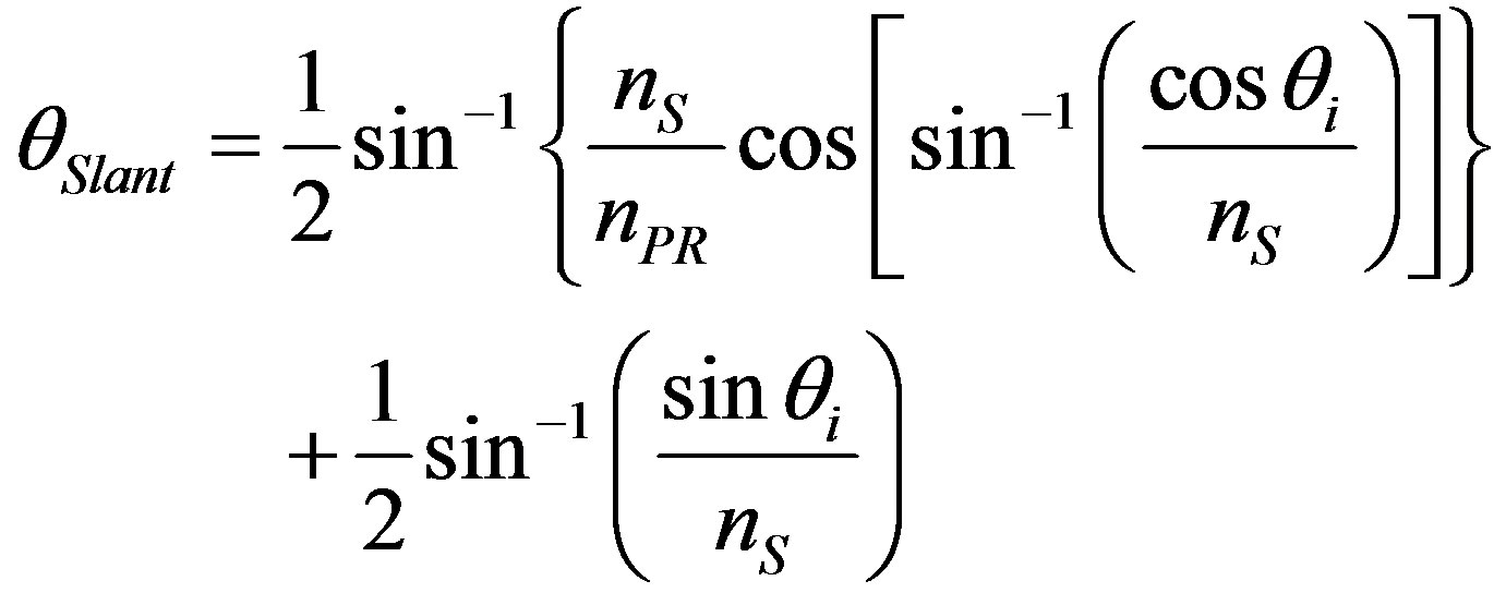 , (1)
, (1)
where nPR is the refractive index of photoresist at the laser wavelength. The slant period of the grating that can be measured directly on the top surface is evaluated by:
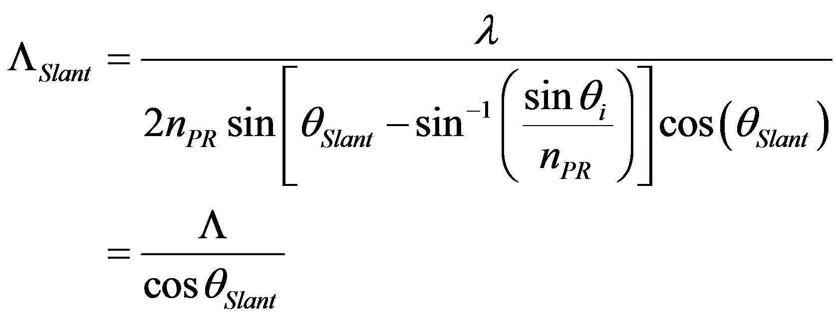 (2)
(2)
where Λ is correspondingly the “true” grating period if it is measured in the plane perpendicular to the side wall of the grating, as illustrated schematically in Figure 3. According to Figure 1, the effective area of the slant grating may be evaluated by the value of L with:
 , (3)
, (3)
where H is the thickness of the glass substrate.
In the practical fabrication, a single 355 nm laser beam is used as the UV light source, which is incident at an angle of θi = 34˚ onto the sample that is prepared by spin-coating S1805 photoresist from onto a fused-silica glass plate with a thickness of about 1.5 mm and an area of 10 ´ 10 mm2 at a speed of 2000 rpm. Furthermore, the glass substrate and the photoresist have a refractive index of nS = 1.476 and nPR = 1.74 at 355 nm, respectively. Thus, we can easily obtain ΛSlant = 31.66˚, ΛSlant = 536 nm, Λ = 456 nm, and L = 1.6 mm.
The atomic force microscopic (AFM) image of the fabricated slant grating is shown in Figure 2(a) and a three-dimensional (3D) re-drawing of Figure 2(a) is given in Figure 2(b). Clearly, the grating structures have a period of about 532 nm, or ΛSlant » 532 nm and Λ = 453 nm, which agrees very well the designed or the calculated values of ΛSlant = 536 nm and Λ = 456 nm. Figure 2(a) also shows a modulation depth smaller than 600 nm of the grating and Figure 2(b) indicates convincingly the slant features of the grating. The fabrication experiments
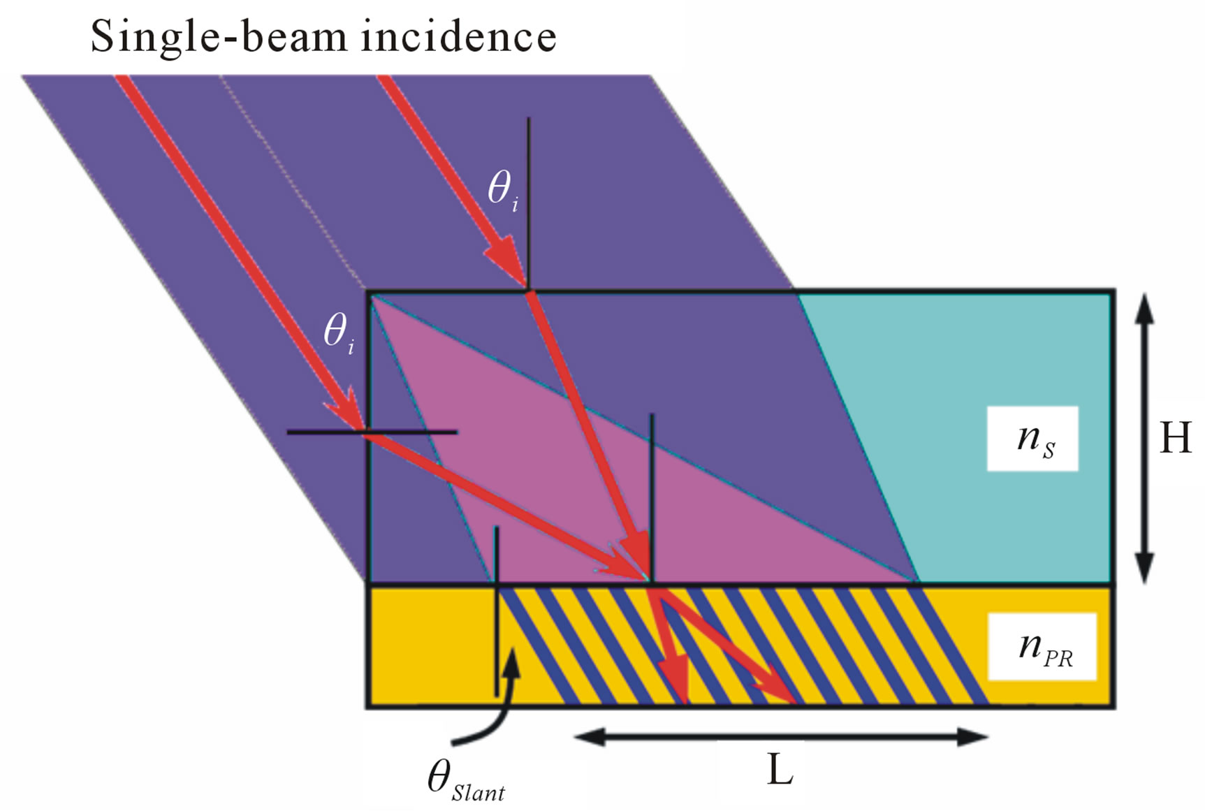
Figure 1. Schematic illustration of the single-beam interference lithography.
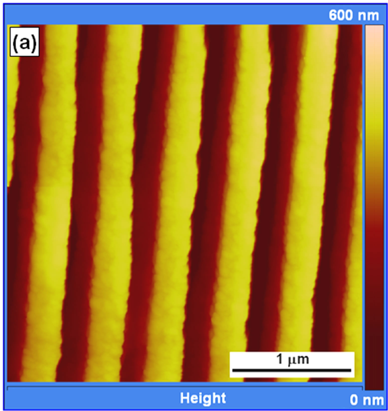
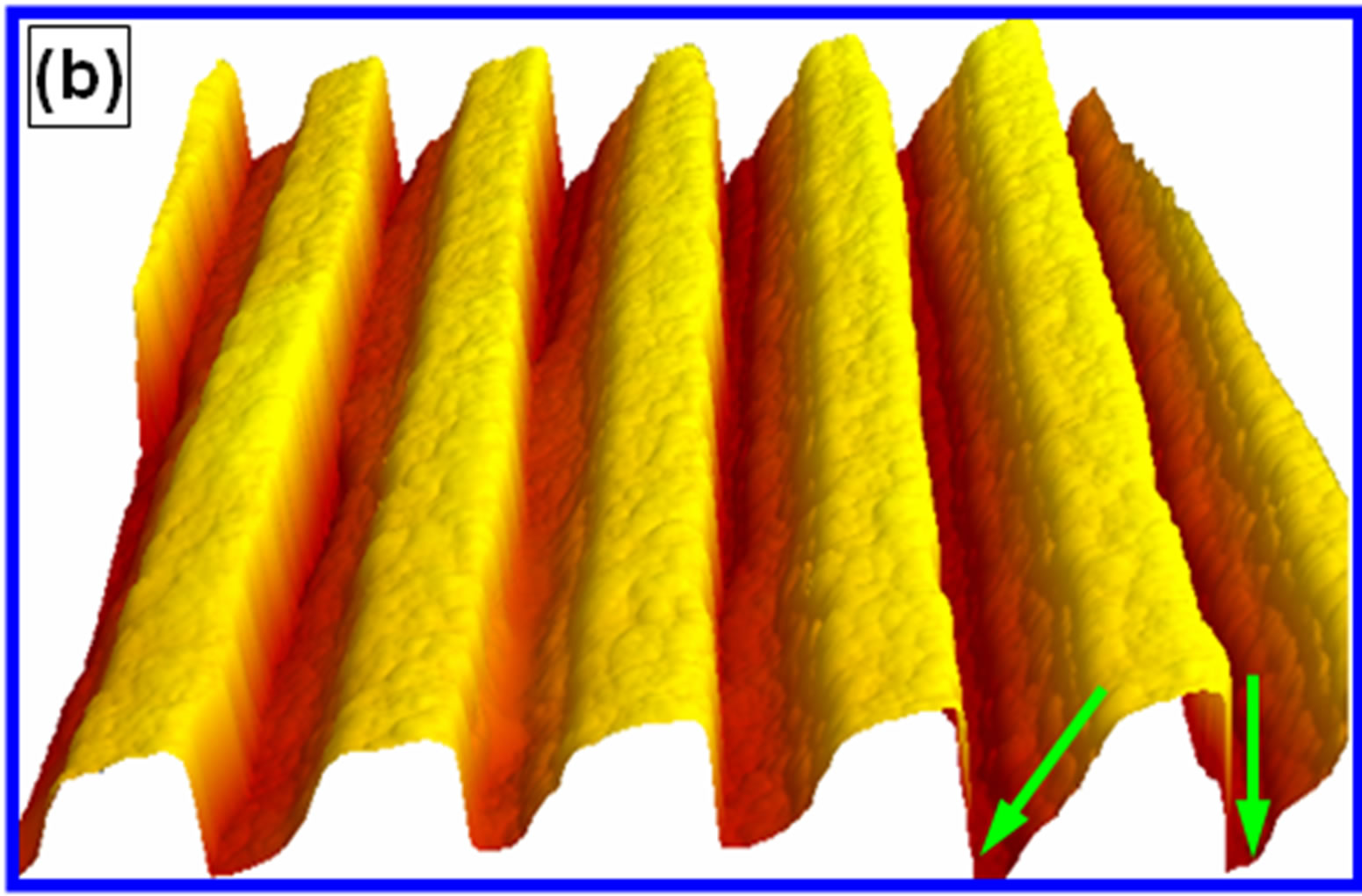
Figure 2. (a) AFM image of the photoresist slant grating structures; (b) A three-dimensional re-drawing of the AFM image in (a).
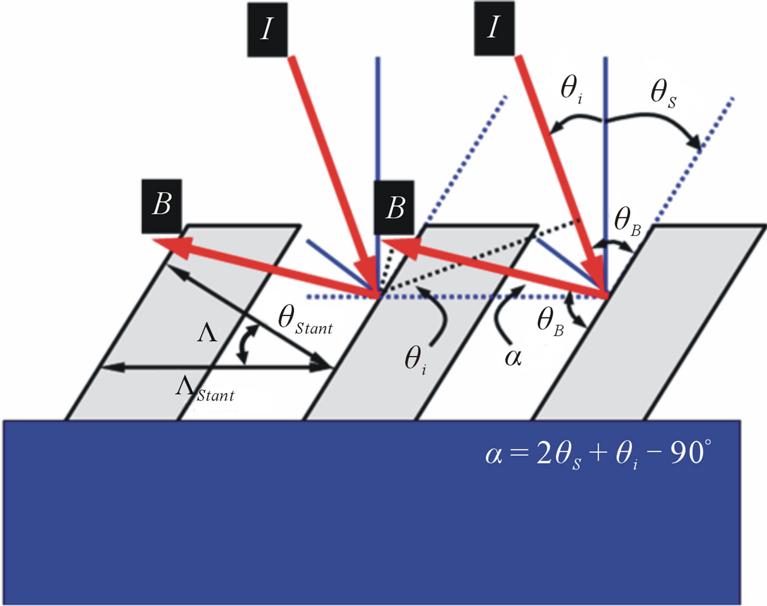
Figure 3. The schematic illustration of the Bragg-angle diffractions in the slant gratings.
showed that the period and the slant angle of the grating can be tuned by changing the incident angle of the UV laser. It should be noted that the laser beam coupled into the substrate through the side-wall will totally reflected by the top and bottom surfaces of the sample and propagates within the substrate, so that it interacts with the directly transmitted light multiple times within the photoresist layer. Thus, multiple domains of the interference patterns can be recorded as slant gratings in the photoresist, as can be observed in the inset of Figure 2(a), which actually extend the applicable grating area.
3. Bragg-Angle Diffractions in Slant Gratings
This kind of slant grating enables easily the Bragg-like diffractions even at normal incidence of light. The basic principles are illustrated schematically in Figure 3. The incident light at an angle of θi is actually incident at θB = θi + θSlant with respect to the side surface of the slant grating lines. If we look at the diffraction in the direction of beam B that is symmetric with the incident light beam I about the normal to the slant surface, which can be defined as a kind of Bragg-angle diffraction, the diffraction condition may be written as:  , where neff is the effective refractive index of the grating layer consisting of the air and photoresist, θB is the resonance wavelength of the Bragg-angle diffraction. Obviously, the value of neff is dependent not only on the duty cycle of the slant grating and the wavelength of the incident light, but also on the shape of the grating profile and how the light is incident onto the grating. Considering
 – 90˚, we have
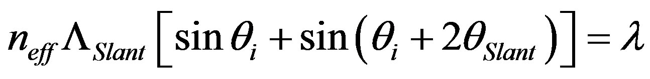 , which can actually be rewritten as:
 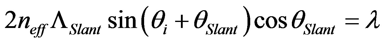 . However, we already obtained
 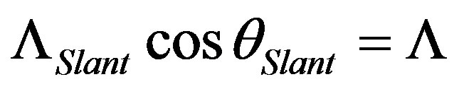 and θB = θi + θSlant, thus, the diffraction condition becomes:
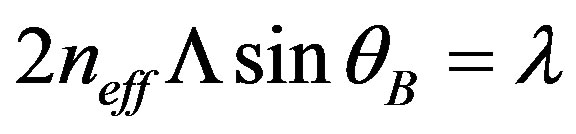 . (4)
. (4)
This is exactly the condition for Bragg diffraction and defines the Bragg-angle diffraction in the slant grating. On this basis, the slant gratings may be taken as a kind of one-dimensional photonic crystal structures that enables direct incidence from the side surface of the grating. It is this kind of Bragg-angle diffraction that induces strong spectroscopic response of the slant gratings.
Figure 4 presents the optical characterization of the device shown in Figure 2, which is demonstrated by the angle-resolved tuning properties of the optical extinction spectrum. The incident angle θi is changed from −44 to +36 degrees. The definitions of the positive and negative values of θi are illustrated in the inset of Figure 4(a). For a positive value of θi, a strong extinction signal with a bandwidth of about 90 nm at full width at half maximum (FWHM) can be observed, which is tuned from about 550 to 810 nm as the angle of incidence is increased from 0 to 28 degrees in steps of 4 degrees, as shown in Figure 4(a). For θi = 0, the spectral peak of the Bragg diffraction or the Bragg resonance mode is observed at about 550 nm. Using the Bragg diffraction condition in (4), a grating period of ΛSlant = 532 nm or Λ » 453 nm, a slant an-
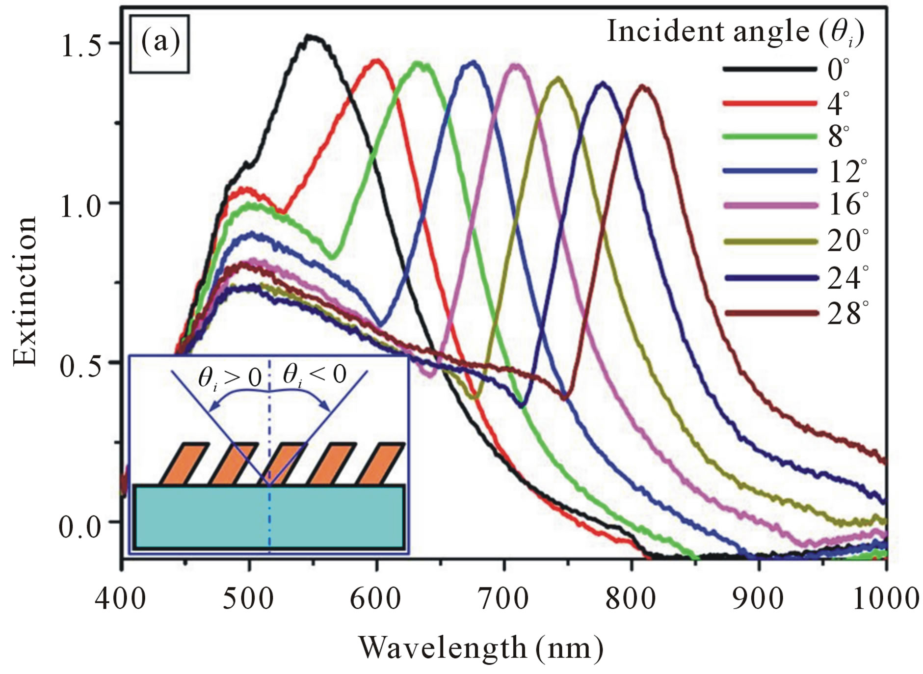
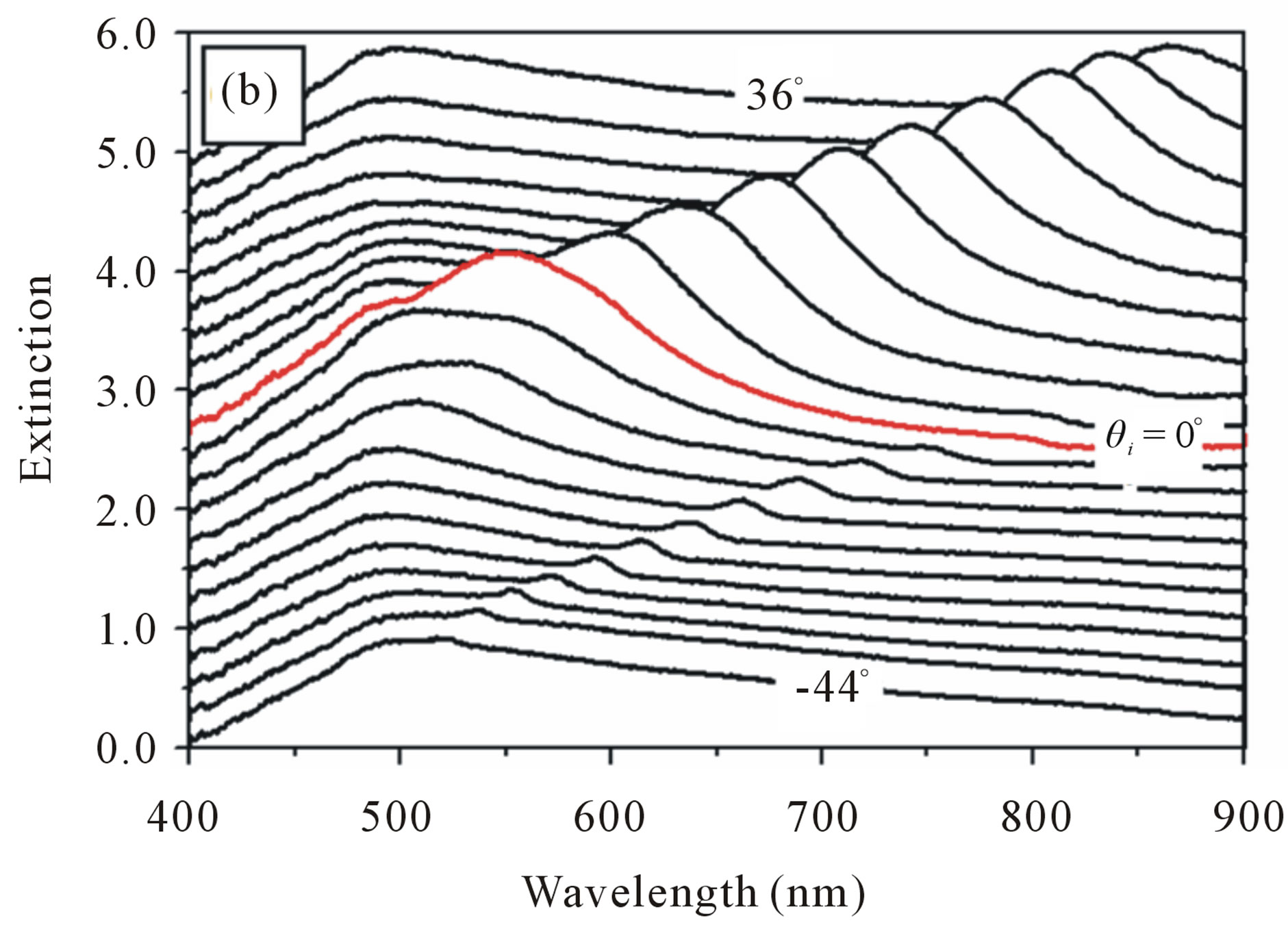
Figure 4. (a) Angle-resolved tuning properties of the Bragg resonance mode of the slant gratings for a positive incident angle increased from 0 to 28 degrees; (b) Angle-resolved tuning properties of the optical extinction spectrum with the incident angle changed from −44 to +36 degrees.
gle of ΛSlant » 31.66˚, we can obtain neff » 1.16 at about 550 nm for normal incidence.
As shown in Figure 4, the amplitude of the extinction signal due to the Bragg-angle diffraction is ranging from 1.4 to 1.6 (at θi = 0), meaning a reduction of 75% - 80% in the transmission spectrum. Furthermore, the resonance spectrum is tuned to longer wavelengths as the angle of incidence onto the slant surface of the grating is reduced while the incidence angle with respect to the normal of the substrate is increased. This is the typical feature of band-gaps of the one-dimensional photonic crystals.
For negative values of θi, a relatively small resonant mode with a bandwidth narrower than 10 nm at FWHM can be observed, which is tuned from about 790 to 520 nm as the incident angle is changed from 0 to −44˚. This is the shorter-wavelength branch of the waveguide resonance mode of the WGS structures [12], where a thin layer of photoresist remained at the bottom of the grating structures after the development process and it acts as the waveguide. Furthermore, a broad-band feature can be observed in addition to the above two tunable resonance modes, which is peaked at about 495 nm and extends to longer wavelengths with increasing the incident angle. This actually results from the normal grating diffraction and the absorption by the photoresist.
4. Conclusion
In conclusion, we demonstrated fabrication of slant gratings using a simple single-beam interference lithography scheme. The period and the slant angle of the grating structures may be tuned by changing the incident angle of the UV laser beam. Bragg-angle diffraction interprets the strong optical response of this kind of nanostructures with well-established theoretical model. The tunable resonance mode with a bandwidth of about 90 nm at FWHM may be taken as the band-gap of a kind of one dimensional photonic crystal structures. This introduces a new approach for the realization of photonic devices, which may be applied in filters and beam splitters, or used as master gratings for the realization of plasmonic devices.
5. Acknowledgements
The authors acknowledge the financial support by the National Science Foundation of China (11074018), the Program for New Century Excellent Talents in Uni- versity (NCET), and the Research Fund for the Doctoral Program of Higher Education of China (RFDP, 20091103110012).
REFERENCES
- W. W. Ng, C. S. Hong and A. Yariv, “Holographic Interference Lithography for Integrated-Optics,” IEEE Transactions on Electron Devices, Vol. 25, No. 10, 1978, pp. 1193-1200. doi:10.1109/T-ED.1978.19251
- V. Berger, O. Gauthier-Lafaye and E. Costard, “Photonic Band Gaps and Holography,” Journal of Applied Physics, Vol. 82, No. 1, 1997, pp. 60-64. doi:10.1063/1.365849
- A. Christ, S. G. Tikhodeev, N. A. Gippius, J. Kuhl and H. Giessen, “Waveguide-Plasmon Polaritons: Strong Coupling of Photonic and Electronic Resonances in A Metallic Photonic Crystal Slab,” Physical Review Letters, Vol. 91, No. 18, 2003, p. 183901. doi:10.1103/PhysRevLett.91.183901
- J. Stehr, J. Crewett, F. Schindler, R. Sperling, G. von Plessen, U. Lemmer, J. M. Lupton, T. A. Klar, J. Feldmann, A. W. Holleitner, M. Forster and U. Scherf, “A Low Threshold Polymer Laser Based on Metallic Nanoparticle Gratings,” Advanced Materials, Vol. 15, No. 20, 2003, pp. 1726-1729. doi:10.1002/adma.200305221
- X. P. Zhang, H. M. Liu, J. R. Tian, Y. R. Song and L. Wang, “Band-Selective Optical Polarizer Based on GoldNanowire Plasmonic Diffraction Gratings,” Nano Letters, Vol. 8, No. 9, 2008, pp. 2653-2658. doi:10.1021/nl0808435
- X. P. Zhang, H. M. Liu, J. R. Tian, Y. R. Song, L. Wang, J. Y. Song, and G. Z. Zhang, “Optical Polarizers Based on Gold Nanowires Fabricated Using Colloidal Gold Nanoparticles,” Nanotechnology, Vol. 19, No. 28, 2008, p. 285202. doi:10.1088/0957-4484/19/28/285202
- X. P. Zhang, B. Q. Sun, J. M. Hodgkiss and R. H. Friend, “Tunable Ultrafast Optical Switching via Waveguided Gold Nanowires” Advanced Materials, Vol. 20, No. 23, 2008, pp. 4455-4459. doi:10.1002/adma.200801162
- D. Nau, R. P. Bertram, K. Buse, T. Zentgraf, J. Kuhl, S. G. Tikhodeev, N. Gippius and H. Giessen, “Optical Switching in Metallic Photonic Crystal Slabs with Photoaddressable Polymers,” Applied Physics B—Lasers and Optics, Vol. 82, No. 4, 2006, pp. 543-547. doi:10.1007/s00340-005-2103-z
- X. L. Yang, L. Z. Cai and Y. R. Wang, “Larger Bandgaps of Two-Dimensional Triangular Photonic Crystals Fabricated by Holographic Lithography Can Be Realized by Recording Geometry Design,” Optics Express, Vol. 12, No. 24, 2004, pp. 5850-5856. doi:10.1364/OPEX.12.005850
- Y. Yang, Q. Li and G. P. Wang, “Design and Fabrication of Diverse Metamaterial Structures by Holographic Lithography,” Optics Express, Vol. 16, No. 15, 2008, pp. 11275-11280. doi:10.1364/OE.16.011275
- D. C. Meisel, M. Diem, M. Deubel, F. Pérez-Willard, S. Linden, D. Gerthsen, K. Busch and M. Wegener, “Shrinkage Precompensation of Holographic Three-Dimensional Photonic-Crystal Templates,” Advanced Materials, Vol. 18, No. 22, 2006, pp. 2964-2968. doi:10.1002/adma.200600412
- D. Rosenblatt, A. Sharon and A. A. Friesem, “Resonant Grating Waveguide Structures,” IEEE Journal of Quantum Electronics, Vol. 33, No. 11, 1997, pp. 2038-2059. doi:10.1109/3.641320
NOTES
*Corresponding author.