Journal of Surface Engineered Materials and Advanced Technology
Vol.4 No.5(2014), Article
ID:48724,8
pages
DOI:10.4236/jsemat.2014.45030
Transfer of Machined Patterns on an Aluminum Plate to Pyrex Glass Using Reactive Ion Etching SF6 Plasma without Masks
Carlos M. Ortiz-Lima, Fernando J. Quiñones-Novelo, Alberto Jaramillo-Núñez, Jorge Castro-Ramos
Insitituto Nacional de Astrofísica, Óptica y Electrónica, Puebla, México
Email: carlosortiz@inaoep.mx
Copyright © 2014 by authors and Scientific Research Publishing Inc.
This work is licensed under the Creative Commons Attribution International License (CC BY).
http://creativecommons.org/licenses/by/4.0/


Received 19 June 2014; revised 20 July 2014; accepted 7 August 2014
ABSTRACT
A method for etching the surface of a Pyrex glass substrate using the Reactive Ion Etching process without the use of masks is reported. Variations in the machined surface on an auxiliary plate, manufactured in aluminum and placed below a Pyrex glass slide, were transferred to the upper surface of the substrate. SF6 as etching gas and low pressure chamber to promote the increase of mean free path of ions were used. Two etching ratios were found, general, that affects the entire surface of the substrate, and differential, which generates the relief on the surface of the glass. Differential etching depth showed a linear behavior with respect to time; the mean differential etching rate obtained was 43 nm/min. The same phase between the auxiliary plate machining and the etched pattern on the substrate is preserved. With this technique it was possible to manufacture convex and concave surfaces; some examples are given. The arithmetic mean roughness achieved with the proposed method was found to be N1 class, ideal for the development of optical corrector plates.
Keywords:Reactive Ion Etching, No Masking RIE, SF6, Plasma Etching

1. Introduction
Reactive ion etching (RIE) is extensively used as an etching process. For RIE, a radio frequency power signal is applied from a stage, which is in contact with the substrate. In a plasma system, the electrons are accumulated on the stage. This accumulated charge, together with the electric field produced at the electrode by the current from the RF power, will produce an electric force [1] . In general the controlling mechanisms of the glass RIE process are the chemical reactions and physical effects such as the ion bombardment that enhances removal of the highly volatile reaction products [2] . A characteristic of RIE processes is that it leads to an anisotropic profile due to the directional nature of the ion bombardment, affecting the surface of a substrate in the form of chemical reactions as well as physical sputtering [3] . Fluorine based plasma etching using RIE is a widely used technique for etching deep structures in silicon, silica and glass and it is considered as a good choice for mass manufacturing [4] .
One of the limiting factors in incorporating glass into microdevices is its limited machinability [5] , however some benefits in glass machining can be found. Glass has many advantages such as good mechanical properties, good optical properties, and high electrical insulation [6] . Applications in microoptics and substrate of micrototal system [2] have been developed. Particularly, in optical applications, silica and glass are considered superior to silicon in microfabrication, when optical transparency, low electrical conductance and biocompatibility are required [4] .
The most widely used etching method by using RIE process is transferring a master pattern through a lithographic process on the substrate in order to etch the complementary pattern. Sections on the substrate which are covered with lithographic material generally remain intact after the etching process. Many techniques for masking have been developed besides photo resist, such as shadow mask in Si and glass using a reusable nonbonded silicon shadow mask, which consist in a through-hole on a Si wafer [4] ; in contrast, another method consists in the fabrication of a silicon wafer bonded to a borosilicate glass wafer by anodic bonding to be used as an etching mask [7] .
The principal requirements for a good mask material are that it can be easily patterned, it has a high selectivity compared to the material to be etched (for good pattern transfer and high resolution) and it must be possible to selectively remove the mask material from the substrate after etching [8] ; in any event, plasma etching requires optimization of the etching parameters and suitable choice of masking material for each application [4] .
A variety of materials and techniques have been used to mask glass substrates. Such materials are, for example, Ni masks generated by selective electro deposition on a previously made grooves-pattern of photo resist on a glass substrate in order to generate surface reliefs using plasma [2] [3] [9] . Another masking technique consists in recording a film of Cr and standard photo resist for etching a Pyrex glass substrate [10] .
Any new technology requires new machining skills [5] . In this work, a pattern machined on a block of aluminum is transferred to a Pyrex glass surface without using masking materials.
2. Experimental Setup
On a block of aluminum, a master pattern is defined by a machining process. This piece is called modulator plate (MP). The MP is placed on the stage inside the vacuum chamber. The stage is chilled by water circulating inside at 4˚C. A slide of 200µm thick Pyrex glass is placed on the top of the MP. Figure 1 is an outline of the overall experimental scheme. An iron-ferrite permanent magnet is installed on the stage (not showed) to densify the plasma. The MP is made of 6061 type aluminum. On its surface there is a series of machined grooves triangle-shaped cross section forming concentric circles made by using a semiautomatic lathe. The length of the machined period is 500 µm and 430 µm depth to form an equilateral triangle shape cross section.
The expected result is that the upper surface of the substrate becomes etched in the way of the master pattern machined on the MP. Figure 2 shows a scheme of the expected results after transferring the master pattern on the MP directly to the substrate.
Figure 3 is a set of two photographs showing in detail the machined master pattern on the MP.
3. The Synergetic Mechanism of the Modulator Plate
During the RIE process, a self-bias DC voltage is established between the RF-powered stage and the grounded chamber due to the accumulation of electrons on the stage after dissociation of the etchant gas molecules during the plasma process [11] . Equipotential surfaces are generated over all the internal volume of the chamber, and they follow the contour of every surface on its vicinity.
To explain the etching process on the glass substrate in the method proposed in this paper, it can be thought
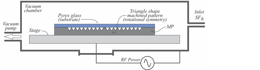
Figure 1. Scheme of the experimental setup. The MP is placed on the stage in the RIE system; on the top surface of the MP a 200µm thick slide of Pyrex glass is installed.

Figure 2. Scheme of the master pattern transferred to the substrate.
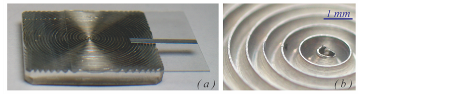
Figure 3. Photographs of the MP. (a) shows the entire MP and a glass slide placed on it; (b) is a zoom detail of the master pattern machined on the MP.
that on a stage with a flat and horizontally positioned upper surface, the generated equipotential surfaces lie parallel to it. Figure 4(a) shows the case when the surface contour is flat. If the original flat surface of the stage is adapted to a different relief, the distribution of the equipotential surfaces will be modified depending on the new distribution of the electric field which, in turn, depends on the shape of the new stage surface. Figure 4(b) shows the case of a triangle shape surface. This new surface on the stage corresponds to the concept of MP.
In a typical RIE-masking setup such as that showed in Figure 4(a), the etched zones generally result on a relatively flat and horizontal bottom surface and almost vertical side walls, whereas, a new distribution of electric field, and thus the equipotential surfaces, allows the removal of material preferably on specific regions of the substrate surface, following approximately the shape of the equipotential surface located on the top of the substrate. Figure 4(c) displays in red the contour followed by an etching process over a hypothetic nth equipotential surface on a substrate. In the vicinity of the MP, the distribution of the electric field will work as spatial modulator that redistributes the ion bombardment on the substrate surface.
Figure 4(c) also depicts the result of the etching process. A substrate placed on the top of the MP, enclosed in a dashed line rectangle, is divided into two parts. The upper green part represents the material removed by the ion bombardment and its height depends on the duration of the process. The bottom blue part represents the remaining substrate after the etching process on which the pattern machined on the MP has been transferred to its surface. Each one of the n equipotential surfaces outlined on Figure 4(b) can be achieved only by extending the process time.
The importance of MP is that performs the electric field distribution in the vicinity of the MP and produces redistribution in the precipitation of ions on the substrate surface, following the grooves pattern machined on the MP.

Figure 4. Scheme of the nth equipotential surface transferred to the substrate by nonmasking RIE.
4. Experimental Results
Glasses containing oxides other than silica or boron oxide, such as Pyrex, produce nonvolatile fluorides that redeposit in the etching equipment, if they leave the etched area at all [4] . Pyrex glass also contains Na and Al which generate nonvolatile products such as NaF y AlF3 when using SF6 as etchant gas, so it is necessary to promote physical sputter-etching of these products by setting up specific process parameters in order to increase the free path of ions and the bombardment effect [2] . Such parameters are low chamber pressure and high self-bias voltage.
The experiments in this work were carried out by varying the etching time. In order to determine the selectivity of the surface etching, two types of surface etching are proposed, a general etching or etching depth and a differential etching. General etching is produced because the entire surface of the substrate is subjected to ion bombardment; this kind of etching is inherent to the process due to no masks are placed on the substrate to protect it. Differential etching occurs due to the redistribution of the electric field on the surface of the MP. Figure 5 outlines the concept of general and differential etching in comparison of a control surface.
The parameters used in the RIE processes without masks are summarized in Table1
Figure 6 shows three images of the surface pattern obtained under the conditions described in Table1 The specimen surface showed in Figure 6(a) was obtained with a WYKO NT1100 interferometric optical profiling system. Figure 6(b) and Figure 6(c) are photographs of interferograms obtained by an amplitude division interferometer which shows the optical path difference between the upper and lower surfaces of the substrate; the lower surface is flat and serves as a reference surface. In particular, Figure 6(c) verifies phase alignment of circular profile machined on the MP and the phase of the etched surface on the substrate if it is compared with the photograph presented in Figure 3(b). This means that there is a match between a peak and a valley in the pattern machined on the MP and a peak and a valley etched on the surface of the substrate.
The results presented in Figure 6 show that, by using the method proposed, it is possible to manufacture concave and convex shape surfaces according to the MP machined pattern.
Figure 7 is an example of the profiles that were used to determine the etching depth in different processes. Figure 7(a) shows the extent of differential etching depth obtained in a three-minute etching process; Figure 7(b) displays the length of the period in the etched surface on the substrate, which coincides with the period of the machined pattern on the MP. Measurements of profiles were obtained with the same equipment as that used to generate the surface of Figure 6(a).
The arithmetic mean roughness recorded on the glass substrate is N1 class, which potentiates the proposed method for manufacturing optical elements.
According with the parameters of the RIE process given in Table 1, the mean general etching rate resulted in 305nm/min. That is always greater than the mean differential etching rate, which is 43 nm/min. Figure 8 shows the differential etching depth obtained in the experiments as a function of time.
Data presented in Figure 8 show that in a RIE process of approximately 6.5 minutes long, the differential etching depth reaches the value of λ/2 with reference to the central wavelength of the visible spectrum. This is a parameter that can serve as reference if the proposed method is used in the manufacturing of corrector plates to reduce spherical aberration in optical systems. An example of such plates is the Schmidt Corrector Plate, which can require an etching depth of about 0.15λ following a fourth degree surface. The possibility that the surface shape generated during the etching process on the substrate follows a relief previously machined on the MP enables the possibility of manufacturing Free Form Corrector Plates, which could be not dependent on a rotational symmetry.

Figure 5. Scheme of general and differential etching.

Table 1. Parameters set in RIE etching process.
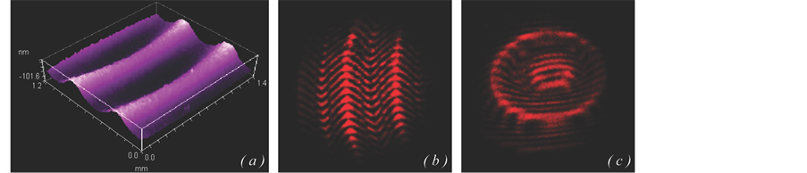
Figure 6. Interferometric images that show the surface relief of a Pyrex glass substrate using the RIE without masks method under the conditions given in Table1

Figure 7. Measurement of the differential etching obtained in one sample in a three-minute etching process.
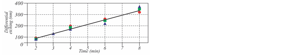
Figure 8. Differential etching depth obtained as a result of the experiments.
5. Comments
It was found that during the RIE etching process in the experiments, the magnitude of the self-bias voltage decreased with time due to temperature increase on the plate and magnet. The diagram in Figure 9 shows the self-bias voltage versus time.
Etching depth showed a linear behavior (as depicted in Figure 8), which is expected if only fixed time periods are added to each consecutive etching process. In particular, differential etching rate is not constant in the processes subjected to different etching time. Figure 10 shows the behavior of the differential etching rate as a function of time.
The reduction in the differential etching ratio is attributed to the increment of temperature on the stage and the magnet, in the same way as the decrement of self-bias voltage.
The film of AlF3 and NaF formed on the substrate surface increases if the etching process lasts more than four minutes. The solution to this problem was to set the maximum etching time to four minutes; if a process was planned to last more than four minutes, that was divided into two periods of time in order to give an opportunity to the components in the vacuum chamber to reduce their temperature, then the procedure was reinitiated until the specified process time was achieved.
Differential etching depth was strongly affected in processes lasted over four minutes. Figure 11 shows an example of a generated surface whose etching time was eight consecutive minutes. In Figure 11(a) it is possible to observe an interferometric image of a sample in which the roughness on the substrate surface is much higher respect of an etching process developed in shorter periods of time, proving to be an order of magnitude higher. This can be verified by comparing Figure 11(b) and Figure 7.
It should be noted that the results presented were obtained without the use of cryogenic procedures to reduce the temperature of the elements in the vacuum chamber. Diagram in Figure 10 shows a drift on the differential etching rate of 5% throughout the experiments only by taking short periods of RIE process time to decrease temperature inside the chamber.
It was also built a MP which surface was covered by stainless steel needles of 600 µm diameter in order to generate cylindrical-type surfaces. The resultant etching shape is showed in Figure 12. The etching was carried out under the conditions outlined in Table1
In the etching method proposed in this work, the MP, which contains spatial information that is transferred to the substrate, is always placed under the glass slide; the glass slide works as a protecting cover from the ion bombardment so minimum damage on the metal surface is carried out on the plate by the RIE process. This way of etching a substrate surface is suitable for mass production by reutilization of MP.
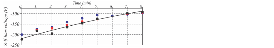
Figure 9. Self-bias voltage generated in vacuum chamber versus time.
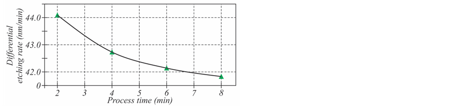
Figure 10. Decrease of differential etching versus time.
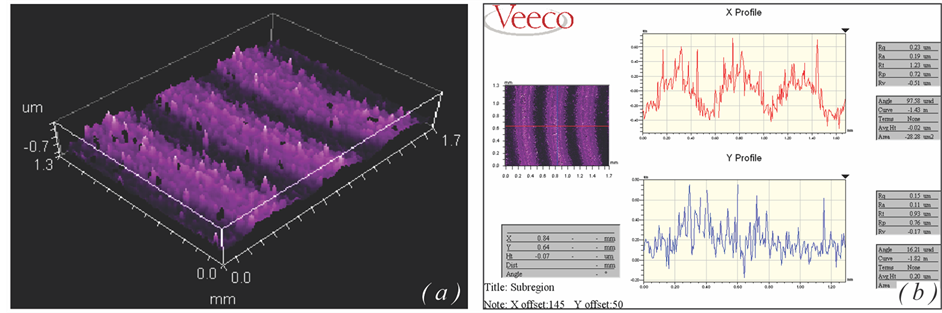
Figure 11. Roughness increases and the differential etching depth decreases as the etching process was maintained for more than four successive minutes. The image shows a surface that was subjected to eight consecutive minutes etching process.
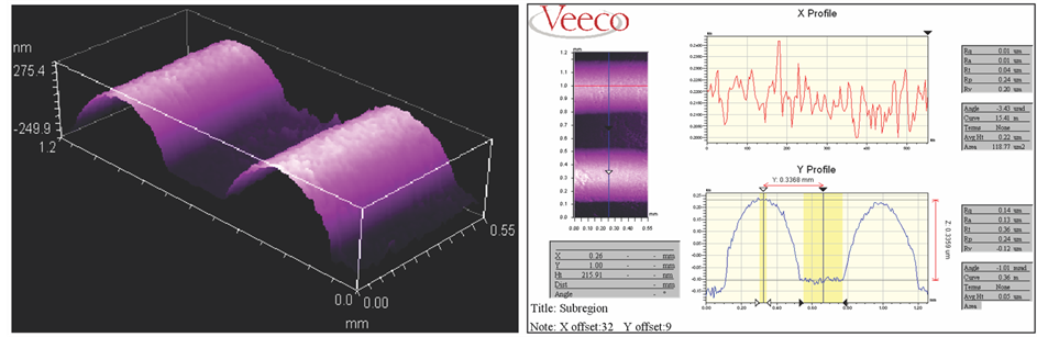
Figure 12. A cylindrical-type surface is generated by the proposed etching method.
The manufacturing of the MP is presented as a challenge to reduce the period of the etched profile on the substrate. Minimum groove width on the MP depends on the capabilities of the machining process and the materials involved. The relatively low yield point of aluminum 6061 limits the manufacturing of small size grooves. The normal strength due to the approximation of the triangular shaped tool bit to the work piece generates perpendicular stress which pushes and displaces the superficial material, causing plastic deformation on the grooves previously manufactured. After the machining process, some chip remains attached to the metal, particularly on the edges of the pattern; surface finishing has to be accomplished in order to couple the MP and the flat substrate prior to the plasma process. Experimentally it was determined that an equilateral triangle 500 µm period represents a profitable groove shape, which provides a wide enough aluminum cross section to avoid plastic deformations and enables enough space to perform the surface finishing.
6. Conclusion
Transfer surface patterns using the RIE technique generally require a masking process. In this work, a technique that allows a pattern machined on a piece of aluminum to be transferred to the upper surface of a Pyrex glass substrate without the use of any masking process was presented. Technical details used in the preparation of the experiments in the different processed plates were discussed. Concaves and convex surfaces N1 class roughness were accomplished; these kinds of surfaces are ideal for applications in the field of optics, especially in applications such as corrector plates, which etched depth requires commonly distances lower than one optical wavelength. Massive production of etched substrates is suitable due to the possibility of MP reuse.
Acknowledgements
C.M.O.L. tanks to Francisco Renero-Carrillo for his valuable contribution in obtaining the interferometric images, to Claudia Reyes-Betanzo for accommodating our activities in the Microelectronics Laboratory at the Instituto Nacional de Astrofísica Óptica y Electrónica, and to Marco De-Jesus-Ortiz for his contribution in the development of metal machining.
References
- Choe, H.H. (2006) Basic Study of a Glass Substrate in Dry Etching System. Vacuum, 81, 344-346.http://dx.doi.org/10.1016/j.vacuum.2006.06.010
- Li, X., Abe, T. and Esashi, M. (2001) Deep Reactive Ion etching of Pyrex Glass Using SF6 Plasma. Sensors and Actuators, A87, 139-145. http://dx.doi.org/10.1016/s0924-4247(00)00482-9
- Park, J.H., Lee, N.-E., Lee J., Park, J.S. and Park, H.D. (2005) Deep Dry Etching of Borosilicate Glass by Using SF6 and SF6/Ar Inductively Coupled Plasmas. Microelectronic Engineering, 82, 119-128.http://dx.doi.org/10.1016/j.mee.2005.07.006
- Kolari, K. (2007) Deep Plasma Etching of Glass with a Silicon Shadow Mask. Sensors and Actuators, A141, 677-684.http://dx.doi.org/10.1016/j.sna.2007.09.005
- Wüthrich, R. (2009) Micromachining Using Electrochemical Discharge Phenomenon: Fundamentals and Applications of Spark Assisted Chemical Engraving. 1st Edition, William Andrew Applied Science Publishers, USA.http://dx.doi.org/10.1016/b978-0-8155-1587-6.50006-2
- Bu, M., Melvin, T., Ensell, G.J., Wilkinson, J.S. and Evans, A.G.R. (2004) A New Masking Technology for Deep Glass Etching and Its Microfluidic Application. Sensors and Actuators, A115, 476-482.http://dx.doi.org/10.1016/j.sna.2003.12.013
- Akashi, T. and Yoshimura, Y. (2006) Deep Reactive Ion Etching of Borosilicate Glass Using an Anodically Bonded Silicon Wafer as an Etching Mask. Journal of Micromechanics and Microengineering, 16, 1051-1056.http://dx.doi.org/10.1088/0960-1317/16/5/024
- Bradley, J.D.B., Ay, F., Wörhoff, K. and Pollnau, M. (2007) Fabrication of Low-Loss Channel Waveguides in Al2O3 and Y2O3 Layers by Inductively Coupled Plasma Reactive Ion Etching. Applied Physics, B89, 300-318.http://dx.doi.org/10.1007/s00340-007-2815-3
- Park, J.H., N.-E., Lee, J. and Lee, J. (2005) Deep Reactive Ion Etching of Borosilicate Glass by sing SF6 and SF6/Ar Inductively Coupled Plasmas. Journal of Korean Physical Society, 47, S422-S428.http://dx.doi.org/10.1016/j.mee.2005.07.006
- Chabloz, M., Jiao, J., Yoshida, Y., Matsuura, T. and Tsutsumi, K. (2000) A Method to Evade Microloading Effect in Deep Reactive Ion Etching for Anodically Bonded Glass-Silicon Structures. MEMS 2000 0-7803-5273-4/00, 283-287.http://dx.doi.org/10.1109/memsys.2000.838530
- Hansen, H., Gardeniers, H., de-Boer, M., Elwenspoek, M. and Fluitman, J. (1996) A Survey on Reactive Ion Etching of Silicon in Microtechnology. Journal of Micromechanics and Microengineering, 6, 14-28.http://dx.doi.org/10.1088/0960-1317/6/1/002