New Journal of Glass and Ceramics
Vol.2 No.1(2012), Article ID:16977,4 pages DOI:10.4236/njgc.2012.21003
Growth and Electrical Properties of Doped ZnO by Electrochemical Deposition
![]()
School of Materials Science and Engineering, University of New South Wales, Sydney, Australia.
Email: *D.Chu@unsw.edu.au
Received August 30th, 2011; revised October 6th, 2011; accepted October 7th, 2011
Keywords: ZnO Electrochemcial Deposition
ABSTRACT
In this work, pure and different metal ions doped ZnO thin films were obtained by a facile electrochemical deposition process. Different morphologies of ZnO, such as nanoplates, nanoparticles, as well as dense film can be obtained by doping Cu2+, In3+, and Al3+, respectively. Besides, the electrical properties of ZnO were also dependent on the doping ions. In this work, only pure ZnO shows resistive switching characteristics, indicating that the defects in ZnO is a key role in inducing resistive switching behaviour.
1. Introduction
As a wide band gap II-VI semiconductor, zinc oxide (ZnO) has many applications such as transducers, gas sensors, and dye-sensitized solar cells, etc. [1-5]. Specially, ZnO thin films have attracted considerable attention because they can be tailored to possess high electrical conductivity and high visible transmittance by different coating techniques. For example, ZnO films have been deposited for resistive random access memory (RRAM) applications [6-8]. In these cases, ZnO films with well aligned sheets, rods, or wires may exhibit better performance, because of fast and effective path for electron transportation. Therefore, it is essential to control the morphology of ZnO films for potential RRAM applications.
To date, various physical and chemical methods have been developed to fabricate ZnO thin films. For instance, pulsed laser deposition, radiofrequency magnetron sputtering, metal-organic chemical vapor deposition (MOCVD), a vapor-liquid-solid mechanism, spray pyrolysis, sol-gel, and have been reported [9-11]. In most cases, high temperature and special atmosphere are necessary, which go against large-scale and low-cost production of ZnO films. In contrast, electrochemical deposition method represents a simple and effective route to control the morphology and composition of ZnO films [12,13]. Most reports on ZnO films prepared by electrochemical deposition method are focused on their morphology and optical properties, while only a few researches mentioned their electrical properties [14-16]. For RRAM applications, control of their electrical properties is very important to achieve high performance. Therefore, it is worthwhile to investigate the relationship between the structure, composition and electrical properties of ZnO films prepared by electrochemical method. In this paper, different metal ions doped ZnO films were deposited and the effects of doping ions on the electrical properties were investigated.
2. Experimental
Electrodeposition was carried out using a HA151 Potentiostat (Hokuto Denko Corporation, Japan). A standard three-electrode setup in an undivided cell was used. FTO (9.3 ~ 9.7 Ω, Asashi Glass Corporation, Japan, 1.1 mm × 26 mm × 30 mm) was used as the working electrode while platinum foil (0.2 mm × mm 10 mm × 20 mm) was used as the counter electrode. The distance between the two electrodes was 30 mm. The reference electrode was an Ag/AgCl electrode in 4 M KCl solution, against which all the potentials reported herein were measured.
The FTO ubstrates were first cleaned by ethanol and acetone sonication/ultra-violet ozone and electrodeposited in a solution of 0.01 M Zn(NO3)2∙6H2O and different amount of dopants at 2 mA for 30 min, at 75˚C. The phase composition of the samples was characterized by X-ray powder diffraction (XRD, RINT-2100V, Rigaku, Cu Kα). The morphologies of the samples were observed by field emission scanning electron microscopy (FESEM; JSM-6335FM, JEOL, with an accelerating voltage of 5 kV). A Keithley 6517B source meter was used for electrical characterization.
3. Results and Discussion
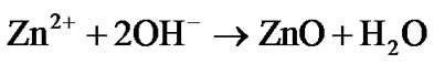
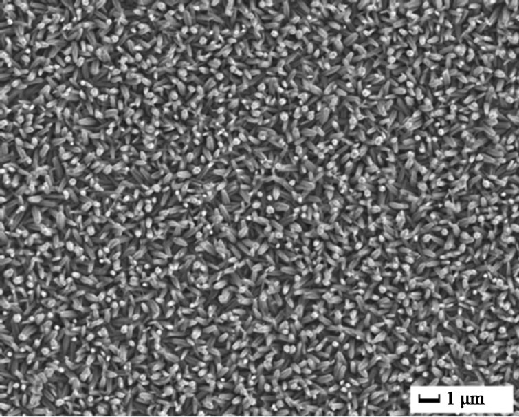
The surface morphology of undoped and doped ZnO films was illustrated by SEM, as shown in Figure 1. For undoped ZnO, oriented nanorod arrays with average diameter of 200 nm were obtained under 2 mA, 70˚C, 30 min. This is consistent with other reports about ZnO nanorods array from electrochemical deposition. As to 5 at% Cu2+ doped ZnO, it is interesting that nanoplates instead of nanorods were found. The average thickness of the nanoplates was 200 nm and their diameter could reach several micrometers. More interestingly, In3+ doping resulted in small nanoparticles with size less than 150 nm. Further, continuous film was obtained by 5 at% Al3+ doping. It is obvious that doping ions had great effects on the morphology of ZnO films. Usually, electrodeposition of ZnO is based on the generation of hydroxide ions
(OH–) at the surface of the electrode by the cathodic reduction of oxygen precursor in a Zn(NO3)2 solution. The Zn2+ and OH– ions react together, leading to ZnO deposition on the surface of the cathode according the following formulas:

Usually, ZnO grows preferentially along [0 0 1] direction in aqueous solution because of the lowest surface energy of (0 0 1) facet. And the growth velocity along [0 1 0] directions is slower than that of [0 0 1] direction, resulting in nanorod morphology. In the presence of doping ions, then can serve as structure-directing agent to adsorb selectively on ZnO basal planes and modify this surface chemistry properties. For example, Cu2+ ions might be adsorbed on the (0 0 1) facets of ZnO crystals and significantly decrease the growth rate of these facets,
 (a)
(a)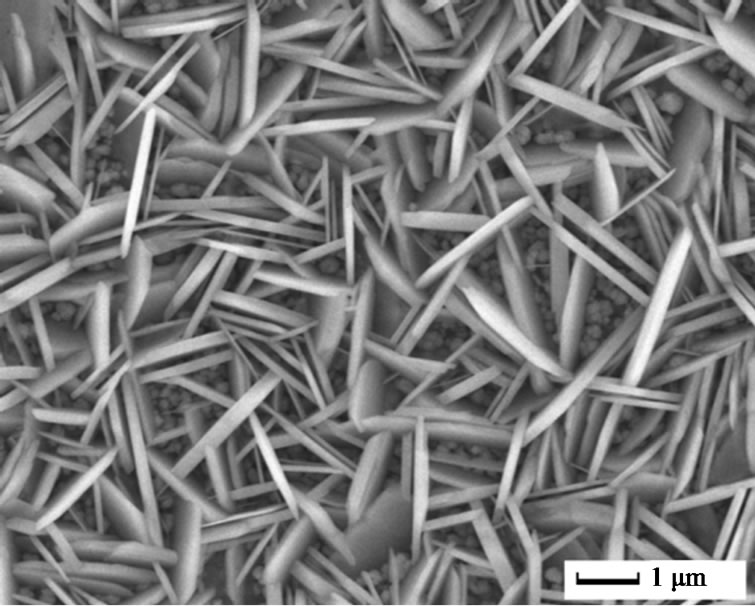 (b)
(b) (c)
(c) (d)
(d)
Figure 1. SEM images of pure and different ions doped ZnO: (a) Pure; (b) 5 at% Cu2+; (c) 5 at% In3+; and (d) 5 at% Al3+.
 (a)
(a)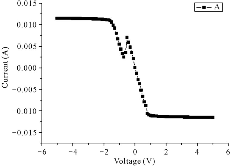 (b)
(b)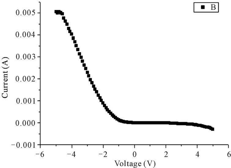 (c)
(c)
Figure 2. Typical I-V characteristics of (a) Pure ZnO; (b) In3+ doped ZnO; and (c) Al3+ doped ZnO based on the FTO/ZnO/Pt structure.
resulting in plate-like structure. As to In3+ ions doped ZnO, In3+ ions might be adsorbed on the different surfaces and small nanoparticles were then obtained.
The typical I-V characteristics of pure and doped ZnO were shown in Figure 2, where the voltage was swept from –5 V to 5 V. For pure ZnO, by sweeping the voltage from –5 V to a certain voltage of about –1.8 V, a sudden drop of leakage current is observed, indicating the resistance has switched to high resistance state, and non-volatile off state is achieved. While sweepingthe voltage to positive regions, an abrupt jump of leakage current appears at a higher voltage of 2.5 V is found. Interestingly, for In3+ and Al3+ doped ZnO, they do not show resistance switching behaviour, as indicated in Figures 2(b) and (c). Specially, In3+ doped ZnO shows a rectifying behaviour, indicating formation of a ZnO/Pt diode heterojunction. As to Al3+ doped ZnO, a linear I-V curve in the region of –2 V to 1 V can be observed and the current was saturated at higher voltage, which suggested that the conductivity has been increased by Al3+ doping.
The mechanism for resistive switching related properties of doped ZnO is interesting but still controversial. Among many proposed models, the filamentary mechanism may explain the resistance switching effect in this work. According to this model, the filaments are composed of defects such as oxygen vacancies. Therefore, these defects are essential to the electrical properties, which can be controlled by selective doping.
4. Conclusion
In summary, pure and doped ZnO thin films were prepared by electrochemical deposition at low temperature. ZnO nanoplates, nanoparticles, as well as dense film can be obtained by doping Cu2+, In3+, and Al3+, respectively. Besides, the electrical properties of ZnO were also dependent on the doping ions. In this work, only pure ZnO shows resistive switching characteristics, indicating that the defects in ZnO is a key role in inducing resistive switching behaviour.
REFERENCES
- Photonic, “ZnO Oxide Materials and Devices II,” Photonic Conference Abstract, 2007.
- W. Wang, H.-M. Huang, Z.-Y. Li, H.-N. Zhang, Y. Wang, W. Zheng and C. Wang, “Zinc Oxide Nanofiber Gas Sensors via Electrospinning,” Journal of the American Ceramic Society, Vol. 91, No. 1, 2008, pp. 3817-3819.
- E. Hosono, S. Fujihara and T. Kimura, “Synthesis, Structure and Photoelectrochemical Performance of Micro/ Nano-Textured ZnO/Eosin Y Electrodes,” Electrochimica Acta, Vol. 49, No. 14, 2004, pp. 2287-2293. doi:10.1016/j.electacta.2004.01.009
- X. L. Hu, et al., “Synthesis of Well-Aligned ZnO Nanowhisker Films Using Aqueous Solution for Use in DyeSensitized Sensor,” Key Engineering Materials, Vol. 388, 2009, pp. 27-30.
- Y. G. Wang, M. Sakurai and M. Aono, “Mass Production of ZnO Nanotetrapods by a Flowing Gas Phase Reaction Method,” Nanotechnology, Vol. 19, No. 24, 2008, p. 5. doi:10.1088/0957-4484/19/24/245610
- W.-Y. Chang, et al., “Resistive Switching Behaviors of ZnO Nanorod Layers,” Applied Physics Letters, Vol. 96, No. 24, 2010, Article ID: 242109-3. doi:10.1063/1.3453450
- J. W. Seo, et al., “A ZnO Cross-Bar Array Resistive Random Access Memory Stacked with Heterostructure Diodes for Eliminating the Sneak Current Effect,” Applied Physics Letters, Vol. 98, No. 23, 2011, Article ID: 233505-3. doi:10.1063/1.3599707
- L. Kukreja, A. Das and P. Misra, “Studies on Nonvolatile Resistance Memory Switching in ZnO Thin Films,” Bulletin of Materials Science, Vol. 32, No. 3, 2009, pp. 247- 252. doi:10.1007/s12034-009-0037-5
- J. Zou, et al., “Optical Properties of ZnO Thin Film on γ- LiAlO2 Substrate Grown by Pulsed Laser Deposition,” Thin Solid Films, Vol. 496, No. 2, 2006, pp. 205-207. doi:10.1016/j.tsf.2005.08.315
- M. Ohyama, et al., “Preparation of ZnO Films with Preferential Orientation by Sol-Gel Method,” Journal of the Ceramic Society of Japan, Vol. 104, No. 4, 1996, pp. 296- 300. doi:10.2109/jcersj.104.296
- S. Sun, et al., “Controlled Growth and Optical Properties of One-Dimensional ZnO Nanostructures on SnO2 Nanobelts,” Crystal Growth & Design, Vol. 7, No. 10, 2007, pp. 1988-1991. doi:10.1021/cg0701776
- F. J. Sheini, D. S. Joag and M. A. More, “Electrochemical Synthesis of Sn Doped ZnO Nanowires on Zinc Foil and Their Field Emission Studies,” Thin Solid Films, Vol. 519, No. 1, 2010, pp. 184-189. doi:10.1016/j.tsf.2010.07.106
- C.-T. Hsieh, J.-Y. Lin and S.-Y. Yang, “Low Temperature Growth of ZnO Nanorods on Flexible Polymeric Substrates,” Physica E: Low-Dimensional Systems and Nanostructures, Vol. 42, No. 9, 2010, pp. 2319-2323. doi:10.1016/j.physe.2010.05.008
- G. W. She, et al., “Controlled Synthesis of Oriented Single-Crystal ZnO Nanotube Arrays on Trenasparent Conductive Substrates,” Applied Physics Letters, Vol. 92, No. 5, 2008, p. 053111. doi:10.1063/1.2842386
- M. A. McLachlan, et al., “Electrochemical Deposition of Ordered Macroporous ZnO on Transparent Conducting Electrodes,” Materials Chemistry and Physics, Vol. 129, No. 1-2, 2011, pp. 343-348. doi:10.1016/j.matchemphys.2011.04.021
- O. Ozcan, et al., “Effect of Hydrogen and Oxygen Plasma Treatments on the Electrical and Electrochemical Properties of Zinc Oxide Nanorod Films on Zinc Substrates,” Electrochemistry Communications, Vol. 13, No. 8, 2011, pp. 837-839.
NOTES
*Corresponding author.