Paper Menu >>
Journal Menu >>
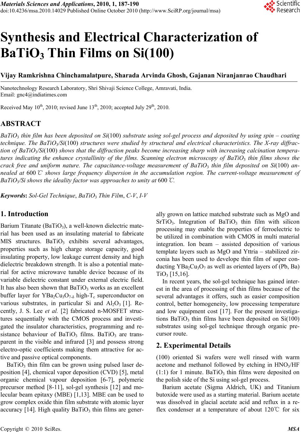
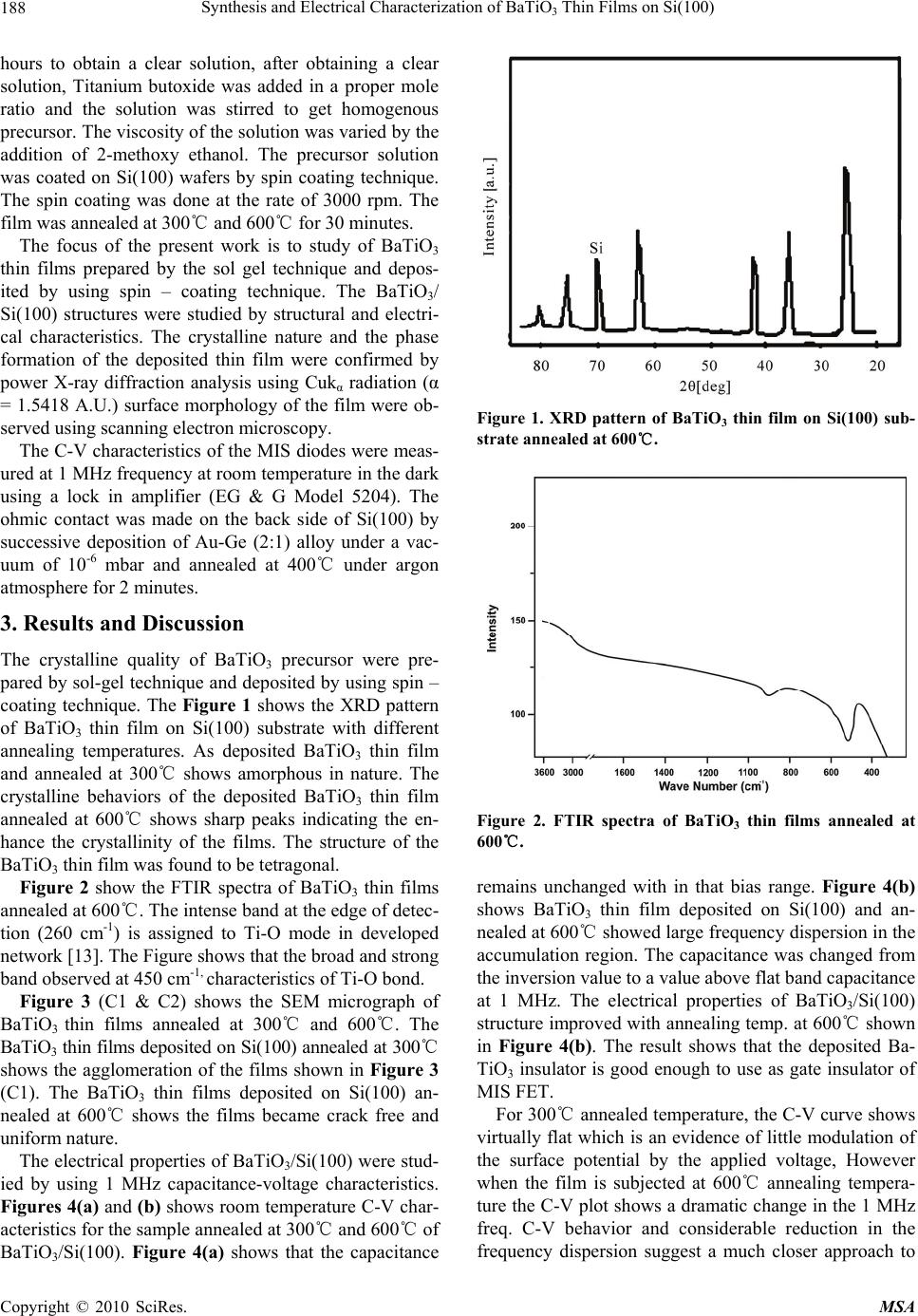
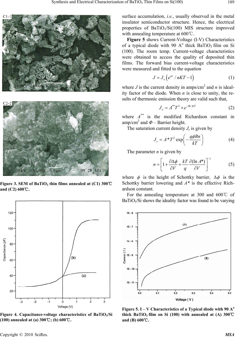
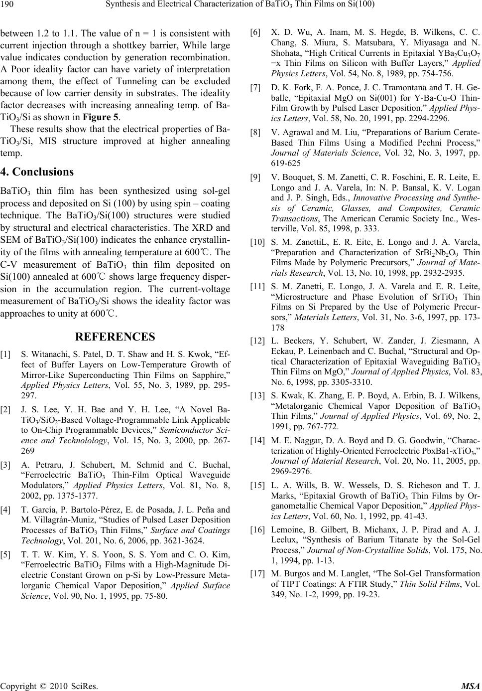
 Materials Sciences and Applications, 2010, 1, 187-190 doi:10.4236/msa.2010.14029 Published Online October 2010 (http://www.SciRP.org/journal/msa) Copyright © 2010 SciRes. MSA 187 Synthesis and Electrical Characterization of BaTiO3 Thin Films on Si(100) Vijay Ramkrishna Chinchamalatpure, Sharada Arvinda Ghosh, Gajanan Niranjanrao Chaudhari Nanotechnology Research Laboratory, Shri Shivaji Science College, Amravati, India. Email: gnc4@indiatimes.com Received May 10th, 2010; revised June 13th, 2010; accepted July 29th, 2010. ABSTRACT BaTiO3 thin film has been deposited on Si(100) substrate using sol-gel process and deposited by using spin – coating technique. The BaTiO3/Si(100) structures were studied by structural and electrical characteristics. The X-ray diffrac- tion of BaTiO3/Si(100) shows that the diffraction peaks become increasing sharp with increasing calcination tempera- tures indicating the enhance crystallinity of the films. Scanning electron microscopy of BaTiO3 thin films shows the crack free and uniform nature. The capacitance-voltage measurement of BaTiO3 thin film deposited on Si(100) an- nealed at 600 ℃ shows large frequency dispersion in the accumulation region. The current-voltage measurement of BaTiO3/Si shows the ideality factor was approaches to unity at 600 ℃ . Keywords: Sol-Gel Technique, BaTiO3 Thin Film, C-V, I-V 1. Introduction Barium Titanate (BaTiO3), a well-known dielectric mate- rial has been used as an insulating material to fabricate MIS structures. BaTiO3 exhibits several advantages, properties such as high charge storage capacity, good insulating property, low leakage current density and high dielectric breakdown strength. It is also a potential mate- rial for active microwave tunable device because of its variable dielectric constant under external electric field. It has also been shown that BaTiO3 works as an excellent buffer layer for YBa2Cu3O7-δ high-Tc superconductor on various substrates, in particular Si and Al2O3 [1]. Re- cently, J. S. Lee et al. [2] fabricated n-MOSFET struc- tures sequentially with the CMOS process and investi- gated the insulator characteristics, programming and re- sistance behaviour of BaTiO3 films. BaTiO3 are trans- parent in the visible and infrared [3] and possess strong electro-optic coefficients making them attractive for ac- tive and passive optical components. BaTiO3 thin film can be grown using pulsed laser de- position [4], chemical vapor deposition (CVD) [5], metal organic chemical vapour deposition [6-7], polymeric precursor method [8-11], sol-gel synthesis [12] and mo- lecular beam epitaxy (MBE) [1,13]. MBE can be used to grow complex oxide thin film substrate with atomic layer accuracy [14]. High quality BaTiO3 thin films are gener- ally grown on lattice matched substrate such as MgO and SrTiO3. Integration of BaTiO3 thin film with silicon processing may enable the properties of ferroelectric to be utilized in combination with CMOS in multi material integration. Ion beam – assisted deposition of various template layers such as MgO and Yttria – stabilized zir- conia has been used to develope thin film of super con- ducting YBa2Cu3O7 as well as oriented layers of (Pb, Ba) TiO3 [15,16]. In recent years, the sol-gel technique has gained inter- est in the area of processing of thin films because of the several advantages it offers, such as easier composition control, better homogeneity, low processing temperature and low equipment cost [17]. For the present investiga- tions BaTiO3 thin films have been deposited on Si(100) substrates using sol-gel technique through organic pre- cursor route. 2. Experimental Details (100) oriented Si wafers were well rinsed with warm acetone and methanol followed by etching in HNO3/HF (1:1) for 1 minute. BaTiO3 thin films were deposited on the polish side of the Si using sol-gel process. Barium acetate (Sigma Aldrich, UK) and Titanium butoxide were used as a starting material. Barium acetate was dissolved in glacial acetate acid and reflux in a re- flex condenser at a temperature of about 120℃ for six  Synthesis and Electrical Characterization of BaTiO3 Thin Films on Si(100) Copyright © 2010 SciRes. MSA 188 hours to obtain a clear solution, after obtaining a clear solution, Titanium butoxide was added in a proper mole ratio and the solution was stirred to get homogenous precursor. The viscosity of the solution was varied by the addition of 2-methoxy ethanol. The precursor solution was coated on Si(100) wafers by spin coating technique. The spin coating was done at the rate of 3000 rpm. The film was annealed at 300℃ and 600℃ for 30 minutes. The focus of the present work is to study of BaTiO3 thin films prepared by the sol gel technique and depos- ited by using spin – coating technique. The BaTiO3/ Si(100) structures were studied by structural and electri- cal characteristics. The crystalline nature and the phase formation of the deposited thin film were confirmed by power X-ray diffraction analysis using Cukα radiation (α = 1.5418 A.U.) surface morphology of the film were ob- served using scanning electron microscopy. The C-V characteristics of the MIS diodes were meas- ured at 1 MHz frequency at room temperature in the dark using a lock in amplifier (EG & G Model 5204). The ohmic contact was made on the back side of Si(100) by successive deposition of Au-Ge (2:1) alloy under a vac- uum of 10-6 mbar and annealed at 400℃ under argon atmosphere for 2 minutes. 3. Results and Discussion The crystalline quality of BaTiO3 precursor were pre- pared by sol-gel technique and deposited by using spin – coating technique. The Figure 1 shows the XRD pattern of BaTiO3 thin film on Si(100) substrate with different annealing temperatures. As deposited BaTiO3 thin film and annealed at 300℃ shows amorphous in nature. The crystalline behaviors of the deposited BaTiO3 thin film annealed at 600℃ shows sharp peaks indicating the en- hance the crystallinity of the films. The structure of the BaTiO3 thin film was found to be tetragonal. Figure 2 show the FTIR spectra of BaTiO3 thin films annealed at 600℃. The intense band at the edge of detec- tion (260 cm-1) is assigned to Ti-O mode in developed network [13]. The Figure shows that the broad and strong band observed at 450 cm-1, characteristics of Ti-O bond. Figure 3 (C1 & C2) shows the SEM micrograph of BaTiO3 thin films annealed at 300℃ and 600℃. The BaTiO3 thin films deposited on Si(100) annealed at 300℃ shows the agglomeration of the films shown in Figure 3 (C1). The BaTiO3 thin films deposited on Si(100) an- nealed at 600℃ shows the films became crack free and uniform nature. The electrical properties of BaTiO3/Si(100) were stud- ied by using 1 MHz capacitance-voltage characteristics. Figures 4(a) and (b) shows room temperature C-V char- acteristics for the sample annealed at 300℃ and 600℃ of BaTiO3/Si(100). Figure 4(a) shows that the capacitance Figure 1. XRD pattern of BaTiO3 thin film on Si(100) sub- strate annealed at 600℃. Figure 2. FTIR spectra of BaTiO3 thin films annealed at 600℃. remains unchanged with in that bias range. Figure 4(b) shows BaTiO3 thin film deposited on Si(100) and an- nealed at 600℃ showed large frequency dispersion in the accumulation region. The capacitance was changed from the inversion value to a value above flat band capacitance at 1 MHz. The electrical properties of BaTiO3/Si(100) structure improved with annealing temp. at 600℃ shown in Figure 4(b). The result shows that the deposited Ba- TiO3 insulator is good enough to use as gate insulator of MIS FET. For 300℃ annealed temperature, the C-V curve shows virtually flat which is an evidence of little modulation of the surface potential by the applied voltage, However when the film is subjected at 600℃ annealing tempera- ture the C-V plot shows a dramatic change in the 1 MHz freq. C-V behavior and considerable reduction in the frequency dispersion suggest a much closer approach to  Synthesis and Electrical Characterization of BaTiO3 Thin Films on Si(100) Copyright © 2010 SciRes. MSA 189 Figure 3. SEM of BaTiO3 thin films annealed at (C1) 300℃ and (C2) 600℃. Figure 4. Capacitance-voltage characteristics of BaTiO3/Si (100) annealed at (a) 300℃; (b) 600℃. surface accumulation, i.e., usually observed in the metal insulator semiconductor structure. Hence, the electrical properties of BaTiO3/Si(100) MIS structure improved with annealing temperature at 600℃. Figure 5 shows Current-Voltage (I-V) Characteristics of a typical diode with 90 Ao thick BaTiO3 film on Si (100). The room temp. Current-voltage characteristics were obtained to access the quality of deposited thin films. The forward bias current-voltage characteristics were measured and fitted to the equation /1 av o JJe nKT (1) where J is the current density in amps/cm2 and n is ideal- ity factor of the diode. When n is close to unity, the re- sults of thermonic emission theory are valid such that, ** 2/ K T o JATe (2) where A** is the modified Richardson constant in amp/cm2 and Φ – Barrier height. The saturation current density Js is given by 2 *exp s qBn JAT kT (4) The parameter n is given by 1 (ln *) 1kT A nVq V (5) where is the height of Schottky barrier, is the Schottky barrier lowering and A* is the effective Rich- ardson constant. For the annealing temperature at 300 and 600℃ of BaTiO3/Si shows the ideality factor was found to be varying Figure 5. I – V Characteristics of a Typical diode with 90 Ao thick BaTiO3 film on Si (100) with annealed at (A) 300℃ and (B) 600℃.  Synthesis and Electrical Characterization of BaTiO3 Thin Films on Si(100) Copyright © 2010 SciRes. MSA 190 between 1.2 to 1.1. The value of n = 1 is consistent with current injection through a shottkey barrier, While large value indicates conduction by generation recombination. A Poor ideality factor can have variety of interpretation among them, the effect of Tunneling can be excluded because of low carrier density in substrates. The ideality factor decreases with increasing annealing temp. of Ba- TiO3/Si as shown in Figure 5. These results show that the electrical properties of Ba- TiO3/Si, MIS structure improved at higher annealing temp. 4. Conclusions BaTiO3 thin film has been synthesized using sol-gel process and deposited on Si (100) by using spin – coating technique. The BaTiO3/Si(100) structures were studied by structural and electrical characteristics. The XRD and SEM of BaTiO3/Si(100) indicates the enhance crystallin- ity of the films with annealing temperature at 600℃. The C-V measurement of BaTiO3 thin film deposited on Si(100) annealed at 600℃ shows large frequency disper- sion in the accumulation region. The current-voltage measurement of BaTiO3/Si shows the ideality factor was approaches to unity at 600℃. REFERENCES [1] S. Witanachi, S. Patel, D. T. Shaw and H. S. Kwok, “Ef- fect of Buffer Layers on Low-Temperature Growth of Mirror-Like Superconducting Thin Films on Sapphire,” Applied Physics Letters, Vol. 55, No. 3, 1989, pp. 295- 297. [2] J. S. Lee, Y. H. Bae and Y. H. Lee, “A Novel Ba- TiO3/SiO2-Based Voltage-Programmable Link Applicable to On-Chip Programmable Devices,” Semiconductor Sci- ence and Technolology, Vol. 15, No. 3, 2000, pp. 267- 269 [3] A. Petraru, J. Schubert, M. Schmid and C. Buchal, “Ferroelectric BaTiO3 Thin-Film Optical Waveguide Modulators,” Applied Physics Letters, Vol. 81, No. 8, 2002, pp. 1375-1377. [4] T. García, P. Bartolo-Pérez, E. de Posada, J. L. Peña and M. Villagrán-Muniz, “Studies of Pulsed Laser Deposition Processes of BaTiO3 Thin Films,” Surface and Coatings Technology, Vol. 201, No. 6, 2006, pp. 3621-3624. [5] T. T. W. Kim, Y. S. Yoon, S. S. Yom and C. O. Kim, “Ferroelectric BaTiO3 Films with a High-Magnitude Di- electric Constant Grown on p-Si by Low-Pressure Meta- lorganic Chemical Vapor Deposition,” Applied Surface Science, Vol. 90, No. 1, 1995, pp. 75-80. [6] X. D. Wu, A. Inam, M. S. Hegde, B. Wilkens, C. C. Chang, S. Miura, S. Matsubara, Y. Miyasaga and N. Shohata, “High Critical Currents in Epitaxial YBa2Cu3O7 −x Thin Films on Silicon with Buffer Layers,” Applied Physics Letters, Vol. 54, No. 8, 1989, pp. 754-756. [7] D. K. Fork, F. A. Ponce, J. C. Tramontana and T. H. Ge- balle, “Epitaxial MgO on Si(001) for Y-Ba-Cu-O Thin- Film Growth by Pulsed Laser Deposition,” Applied Phys- ics Letters, Vol. 58, No. 20, 1991, pp. 2294-2296. [8] V. Agrawal and M. Liu, “Preparations of Barium Cerate- Based Thin Films Using a Modified Pechni Process,” Journal of Materials Science, Vol. 32, No. 3, 1997, pp. 619-625 [9] V. Bouquet, S. M. Zanetti, C. R. Foschini, E. R. Leite, E. Longo and J. A. Varela, In: N. P. Bansal, K. V. Logan and J. P. Singh, Eds., Innovative Processing and Synthe- sis of Ceramic, Glasses, and Composites, Ceramic Transactions, The American Ceramic Society Inc., Wes- terville, Vol. 85, 1998, p. 333. [10] S. M. ZanettiL, E. R. Eite, E. Longo and J. A. Varela, “Preparation and Characterization of SrBi2Nb2O9 Thin Films Made by Polymeric Precursors,” Journal of Mate- rials Research, Vol. 13, No. 10, 1998, pp. 2932-2935. [11] S. M. Zanetti, E. Longo, J. A. Varela and E. R. Leite, “Microstructure and Phase Evolution of SrTiO3 Thin Films on Si Prepared by the Use of Polymeric Precur- sors,” Materials Letters, Vol. 31, No. 3-6, 1997, pp. 173- 178 [12] L. Beckers, Y. Schubert, W. Zander, J. Ziesmann, A Eckau, P. Leinenbach and C. Buchal, “Structural and Op- tical Characterization of Epitaxial Waveguiding BaTiO3 Thin Films on MgO,” Journal of Applied Physics, Vol. 83, No. 6, 1998, pp. 3305-3310. [13] S. Kwak, K. Zhang, E. P. Boyd, A. Erbin, B. J. Wilkens, “Metalorganic Chemical Vapor Deposition of BaTiO3 Thin Films,” Journal of Applied Physics, Vol. 69, No. 2, 1991, pp. 767-772. [14] M. E. Naggar, D. A. Boyd and D. G. Goodwin, “Charac- terization of Highly-Oriented Ferroelectric PbxBa1-xTiO3,” Journal of Material Research, Vol. 20, No. 11, 2005, pp. 2969-2976. [15] L. A. Wills, B. W. Wessels, D. S. Richeson and T. J. Marks, “Epitaxial Growth of BaTiO3 Thin Films by Or- ganometallic Chemical Vapor Deposition,” Applied Phys- ics Letters, Vol. 60, No. 1, 1992, pp. 41-43. [16] Lemoine, B. Gilbert, B. Michanx, J. P. Pirad and A. J. Leclux, “Synthesis of Barium Titanate by the Sol-Gel Process,” Journal of Non-Crystalline Solids, Vol. 175, No. 1, 1994, pp. 1-13. [17] M. Burgos and M. Langlet, “The Sol-Gel Transformation of TIPT Coatings: A FTIR Study,” Thin Solid Films, Vol. 349, No. 1-2, 1999, pp. 19-23. |

