Circuits and Systems
Vol.07 No.09(2016), Article ID:68709,12 pages
10.4236/cs.2016.79209
A Novel Multilevel Inverter Employing Additive and Subtractive Topology
V. Prasannamoorthy1, P. Sundaramoorthi2, Merin Jacob2
1Government College of Technology, Coimbatore, Tamil Nadu, India
2Department of Electrical and Electronics Engineering, Nehru College of Engineering and Research Centre, Thrissur, India

Copyright © 2016 by authors and Scientific Research Publishing Inc.
This work is licensed under the Creative Commons Attribution International License (CC BY).
http://creativecommons.org/licenses/by/4.0/


Received 20 April 2016; accepted 10 May 2016; published 20 July 2016
ABSTRACT
As the demand for high voltage, high power inverters are increasing and there is a problem of connecting a power semiconductor switch directly to a high voltage network. As a part of this the multilevel inverters had been introduced. As a part of this, several researches had been done for the development of multilevel inverters. The commercially available and extensively studied topologies for multilevel voltage output are Neutral Point Clamped (NPC), Cascaded Half Bridge (CHB) and Flying Capacitor (FC) converters. However, with these existing topologies, there is a significant increase in the number of power switches and passive components. Thus it leads to more complex control circuitry and overall cost of the system increase with increase in the output levels. In this paper, a novel multilevel inverter is proposed in which it employs additive and subtractive topology to get higher output levels. This approach significantly reduces the number of power switches needed as compared to existing topology. The present developed multilevel inverter can generate only five voltage levels. With this proposed topology the multilevel inverter can be modified to nine-level inverter. Moreover modified hybrid multicarrier Pulse Width Modulation (PWM) technique can be implemented in the proposed multilevel inverter in order to obtain uniform switch utilization and lower THD. An appropriate modulation scheme is presented and also the proposed concept is analyzed through simulation studies.
Keywords:
Multilevel Inverter (MLI), Pulse Width Modulation (PWM), Multicarrier PWM Scheme, Additive and Subtractive Topology, Total Harmonic Distortion (THD)

1. Introduction
In the recent technologies, multilevel voltage source inverters have emerged as a viable solution for the conversion of Direct Current (DC) to Alternate Current (AC) applications. As the name defined Multilevel Inverter (MLI) is used to generate different voltage levels, i.e., voltage levels greater than three or more. MLI is defined as a linkage structure of multiple input DC sources and power semiconductor devices to generate a staircase waveform. As compared to the conventional inverters, voltage stress experienced by the power switches is much lower in the case of MLIs. In addition to this, a better harmonic profile wave form can be obtained from MLIs as compared to two-level waveform conventional inverters. MLIs have other advantages also such as reduced dv/dt stress on load and possibility of fault tolerant operation. For low power applications, the researchers are exploring the implementation of MLIs. By increasing the number of levels we can enhance the quality of multilevel waveform. But however, it adversely increases the number of power semiconductor devices and accompanying gate driver circuits. As a result of this the system complexity and cost gets increased and thus reduce the system reliability and efficiency. Therefore in order to achieve high resolution waveform, practical considerations necessitate reduction in the number of switches and gate driver circuits.
The topologies which have been extensively studied and available for multilevel voltage output are Neutral Point Clamped (NPC), Cascaded H-Bridge (CHB) and Flying Capacitor (FC) converters. With the increase in the number of output levels, there is a significant increase in the number of power switches and overall cost of the system. Therefore researchers through various approaches focus to reduce the component count in multilevel topologies. These approaches can be broadly classified into mainly three categories such as topological changes use of asymmetric sources, combination of topological changes and asymmetric source configurations. In Section 3, we are dealing with a topology of switched DC source topology [1] . In this topology the DC sources are alternatively connected in opposite polarities through power switches. Here we are using multiple input DC voltages and these voltage levels can be combined in to all additive values. This topology is explained with the help of a five-level inverter. This topology has several disadvantages. So in order to rectify the disadvantages of Switched DC Source topology we are proposing a new topology known as additive and subtractive topology. A detailed study of this topology is done in this paper. In this topology the number of levels developed mainly depends upon the DC source arrangement. This approach significantly reduces the number of power switches and gate driver circuits needed as compared to the DC Source topology. The proposed topology is developed with a nine-level Multilevel Inverter. As a disadvantage with the existing DC Source topology it needs 10 switches and 4 DC sources in order to develop a nine-level inverter. But with the proposed topology it needs only 8 switches and 2 DC sources. Thus the proposed topology reduces the component count and Total Harmonic Distortion (THD). The detailed study of the proposed topology is done in this paper with a nine-level multilevel inverter [2] .
2. Switched Dc Source Topology
In this topology alternate DC sources are linked in opposite polarities via power switches. This topology shows similarity with the CHB topology in two ways such as it needs multiple isolated input DC voltages and input DC voltage levels are combined in to all additive values. The linkage structure in this topology can be obtained by connecting the higher potential terminal of the preceding source to the lower potential terminal of the succeeding source and vice versa via power switches. These power switches can be implemented using a transistor device such as MOSFET and IGBT with an antiparallel diode. The Switched DC Source topology is described with a single phase nine-level inverter as shown in Figure 1. Here in this topology, it consists of three pairs of active switches T1, T2, T3 and their complimentary switches ,
,  ,
,  with two input voltage sources E1 and E2.
The five voltage levels are obtained by the proper switching of these switches. With this topology we are generating five voltage levels such as +Vdc, −Vdc, +2Vdc, −2Vdc and zero for E1 = E2 = Vdc. The output voltage E1 is obtained when switches T1,  and
and  are ON. When switches T3,
  ,
,  are ON we get output voltage of E2. The output voltage (E1 + E2) is obtained by turning ON the switches T1,
  and T3. Thus correspondingly we get other output voltages such as −(E1 + E2), −E1 and E2. With this topology if we are stepping up five level to nine level it needs 4 DC sources and 10 switches. But if we are implementing a new topology known as “Additive and Subtractive” topology, we are able to generate nine level with 2 DC sources and 8 switches. Therefore with this topology we can reduce the component count to a maximum limit. The detailed study of this topology is further discussed in the next section.

Figure 1. Single phase nine-level inverter based on switched dc source topology.
3. Proposed Concept and Topology
Nowadays MLIs are becoming more popular due to reduced voltage stress across power switches and low THD output voltage wave form. However as level increases the device count also increases. So in order to obtain maximum number of levels in output waveform with limited number of components we are proposing a novel topology known as additive and subtractive topology. This paper presents a novel multilevel topology which is capable of obtaining all additive and subtractive combinations of input DC levels in the output waveform. Here the actual number of levels generated depends on the DC source arrangement. The DC sources and switches are arranged in such a manner that it is possible to obtain all possible combinations in the output, i.e., if “n” number of DC sources are present, then “4n” power switches are required to obtain all possible combinations. From this concept for the proposed topology total number of power switches required is “4n”.
3.1. Working Principle
The working principle of proposed topology is described with the help of a single phase nine-level inverter. Here it consists of two input asymmetric DC sources E1 and E2, such that E2 < E1 as shown in Figure 2. The DC source arrangement is chosen such that E1/E2 = 3. Therefore with this configuration it is able to generate nine output levels. The DC source can be arranged in several manners such that:
1) “Unary” arrangement will result if all the DC sources are equal, i.e.
 (1)
(1)
2) “Binary” arrangement will result if the DC sources make a geometric progression with a factor of “1/2”, i.e.
 (2)
(2)

Figure 2. Proposed single phase nine-level inverter.
4) “Trinary” arrangement will result if the DC sources make a geometric progression with a factor of “1/3”, i.e.
 (3)
(3)
3.2. Working States
The proposed topology is described with a nine-level inverter with two input DC sources as shown in Figure 2. Here the two sources are taken such that E2 < E1 and they can be arranged in unary, binary, or trinary. This arrangement of the DC sources decides the actual number of levels in the output. For example, by employing two sources E1 and E2 having equal values (E1 = E2 = EO), five output levels (viz. ±EO, ±2EO and 0) can be obtained (i.e. a five-level waveform in steps of EO). By employing a binary source configuration (with E1 = 2EO and E2 = EO), seven output levels (viz. ±EO, ±2EO, ±3EO and 0) can be synthesized (i.e. a seven-level waveform in steps of EO). Similarly, a trinary source configuration (with E1 = 3EO and E2 = EO) would synthesize voltage levels (±EO, ±2EO, ±3EO, ±4EO and 0) i.e. a nine-level waveform in steps of EO. Practically, we can obtain the desired source configuration in applications like renewable energy sources where separate DC sources are available and AC drives where multi-winding transformers are used. In this topology it has eight switches and three switches are needed to be ON simultaneously to obtain any desired voltage level.
3.3. Power Switch Configurations
The proposed inverter can be realized with self-commutating power switches like MOSFET’s and IGBT’s. It is also important to note that the switches at positions T2 and  are necessarily required to be “fully directional switches” otherwise their undesirable switching will take place. This is described with the help of Figure 3 where IGBT’s are shown at the places of T2 and
 . When an output level (E1 + E2) is required and switches
 , T3 and T1 are ON, then the anti-parallel diode of switch
  gets a forward biasing potential difference of E2. Thus it acts as ON switch, thereby short-circuiting the source E2. A similar phenomenon happens when switches T4,
  and
and  are ON in order to attain an output level of (E1 + E2). Under such conditions, the anti-parallel diode of T2 gets a forward-biasing potential difference equal to E2, thereby short-circuiting the source E2. Therefore, at both positions T2 and
 , fully directional switches having the capability of blocking voltages in both directions are to be used.
4. Modulation Scheme
For the multilevel inverter modulation control we can use either Multicarrier PWM or space vector modulation techniques [3] [4] . These techniques employ high switching frequency, thus causing extra switching losses. Apart from this, methods such as active harmonic elimination, Selective Harmonic Elimination (SHE) and fundamental frequency methods are low switching frequency methods. All the aforesaid methods can be used for the control of proposed structure. But here the control is demonstrated through low switching frequency multicarrier scheme [5] [6] . In a multicarrier PWM scheme, carrier signals are compared with the reference signal and the pulses so obtained are used for switching of device corresponding to the respective voltage levels [5] . However, in the proposed structure, various switches do not operate independent of each other. Therefore, the resultant signals from the comparison of carriers and reference cannot be directly fed to the switches. In Figure 4, the overall modulation strategy is demonstrated.
In the proposed modulation scheme, for all the carrier waveforms above the time-axis, the results of comparison

Figure 3. Proposed configuration for single phase nine-level inverter.
with the reference sine wave are “1” or “0”. For all the carrier waves below the time-axis, the results of comparison with the reference sine wave are “0” or “−1”. Here we are implementing a new modulation technique known as multi carrier pulse width modulation technique [7] . With this technique uniform switch utilization and even power distribution can be achieved. This mode of control is given in Figure 5 and the corresponding waveforms are shown in Figure 6. The signals so obtained are aggregated so as to synthesize an aggregated signal “As”. The aggregated signal “As” has same number of levels as desired in the output waveform and it is shown in Figure 7.
The switching signals for the switches are obtained from this aggregate signal. The switching signals thus obtained are known as D-states. Thus D-states are generated by combining it with switching pattern and saturation limits. Here it consists of a total of nine lookup tables as shown in Figure 8. In each lookup table D-States are generated by the combination of’ NOT’ and “AND” operations. The corresponding D-State switching scheme is shown in Figure 9, and the corresponding wave form is shown in Figure 10. The overall simulation model for the proposed system is shown in Figure 11 and it consists of voltage divider, pulse generation and multilevel inverter.

Figure 4. Proposed modulation scheme.

Figure 5. Proposed control technique.
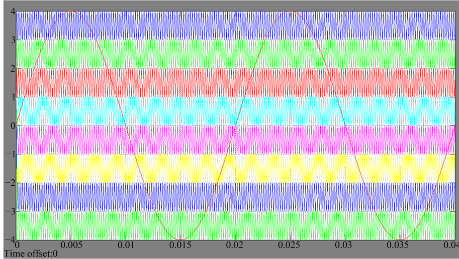
Figure 6. Resultant comparison waveform.

Figure 7. Proposed aggregated signal.

Figure 8. Lookup tables for nine voltage levels.
5. Simulation Results
Using MATLAB/Simulink the proposed structure is simulated to get nine-level output. The DC sources are taken

Figure 9. Proposed D-state switching scheme.

Figure 10. D-state switching wave form.
such that E1 = 12.5 V and E2 = 37.5 V. In the previous section modulation scheme is described and it is considered for inductive load. The inverter is operated in open loop mode. With this proposed topology it produces nine voltage levels and it is shown in Figure 12. The load voltage and its corresponding harmonic spectrum is shown in Figure 13. From this result it can be noticed that output voltage waveform has THD of 13.89%. With the proposed topology current output waveform and its corresponding harmonic spectrum are shown in Figure 14 and Figure 15 and it is noticed that load current waveform has THD of 2.97%.

Figure 11. Overall simulation model for nine- level inverter.

Figure 12. Single phase nine-level voltage output.
6. Conclusion
As MLIs are gaining interest, efforts are being directed towards reducing the device count for increased number of output levels. As a part of this, a new topology known as additive and subtractive topology had developed to reduce the device count. Instead of using cascaded inverter topology and switched DC source topology, the proposed topology is better because it has less control complexities, less cost and gives less percentage of THD. This topology can be effectively employed only for applications where isolated DC sources are available. On behalf of this, several surveys about MLIs had been conducted. Based upon these surveys a novel multilevel inverter can be developed which employs additive and subtractive topology. By implementing this topology, it

Figure 13. Harmonic spectrum of nine-level voltage output.

Figure 14. Load current waveform for nine-level voltage.

Figure 15. Harmonic spectrum for load current.
nullifies the drawbacks of switched DC source topology and thus improves the reliability. In addition to this hybrid PWM modulation technique can be applied for the uniform switch utilization and even power distribution.
Cite this paper
V. Prasannamoorthy,P. Sundaramoorthi,Merin Jacob, (2016) A Novel Multilevel Inverter Employing Additive and Subtractive Topology. Circuits and Systems,07,2425-2436. doi: 10.4236/cs.2016.79209
References
- 1. Gupta, K.K. and Jain, S. (2014) A Novel Multilevel Inverter Based on Switched DC Sources. IEEE Transactions on Industrial Electronics, 61, 3269-3278.
http://dx.doi.org/10.1109/TIE.2013.2282606 - 2. Gupta, K.K. and Jain, S. (2012) Topology for Multilevel Inverters to Attain Maximum Number of Levels from Given DC Sources. IET Power Electronics, 5, 435-446.
http://dx.doi.org/10.1049/iet-pel.2011.0178 - 3. Tolbert, L.M. and Habetler, T.G. (1999) Novel Multilevel Inverter Carrier-Based PWM Method. IEEE Transactions on Industry Applications, 35, 1098-1107.
http://dx.doi.org/10.1109/28.793371 - 4. Yao, W., Hu, H. and Lu, Z. (2008) Comparisons of Space-Vector Modulation and Carrier-Based Modulation of Multilevel Inverter. IEEE Transactions on Power Electronics, 23, 45-51.
http://dx.doi.org/10.1109/TPEL.2007.911865 - 5. Carrara, G., Gardella, S., Marchesoni, M., Salutari, R. and Sciutto, G. (1992) A New Multilevel PWM Method: A Theoretical Analysis. IEEE Transactions on Power Electronics, 7, 497-505.
http://dx.doi.org/10.1109/63.145137 - 6. Ozpineci, B., Tolbert, L.M. and Du, Z. (2004) Optimum Fuel Cell Utilization with Multilevel Inverters. 35th Annual IEEE Power Electronics Specialist’s Conference, Aachen, 20-25 June 2004, 4798-4802.
- 7. Sarkar, I. and Fernandes, B.G. (2014) Modified Hybrid Multi-Carrier PWM Technique for Cascaded H-Bridge Multilevel Inverter. 40th Annual Conference of the IEEE Industrial Electronics Society, IECON 2014, Dallas, 29 October-1 November 2014, 4318-4324.
http://dx.doi.org/10.1109/iecon.2014.7049152