Paper Menu >>
Journal Menu >>
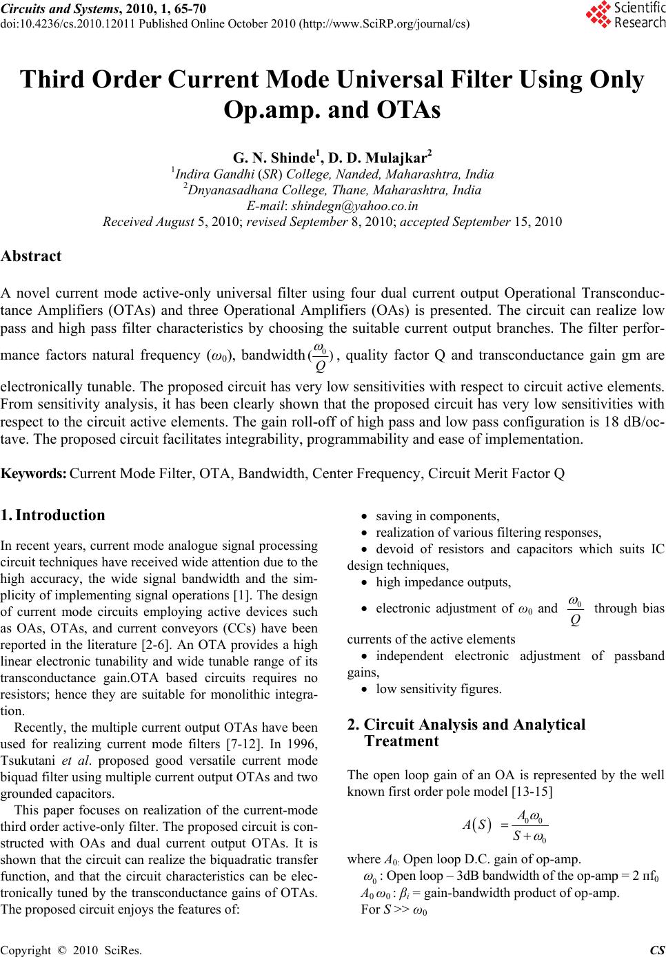 Circuits and S doi:10.4236/cs. Copyright © 2 Thir d Abstract A novel cur r tance Ampli pass and hi g mance facto r electronicall y From sensiti v respect to th e tave. The pr o Keywords: C 1. Introdu c In recent yea r circuit techni q high accurac y p licity of imp l of current m o as OAs, OT A reported in th linear electro n transconduct a resistors; hen c tion. Recently, t h used for real i Tsukutani et b iquad filter u grounded cap a This paper third order ac t structed with shown that th e function, and tronically tun e The proposed Sy stems, 2010 2010.12011 Pu b 2 010 SciRes. d Orde r Received r ent mode a c fiers (OTAs ) g h pass filter r s natural fr e y tunable. T h v ity analysis e circuit acti v o posed circu i C urrent Mod e c tion r s, current mo d q ues have rece y , the wide si g l ementing sig n o de circuits e m A s, and curren t e literature [2 - n ic tunability a a nce gain.OT A c e they are s u h e multiple c u i zing current m al. proposed u sing multiple a citors. focuses on re t ive-only filte r OAs and du a e circuit can r e that the circu e d by the tran s circuit enjoys , 1, 65-70 b lished Online O r Curr e O 1 I ndira Ga n 2 Dnyan a August 5, 201 c tive-only u n ) and three O characteristi e quency (ω 0 ) h e proposed c , it has been v e elements. i t facilitates i n e Filter, OTA d e analogue si ived wide att e g nal bandwid t n al operations m ploying acti v t conveyors ( C - 6]. An OTA p a nd wide tun a A based circ u u itable for mo n u rrent output O m ode filters [ good versatil e current outpu t alization of t h r . The propose a l current out p e alize the biq u it characterist i s conductance the features o O ctobe r 2010 ( h e nt Mo d O p.am p G. N. Shind n dhi (SR) Col l sadhana Coll e E-mail: s hi n 0; revised Se p n iversal filter O perational A c s by choosi ) , bandwidth ( c ircuit has v e clearly sho w The gain rol n tegrability, p , Bandwidth, gnal processi n e ntion due to t h t h and the si m [1]. The desi g v e devices su c C Cs) have be e p rovides a hi g a ble range of i u its requires n n olithic integ r a O TAs have be e 7-12]. In 199 6 e current mo d t OTAs and t w h e curren t -mo d d circuit is co n p ut OTAs. It u adratic trans fe i cs can be ele c gains of OT A f: h ttp://www.Sci R d e Uni v p . and O d e 1 , D. D. M u l ege, Nanded, M e ge, Thane, Ma n degn@yaho o p tembe r 8, 201 using four d A mplifiers ( O ng the suita b 0 ( ) Q , qualit y e ry low sensi t w n that the p r l-off of high p rogrammab i Center Freq u n g h e m - g n c h e n g h i ts n o a - e n 6 , d e w o d e n - is fe r c - A s. s a r e d e design h i e l curren t i n gains, l o 2. Ci r Tr e The o p known where A 0 : A 0 ω For S R P.org/journal/c s v ersal F O TAs u lajkar 2 M aharashtra, a harashtra, I n o .co.in 0; accepted S e d ual current o O As) is prese n b le current o u y factor Q a n t ivities with r r oposed circ u pass and lo w i lity and eas e u ency, Circu i a ving in comp o e alization of v a e void of resis techniques, i gh impedanc e l ectronic adju s t s of the active n dependent e l o w sensitivity f r cuit Anal ys e atment p en loop gain o first order po l A A 0: Open loop Open loop – 3 0 : β i = gain- ba S >> ω 0 s ) F ilter U s India n dia e ptembe r 15, 2 o utput Oper a n ted. The ci r u tput branch e n d transcond u r espect to cir u it has very l o w pass confi g e of impleme n i t Merit Fact o o nents, a rious filterin g tors and cap a e outputs, s tment of ω 0 a elements l ectronic adj u f igures. s is and An a o f an OA is r e l e model [13-1 0 0 A A SS D.C. gain of o dB bandwidth a ndwidth p rod u s ing O n 2 010 a tional Trans c r cuit can rea l e s. The filte r u ctance gain cuit active e l o w sensitivit i g uration is 1 8 n tation. o r Q g responses, a citors which a nd 0 Q thro u u stment of p a l y tical e presented by 5] 0 0 o p-amp. of the op-am p u ct of op-amp . CS n ly c onduc- l ize low r perfor- gm are l ements. i es with 8 dB/oc- suits IC u gh bias p assband the well p = 2 пf 0 .  G. N. SHINDE ET AL. Copyright © 2010 SciRes. CS 66 0i 0 (i1,2,3,) A AS SS This model of OA is valid from a few kHz to few hundred kHz. In this frequency range, OTA works as an ideal device. The OTA is characterized by the port-rela- tion IO = gm (V+ - V-) where, gm is transconductance of OTA. In the dual cur- rent output OTA, the plus current output has a positive polarity, and the minus current output has a negative polarity. The analysis gives the current transfer function T = [I out / I in] as follows: T(S) = 2 01122212 3233123 2 01122 2 3 1232331 3 3 2 )(() ())( mbmb mbmbmbmb mama mamamama gggSg gg g SS SSggSg gg (1) The circuit was designed using coefficient matching technique. i.e., by comparing these transfer functions with general third order transfer functions is given by, T(S) = 00 32 210 32 3 22 0 11 (1 )(1 ) SSS SS S QQ (2) Comparing Equations (1) with (2) we get, 0 31 323 0 ma ma g g 0 12 212 0 1 (1 ) ma ma ma gg gQ (3) 212323 0 0 1 (1 ) mb mb ma gg Qg 0 3 0 mb ma g g And 3 0 0 mb ma g g It is found from above equations that circuit parame- ters ω0, Q; α0 can independently set and electronically tuned adjusting the transconductance gains of the OTAs. If 0ma g ,1 , 2 and 3 are given, the parameter ω0 can be set by 2ma g . The parameters Q and α3 can be set by 1ma g and 0mb g respectively. It seems that the values of Q and α3 are also limited by the dynamic ranges of the OA and OTA. From (1), it can be seen that: 1) The low pass transfer function can be realized with 00 mb g 112 2mb mb gg and 212 323mb mb gg 2) The high pass transfer function can be realized with 30 mb g 112 2mb mb gg and 212 323mb mb gg 3) The band pass transfer function can be realized with 30 0 mb mb gg 112 2mb mb gg The high pass and low pass transfer functions obtained are as follows, 3 0 32 011 22212 3233123 () HP mama mamamama S TgS ggSggSg 3 32 01122212 3233123 () LP mama mamamama TgS ggSggSg The realization of the other transfer functions invariably requires matching the conditions in terms of the tran- sconductance gains of the OTAs and the gain-bandwidth products of the OAs. The transconductance gains of the OTAs to realize the desired characteristics are obtained from (3) as 3 0123 3 0 ma ma gg 2 000 2 12 123 1 {1 } ma ma g gQ 00 22 1 11 1 1 ma ma ma gg gQ where ω0, Q, , , and should be given in advance. Methods of implementing a dual current output OTA have been discussed previously (Ramirez-Angulo et al. 1992, Wu 1994). 3. Circuit Diagram The diagram was shown in Figure 1. 4. Circuit Description The proposed circuit is built with four dual current out- put OTAs and three OAs is as shown in Figure (1). The V+ terminal of first OTA and V-terminal of all other OTAs are grounded. Output terminal of first OTA carry- ing positive polarity current is fed to inverting terminal of first OA. Its output is fed to inverting terminal of 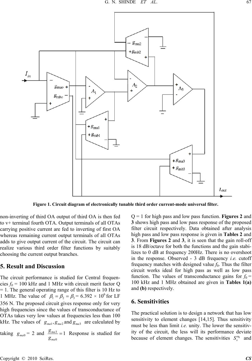 G. N. SHINDE ET AL. 67 Copyright © 2010 SciRes. CS Figure 1. Circuit diagram of electronically tunable third order current-mode universal filter. non-inverting of third OA output of third OA is then fed to v+ terminal fourth OTA. Output terminals of all OTAs carrying positive current are fed to inverting of first OA whereas remaining current output terminals of all OTAs adds to give output current of the circuit. The circuit can realize various third order filter functions by suitably choosing the current output branches. 5. Result and Discussion The circuit performance is studied for Central frequen- cies f0 = 100 kHz and 1 MHz with circuit merit factor Q = 1. The general operating range of this filter is 10 Hz to 1 MHz. The value of 123 = 6.392 × 10⁶ for LF 356 N. The proposed circuit gives response only for very high frequencies since the values of transconductance of OTAs takes very low values at frequencies less than 100 kHz. The values of 12 , ma ma g gand 3ma g are calculated by taking 0ma g = 2 and 3 0 1 ma ma g g Response is studied for Q = 1 for high pass and low pass function. Figures 2 and 3 shows high pass and low pass response of the proposed filter circuit respectively. Data obtained after analysis high pass and low pass response is given in Tables 2 and 3. From Figures 2 and 3, it is seen that the gain roll-off is 18 dB/octave for both the functions and the gain stabi- lizes to 0 dB at frequency 200Hz. There is no overshoot in the response. Observed - 3 dB frequency i.e. cutoff frequency matches with designed value f0. Thus the filter circuit works ideal for high pass as well as low pass function. The values of transconductance gains for f0 = 100 kHz and 1 MHz obtained are given in Tables 1(a) and (b) respectively. 6. Sensitivities The practical solution is to design a network that has low sensitivity to element changes [14,15]. Thus sensitivity must be less than limit i.e. unity. The lower the sensitiv- ity of the circuit, the less will its performance deviate because of element changes. The sensitivities 0 x S and 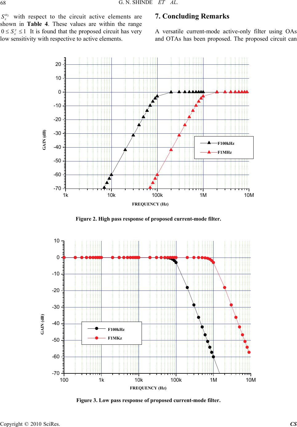 G. N. SHINDE ET AL. Copyright © 2010 SciRes. CS 68 3 x S with respect to the circuit active elements are shown in Table 4. These values are within the range 01 y x S It is found that the proposed circuit has very low sensitivity with respective to active elements. 7. Concluding Remarks A versatile current-mode active-only filter using OAs and OTAs has been proposed. The proposed circuit can 1k10k 100k1M10M -70 -60 -50 -40 -30 -20 -10 0 10 20 F100kHz F1MHz GAIN(dB) FREQUENCY(Hz) Figure 2. High pass response of proposed current-mode filter. 1001k10k 100k1M10M -70 -60 -50 -40 -30 -20 -10 0 10 F100kHz F1MKz GAIN(dB) FREQUENCY(Hz) Figure 3. Low pass response of proposed current-mode filter. FREQUENCY (Hz) GAIN (dB) F100kHz F1MHz FREQUENCY (Hz) F100kHz F1MKz GAIN (dB) 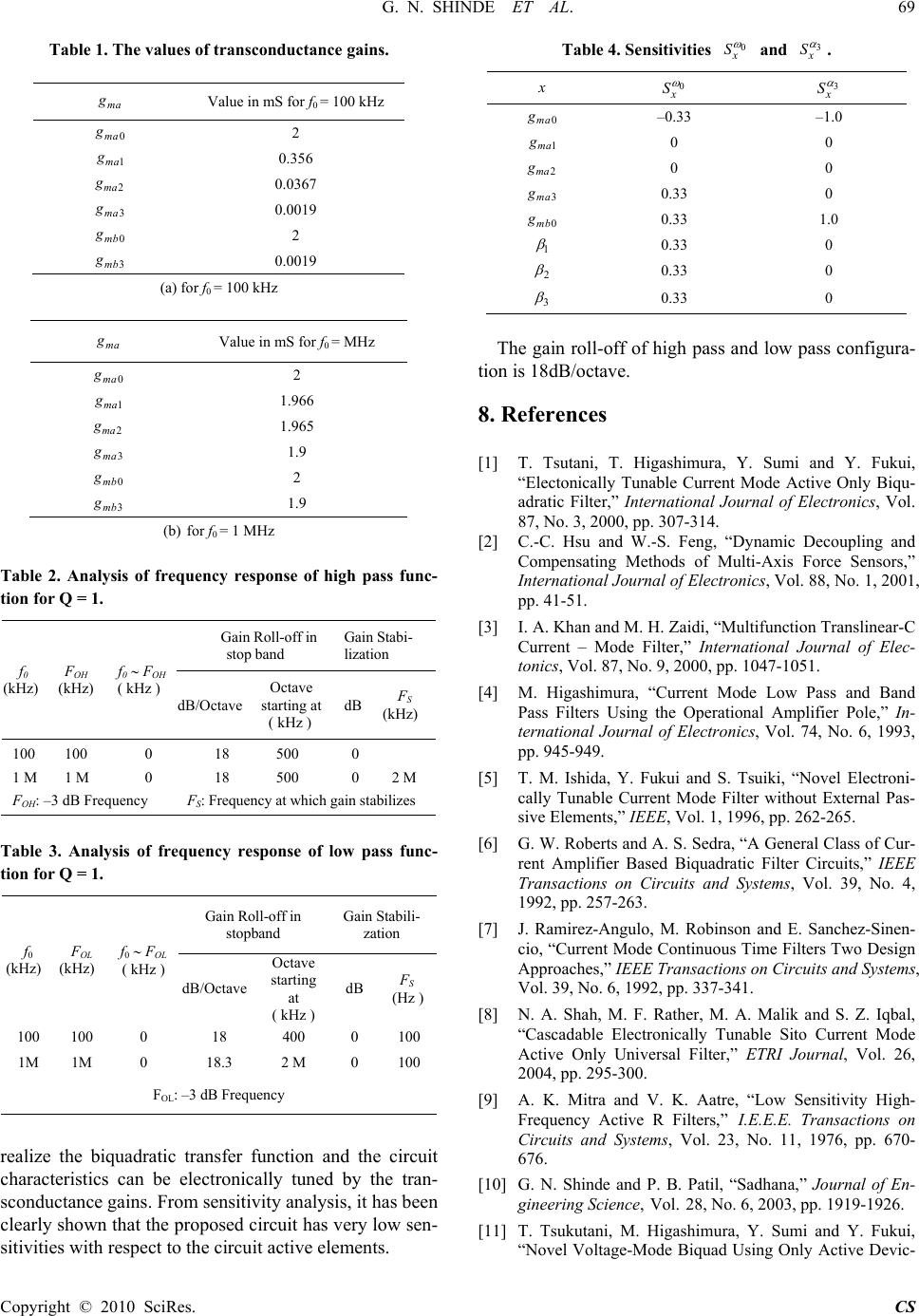 G. N. SHINDE ET AL. 69 Copyright © 2010 SciRes. CS Table 1. The values of transconductance gains. ma g Value in mS for f0 = 100 kHz 0ma g 2 1ma g 0.356 2ma g 0.0367 3ma g 0.0019 0mb g 2 3mb g 0.0019 (a) for f0 = 100 kHz ma g Value in mS for f0 = MHz 0ma g 2 1ma g 1.966 2ma g 1.965 3ma g 1.9 0mb g 2 3mb g 1.9 (b) for f0 = 1 MHz Table 2. Analysis of frequency response of high pass func- tion for Q = 1. f0 (kHz) FOH (kHz) f0 FOH ( kHz ) Gain Roll-off in stop band Gain Stabi- lization dB/Octave Octave starting at ( kHz ) dB FS (kHz) 100 100 0 18 500 0 1 M 1 M 0 18 500 0 2 M FOH: –3 dB Frequency FS: Frequency at which gain stabilizes Table 3. Analysis of frequency response of low pass func- tion for Q = 1. f0 (kHz) FOL (kHz) f0 FOL ( kHz ) Gain Roll-off in stopband Gain Stabili- zation dB/Octave Octave starting at ( kHz ) dB FS (Hz ) 100 100 0 18 400 0 100 1M 1M 0 18.3 2 M 0 100 FOL: –3 dB Frequency realize the biquadratic transfer function and the circuit characteristics can be electronically tuned by the tran- sconductance gains. From sensitivity analysis, it has been clearly shown that the proposed circuit has very low sen- sitivities with respect to the circuit active elements. Table 4. Sensitivities 0 x S and 3 x S . The gain roll-off of high pass and low pass configura- tion is 18dB/octave. 8. References [1] T. Tsutani, T. Higashimura, Y. Sumi and Y. Fukui, “Electonically Tunable Current Mode Active Only Biqu- adratic Filter,” International Journal of Electronics, Vol. 87, No. 3, 2000, pp. 307-314. [2] C.-C. Hsu and W.-S. Feng, “Dynamic Decoupling and Compensating Methods of Multi-Axis Force Sensors,” International Journal of Electronics, Vol. 88, No. 1, 2001, pp. 41-51. [3] I. A. Khan and M. H. Zaidi, “Multifunction Translinear-C Current – Mode Filter,” International Journal of Elec- tonics, Vol. 87, No. 9, 2000, pp. 1047-1051. [4] M. Higashimura, “Current Mode Low Pass and Band Pass Filters Using the Operational Amplifier Pole,” In- ternational Journal of Electronics, Vol. 74, No. 6, 1993, pp. 945-949. [5] T. M. Ishida, Y. Fukui and S. Tsuiki, “Novel Electroni- cally Tunable Current Mode Filter without External Pas- sive Elements,” IEEE, Vol. 1, 1996, pp. 262-265. [6] G. W. Roberts and A. S. Sedra, “A General Class of Cur- rent Amplifier Based Biquadratic Filter Circuits,” IEEE Transactions on Circuits and Systems, Vol. 39, No. 4, 1992, pp. 257-263. [7] J. Ramirez-Angulo, M. Robinson and E. Sanchez-Sinen- cio, “Current Mode Continuous Time Filters Two Design Approaches,” IEEE Transactions on Circuits and Systems, Vol. 39, No. 6, 1992, pp. 337-341. [8] N. A. Shah, M. F. Rather, M. A. Malik and S. Z. Iqbal, “Cascadable Electronically Tunable Sito Current Mode Active Only Universal Filter,” ETRI Journal, Vol. 26, 2004, pp. 295-300. [9] A. K. Mitra and V. K. Aatre, “Low Sensitivity High- Frequency Active R Filters,” I.E.E.E. Transactions on Circuits and Systems, Vol. 23, No. 11, 1976, pp. 670- 676. [10] G. N. Shinde and P. B. Patil, “Sadhana,” Journal of En- gineering Science, Vol. 28, No. 6, 2003, pp. 1919-1926. [11] T. Tsukutani, M. Higashimura, Y. Sumi and Y. Fukui, “Novel Voltage-Mode Biquad Using Only Active Devic- x 0 x S 3 x S 0ma g –0.33 –1.0 1ma g 0 0 2ma g 0 0 3ma g 0.33 0 0mb g 0.33 1.0 1 0.33 0 2 0.33 0 3 0.33 0  G. N. SHINDE ET AL. Copyright © 2010 SciRes. CS 70 es,” International Journal of Electronics, Vol. l87, No. 3, 2000, pp. 307-314. [12] R. Nandi “Active R Realization of Bilinear RL Imped- ances and their Applications in a High-Q Parallel Reso- nator and External Oscillator,” Proceeding of the Institute of Electrical and Electronics Engineering, Vol. 66, No. 12, 1978, pp. 1666-1668. [13] G. N. Shinde and D. D. Mulajkar, “Electronically Tuna- ble Current-Mode Second Order High Pass Filter for Different Value of Q,”International Journal of Physical Sciences, Vol. 3, No. 6, 2008, pp. 148-151. [14] D. R. Bhaskar, U. R. Sharma and S. M. I. Rizvi, “New Current-Mode Universal Biquadratic Filter,” Microelec- tronic Journal, Vol. 88, No. 10, 1999, pp. 837-839. [15] S. Minaei and S. Turkoz, “Current-Mode Electronically Tunable Universal Filter Using Only Plus-Type Current Controlled Conveyors and Grounded Capacitors, Band- pass High Pass Filter,” ETRL Journal, Vol. 26, No. 4, 2004, pp. 292-296. |