Paper Menu >>
Journal Menu >>
 Circuits and Systems, 2010, 1, 54-58 doi:10.4236/cs.2010.12009 Published Online October 2010 (http://www.SciRP.org/journal/cs) Copyright © 2010 SciRes. CS SIMO Transadmittance Mode Active-C Universal Filter Neeta Pandey1, Sajal K. Paul2* 1Department of Electronics and Communications, Delhi Technological University, Delhi, India 2Department of Electronics and Instrumentation, Indian School of Mines, Dhanbad, India E-mail: {n66pandey, sajalkpaul}@rediffmail.com Received August 6, 2010; revised September 10, 2010; accepted September 13, 2010 Abstract This paper presents two transadmittance mode universal filters having single voltage input and multiple cur- rent outputs. The filter employs three multiple output current controlled conveyors (MOCCCII) and two grounded capacitors. It can realize low pass, high pass, band pass, notch and all pass responses. As desired, the input voltage signal is inserted at high impedance input terminal and the output currents are obtained at high impedance output terminals and hence eases cascadability. The filter enjoys low sensitivity performance and low component spread; and exhibits electronic and orthogonal tunability of filter parameters via bias currents of MOCCCII. SPICE simulation results confirm the workability of the proposed structure. Keywords: Universal Filter, Transadmittance Mode, Current Controlled Conveyor 1. Introduction There has been substantial emphasis on development of current conveyor based filters in the recent past which can be attributed to its high performance properties such as wider signal bandwidths, greater linearity, larger dy- namic range, lower power consumption, simple circuitry and occupy lesser chip area than their voltage mode counterparts [1]. The filters employing operational trans- conductance amplifier (OTA) possess lower dynamic range with power supply scaling as its input are voltage dependent. The need for lower power consumption re- quires low bias current and hence lower output current [2]. The OTA requires bias current of four times the cur- rent needed by current controlled conveyor (CCCII) [3] for the same transconductance. Thus circuits based on CCCII consume lesser power than OTA based circuits. The maximum usable frequency range depends strongly on bias current, hence high frequency response of CCCII based implementations are expected to be better than OTA. Already a number of voltage and current mode filter structures based on current conveyor have been reported in the literature [3-13] and references cited therein. A voltage-mode (VM) circuit is one whose signal states are computed as node voltages while a current- mode (CM) circuit is one whose signal states defined by its branch currents. In some applications there is need of filtering a voltage signal and then converting it to current signal by using a voltage to current converter (V→I) interfacing circuit. The total effectiveness of the elec- tronic circuitry can be increased if signal processing can be combined with V→I interfacing. A transadmittance mode filter is suitable for such applications and finds usage in receiver base band blocks of modern radio sys- tem [14]. A careful study indicates that a limited literature is available on transadmittance mode filter [14-18]. These circuits can nicely perform the operation of transadmit- tance mode filter, but still there is scope to improve them in the following fronts: use of floating passive compo- nents [14-18] which is not considered good for IC im- plementation point of view; input voltages are not applied at high impedance terminal [14,16,18]; availability of output currents through passive components [17] thus there is requirement of additional hardware; and filter parameters are not electronically tunable [17]. It thus reveals that no literature is available on transadmittance mode universal filter that can simultaneously possess the following advantageous features: 1) use of all grounded passive components, 2) high impedance terminal for input excitation, 3) output at high impedance and 4) electronic tunability of filter parameters. In this work, two current controlled conveyor based transadmittance mode universal filter circuits are pro- posed based on [10-13] that use only three MOCCCIIs and two grounded capacitors. The first structure provides band pass, high pass and notch responses simultaneously and all pass and low pass responses can be obtained by connecting together appropriate outputs. The low pass,  N. PANDEY ET AL. Copyright © 2010 SciRes. CS 55 band pass, high pass and notch responses are simultane- ously available in the second proposed structure and all pass response can be obtained by connecting together suitable outputs. As desired, in both the structures, the input voltage signal is inserted at high impedance input terminal and the output currents are obtained at high im- pedance output terminals. The filter parameters are ad- justable through bias currents of MOCCCII. The filter, under all operations, exhibits low active and passive sen- sitivities. The function of the proposed structure has been confirmed by SPICE simulations. 2. Circuit Description The port relationships of a MOCCCII as shown in Fig- ure 1 can be characterized by 0 |()|, XYXX vviRI 0, Y i Z X ii where the positive and negative signs denote the positive and negative current transfers. Rx is the input resistance at x port which can be controlled via bias current I0 [3]. The MOCCCII can be realized using bipolar transistor or CMOS (Figure 2), the value of Rx is given as 0 2/ IVR TX for bipolar realization or MOS transistors operating in weak inversion region, where VT is the thermal voltage; whereas 24 1/( ) Xmm Rgg for MOS transistors operating in strong inversion [19], where 0 2(/) mii oxii g CWLI . The first proposed transadmittance mode universal filter is shown in Figure 3, which employs three MOCCCIIs and two grounded capacitors. The routine analysis of the circuit yields the following transfer functions: 1 1 1 () out in x I VRDs ,222 1() out x in x I sC R VRDs , 2 3122 () out x in I sCCR VDs , 2 41212 1 1 () outx x in x IsCCRR VRDs (1) where 2 12 1 222 () 1 xx x DssCCRRsCR (2) Thus the proposed structure of Figure 3 can be viewed Figure 1. Circuit symbol of MOCCCII. Figure 2. CMOS representation of MOCCCII [19]. Figure 3. First proposed structure. as single-input four-output transadmittance mode uni- versal filter. It provides low pass, band pass, high pass and notch responses at Iout1, Iout2, Iout3 and Iout4 respec- tively. The all pass responses can easily be obtained by adding Iout1, Iout2 and Iout3. Furthermore, the input voltage is applied at high impedance y-port and all the current outputs are available at high impedance z-port of current controlled conveyors that enable easy cascadability with- out the need of supplementary buffer circuit. All the filters are characterized by 1/2 0 1212 1 xx RRCC , 0 011 1 x QRC and 1/2 11 0 22 x x RC QRC (3) It may be noted from (3) that 0 can be adjusted by varying bias current I02 (or2 x R) without disturbing 00 /Q and similarly 0 and 0 Q are orthogonally ad- justable with simultaneous adjustment of I01 and I02. The second proposed structure is shown in Figure 4, which uses two MOCCCIIs and a minus type CCCII and two grounded capacitors. The transfer functions for the circuit of Figure 4 can be expressed as 2 1122 () out x in I sCCR VDs , 21 () out in I s C VDs , 311 1 () () out x in x I Ds sCR VRDs (4) 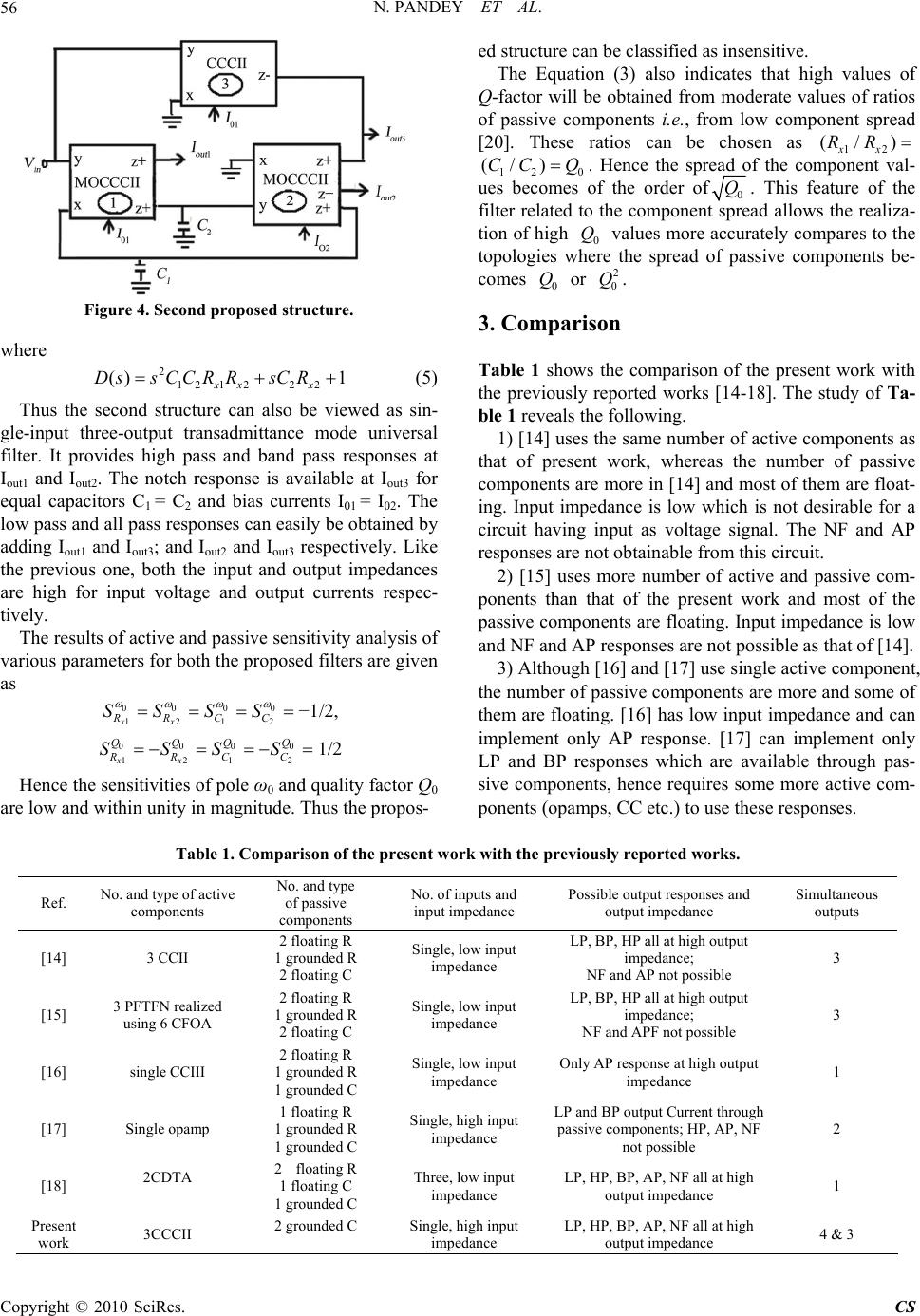 N. PANDEY ET AL. Copyright © 2010 SciRes. CS 56 Figure 4. Second proposed structure. where 2 12 1 222 () 1 xx x DssCCRRsCR (5) Thus the second structure can also be viewed as sin- gle-input three-output transadmittance mode universal filter. It provides high pass and band pass responses at Iout1 and Iout2. The notch response is available at Iout3 for equal capacitors C1 = C2 and bias currents I01 = I02. The low pass and all pass responses can easily be obtained by adding Iout1 and Iout3; and Iout2 and Iout3 respectively. Like the previous one, both the input and output impedances are high for input voltage and output currents respec- tively. The results of active and passive sensitivity analysis of various parameters for both the proposed filters are given as 00 00 1212xx RRCC SSSS −1/2, 0000 1212xx QQQQ RRCC SSSS 1/2 Hence the sensitivities of pole ω0 and quality factor Q0 are low and within unity in magnitude. Thus the propos- ed structure can be classified as insensitive. The Equation (3) also indicates that high values of Q-factor will be obtained from moderate values of ratios of passive components i.e., from low component spread [20]. These ratios can be chosen as 12 (/ ) xx RR 12 0 (/ )CC Q . Hence the spread of the component val- ues becomes of the order of0 Q. This feature of the filter related to the component spread allows the realiza- tion of high 0 Q values more accurately compares to the topologies where the spread of passive components be- comes 0 Q or 2 0 Q. 3. Comparison Table 1 shows the comparison of the present work with the previously reported works [14-18]. The study of Ta- ble 1 reveals the following. 1) [14] uses the same number of active components as that of present work, whereas the number of passive components are more in [14] and most of them are float- ing. Input impedance is low which is not desirable for a circuit having input as voltage signal. The NF and AP responses are not obtainable from this circuit. 2) [15] uses more number of active and passive com- ponents than that of the present work and most of the passive components are floating. Input impedance is low and NF and AP responses are not possible as that of [14]. 3) Although [16] and [17] use single active component, the number of passive components are more and some of them are floating. [16] has low input impedance and can implement only AP response. [17] can implement only LP and BP responses which are available through pas- sive components, hence requires some more active com- ponents (opamps, CC etc.) to use these responses. Table 1. Comparison of the present work with the previously reported works. Ref. No. and type of active components No. and type of passive components No. of inputs and input impedance Possible output responses and output impedance Simultaneous outputs [14] 3 CCII 2 floating R 1 grounded R 2 floating C Single, low input impedance LP, BP, HP all at high output impedance; NF and AP not possible 3 [15] 3 PFTFN realized using 6 CFOA 2 floating R 1 grounded R 2 floating C Single, low input impedance LP, BP, HP all at high output impedance; NF and APF not possible 3 [16] single CCIII 2 floating R 1 grounded R 1 grounded C Single, low input impedance Only AP response at high output impedance 1 [17] Single opamp 1 floating R 1 grounded R 1 grounded C Single, high input impedance LP and BP output Current through passive components; HP, AP, NF not possible 2 [18] 2CDTA 2 floating R 1 floating C 1 grounded C Three, low input impedance LP, HP, BP, AP, NF all at high output impedance 1 Present work 3CCCII 2 grounded C Single, high input impedance LP, HP, BP, AP, NF all at high output impedance 4 & 3 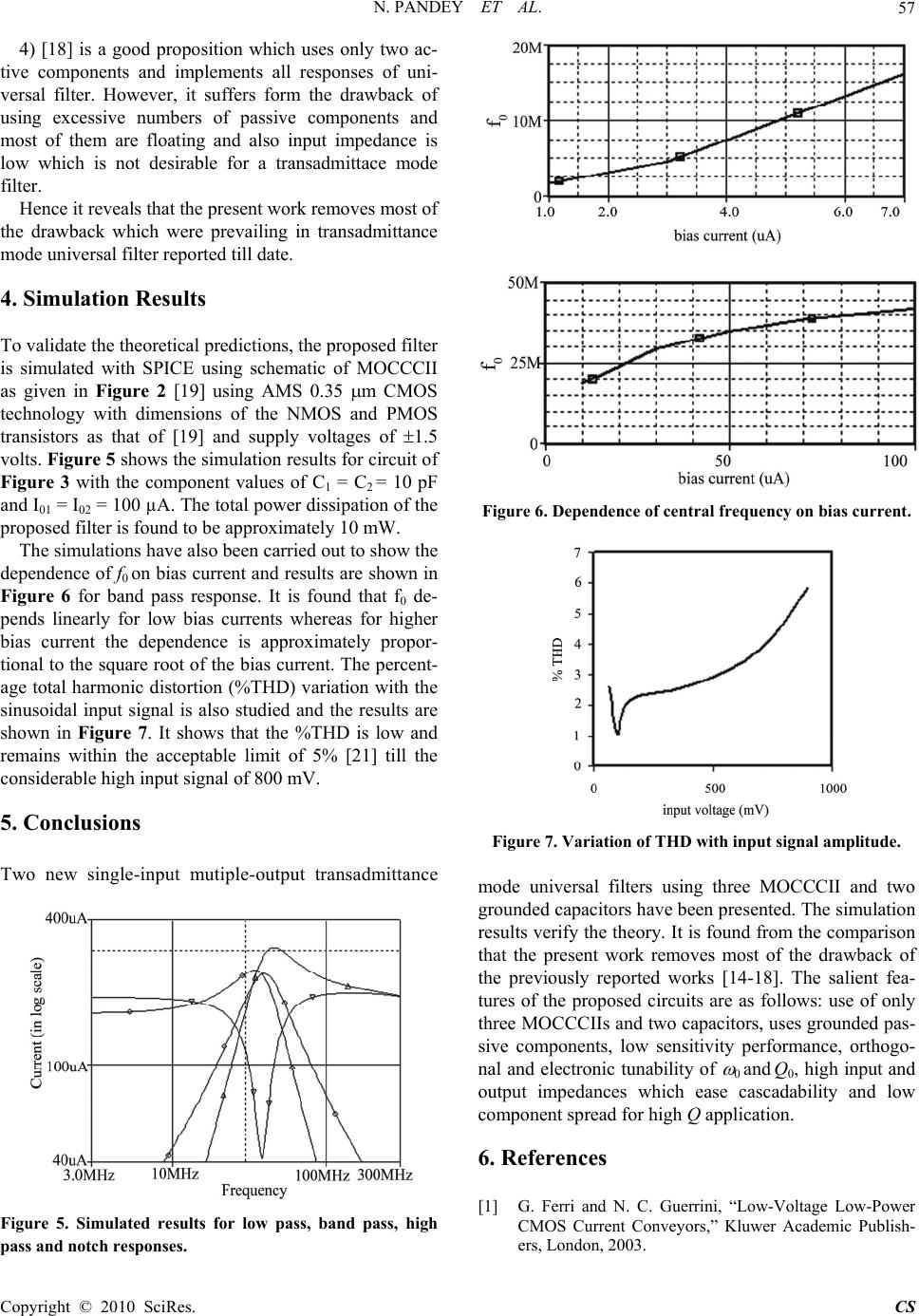 N. PANDEY ET AL. Copyright © 2010 SciRes. CS 57 4) [18] is a good proposition which uses only two ac- tive components and implements all responses of uni- versal filter. However, it suffers form the drawback of using excessive numbers of passive components and most of them are floating and also input impedance is low which is not desirable for a transadmittace mode filter. Hence it reveals that the present work removes most of the drawback which were prevailing in transadmittance mode universal filter reported till date. 4. Simulation Results To validate the theoretical predictions, the proposed filter is simulated with SPICE using schematic of MOCCCII as given in Figure 2 [19] using AMS 0.35 m CMOS technology with dimensions of the NMOS and PMOS transistors as that of [19] and supply voltages of 1.5 volts. Figure 5 shows the simulation results for circuit of Figure 3 with the component values of C1 = C2 = 10 pF and I01 = I02 = 100 µA. The total power dissipation of the proposed filter is found to be approximately 10 mW. The simulations have also been carried out to show the dependence of f0 on bias current and results are shown in Figure 6 for band pass response. It is found that f0 de- pends linearly for low bias currents whereas for higher bias current the dependence is approximately propor- tional to the square root of the bias current. The percent- age total harmonic distortion (%THD) variation with the sinusoidal input signal is also studied and the results are shown in Figure 7. It shows that the %THD is low and remains within the acceptable limit of 5% [21] till the considerable high input signal of 800 mV. 5. Conclusions Two new single-input mutiple-output transadmittance Figure 5. Simulated results for low pass, band pass, high pass and notch responses. Figure 6. Dependence of central frequency on bias current. Figure 7. Variation of THD with input signal amplitude. mode universal filters using three MOCCCII and two grounded capacitors have been presented. The simulation results verify the theory. It is found from the comparison that the present work removes most of the drawback of the previously reported works [14-18]. The salient fea- tures of the proposed circuits are as follows: use of only three MOCCCIIs and two capacitors, uses grounded pas- sive components, low sensitivity performance, orthogo- nal and electronic tunability of 0 and Q0, high input and output impedances which ease cascadability and low component spread for high Q application. 6. References [1] G. Ferri and N. C. Guerrini, “Low-Voltage Low-Power CMOS Current Conveyors,” Kluwer Academic Publish- ers, London, 2003.  N. PANDEY ET AL. Copyright © 2010 SciRes. CS 58 [2] N. A. Shah, M. F. Rather and S. Z. Iqbal, “Multifunction Mixed Mode Filter Using FTFN,” Analog Integrated Cir- cuits and Signal Processing, Vol. 47, No. 3, 2006, pp. 339-343. [3] A. Fabre, O. Saaid, F. Wiest and C. Boucheron, “High Frequency Applications Based on a New Current Con- trolled Conveyor,” IEEE Transactions on Circuits Sys- tems-I, Vol. 43, No. 2, 1996, pp. 82-91. [4] N. Pandey, S. K. Paul and S. B. Jain, “A New Electroni- cally Tunable Current Mode Universal Filter Using MO- CCCII,” Analog Integrated Circuits and Signal Process- ing, Vol. 58, No. 2, 2009, pp. 171-178. [5] S. Ozoguz, A. Toker and O. Cicekoglu, “New Current- Mode Universal Filters Using Only CCII + s,” Microe- lectronics Journal, Vol. 30, No. 3, 1999, pp. 255-258. [6] W. Tangsrirat, “Current Tunable Current Mode Multi- function Filter Based on Dual Output Current Controlled Conveyors,” AEU International Journal of Electronics and Communications, Vol. 61, No. 8, 2007, pp. 528-533. [7] J. W. Horng, C. L. Hou, C. M. Chang and W. Y. Chung, “Voltage Mode Universal Biquadratic Filters with One Input and Five Outputs,” Analog Integrated Circuits and Signal Processing, Vol. 47, No. 1, 2006, pp. 73-83. [8] O. Cicekoglu and H. Kuntman, “A New Four Terminal Floating Nullor Base Single-Input Three-Output Current- Mode Multifunction Filter,” Microelectronics Journal, Vol. 30, No. 2, 1999, pp. 115-118. [9] D. R. Bhaskar, V. K. Sharma, M. Monis and S. M. I. Rizvi, “New Current Mode Universal Biquad Filter,” Microelec- tronics Journal, Vol. 30, No. 9, 1999, pp. 837-839. [10] A. Fabre and M. Alami, “Universal Current Mode Biquad Implemented from Two Second Generation Current Con- veyors,” IEEE Transactions on Circuits Systems-I, Vol. 42, No. 7, 1995, pp. 383-385. [11] A. Fabre, F. Dayoub, L. Duruisseau and M. Kamoun, “High Input Impedance Insensitive Second-Order Filters Implemented from Current Conveyors,” IEEE Transac- tions on Circuits Systems-I, Vol. 41, No. 12, 1994, pp. 918-921. [12] I. A. Khan and M. H. Zaidi, “Multifunction Translinear-C Current Mode Filter,” International Journal of Electron- ics, Vol. 87, No. 6, 2000, pp. 1047-1051. [13] S. Maheshwari and I. A. Khan, “Novel Cascadable Cur- rent-Mode Translinear-C Universal Filter,” Active and Passive Electronic Components, Vol. 27, No. 4, 2004, pp. 215-218. [14] A. Toker, O. Cicekoglu, S. Ozacan and H. Kuntman, “High Output Impedance Transadmittance Type Con- tinuous Time Multifunction Filter with Minimum Active Elements,” International Journal of Electronics, Vol. 88, No. 10, 2001, pp. 1085-1091. [15] N. A. Shah, S. Z. Iqbal and B. Parveen, “SITO High Output Impedance Transadmittance Filter Using FTFNs,” Analog Integrated Circuits and Signal Processing, Vol. 40, No. 4, 2004, pp. 87-89. [16] U. Cam, “A New Transadmittance Type First-Order All Pass Filter Employing Single Third Generation Current Conveyor,” Analog Integrated Circuits and Signal Proc- essing, Vol. 43, No. 1, 2005, pp. 97-99. [17] N. A. Shah, S. Z. Iqbal and B. Parveen, “Lowpass and Bandpass Transadmittance Filter Using Operational Am- plifier Pole,” AEU International Journal of Electronics and Communications, Vol. 59, No. 7, 2005, pp. 410-412. [18] N. A. Shah, M. Quadri and S. Z. Iqbal, “CDTA Based Universal Transadmittance Filter,” Analog Integrated Circuits and Signal Processing, Vol. 52, No. 1-2, 2007, pp. 65-69. [19] E. Altuntas and A. Toker, “Realization of Voltage and Current Mode KHN Biquad Using CCCIIs,” AEU Inter- national Journal of Electronics and Communications, Vol. 56, No. 1, 2002, pp. 45-49. [20] S. I. Liu, “High Input Impedance Filter with Low Com- ponent Spread Using Current Feedback Amplifiers,” Electronics Letters, Vol. 31, No. 13, 1995, pp. 1042- 1043. [21] E. S. Erdogan, R. O. Topaloglu, H. Kuntman and O. Cicekoglu, “New Current Mode Special Function Con- tinuous-Time Active Filters Employing only OTAs and OPAMPs,” International Journal of Electronics, Vol. 91, No. 6, 2004, pp. 345-359. |