Paper Menu >>
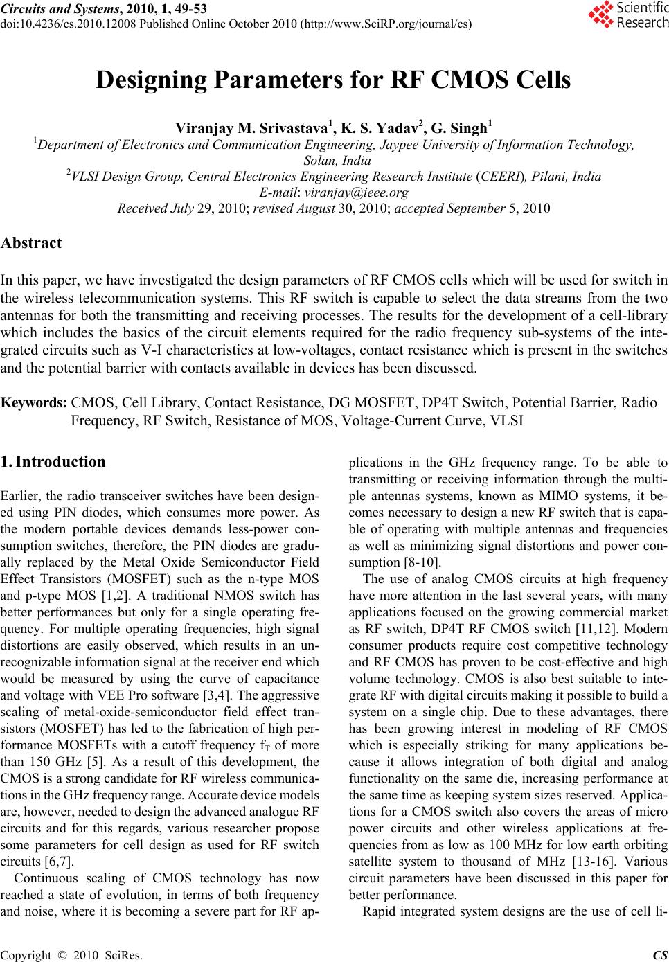
Journal Menu >>
 Circuits and Systems, 2010, 1, 49-53 doi:10.4236/cs.2010.12008 Published Online October 2010 (http://www.SciRP.org/journal/cs) Copyright © 2010 SciRes. CS Designing Parameters for RF CMOS Cells Viranjay M. Srivastava1, K. S. Yadav2, G. Singh1 1Department of Electronics and Communication Engineering, Jaypee University of Information Technology, Solan, India 2VLSI Design Group, Central Electronics Engineering Research Institute (CEERI), Pilani, India E-mail: viranjay@ieee.org Received July 29, 2010; revised August 30, 2010; accepted September 5, 2010 Abstract In this paper, we have investigated the design parameters of RF CMOS cells which will be used for switch in the wireless telecommunication systems. This RF switch is capable to select the data streams from the two antennas for both the transmitting and receiving processes. The results for the development of a cell-library which includes the basics of the circuit elements required for the radio frequency sub-systems of the inte- grated circuits such as V-I characteristics at low-voltages, contact resistance which is present in the switches and the potential barrier with contacts available in devices has been discussed. Keywords: CMOS, Cell Library, Contact Resistance, DG MOSFET, DP4T Switch, Potential Barrier, Radio Frequency, RF Switch, Resistance of MOS, Voltage-Current Curve, VLSI 1. Introduction Earlier, the radio transceiver switches have been design- ed using PIN diodes, which consumes more power. As the modern portable devices demands less-power con- sumption switches, therefore, the PIN diodes are gradu- ally replaced by the Metal Oxide Semiconductor Field Effect Transistors (MOSFET) such as the n-type MOS and p-type MOS [1,2]. A traditional NMOS switch has better performances but only for a single operating fre- quency. For multiple operating frequencies, high signal distortions are easily observed, which results in an un- recognizable information signal at the receiver end which would be measured by using the curve of capacitance and voltage with VEE Pro software [3,4]. The aggressive scaling of metal-oxide-semiconductor field effect tran- sistors (MOSFET) has led to the fabrication of high per- formance MOSFETs with a cutoff frequency fT of more than 150 GHz [5]. As a result of this development, the CMOS is a strong candidate for RF wireless communica- tions in the GHz frequency range. Accurate device models are, however, needed to design the advanced analogue RF circuits and for this regards, various researcher propose some parameters for cell design as used for RF switch circuits [6,7]. Continuous scaling of CMOS technology has now reached a state of evolution, in terms of both frequency and noise, where it is becoming a severe part for RF ap- plications in the GHz frequency range. To be able to transmitting or receiving information through the multi- ple antennas systems, known as MIMO systems, it be- comes necessary to design a new RF switch that is capa- ble of operating with multiple antennas and frequencies as well as minimizing signal distortions and power con- sumption [8-10]. The use of analog CMOS circuits at high frequency have more attention in the last several years, with many applications focused on the growing commercial market as RF switch, DP4T RF CMOS switch [11,12]. Modern consumer products require cost competitive technology and RF CMOS has proven to be cost-effective and high volume technology. CMOS is also best suitable to inte- grate RF with digital circuits making it possible to build a system on a single chip. Due to these advantages, there has been growing interest in modeling of RF CMOS which is especially striking for many applications be- cause it allows integration of both digital and analog functionality on the same die, increasing performance at the same time as keeping system sizes reserved. Applica- tions for a CMOS switch also covers the areas of micro power circuits and other wireless applications at fre- quencies from as low as 100 MHz for low earth orbiting satellite system to thousand of MHz [13-16]. Various circuit parameters have been discussed in this paper for better performance. Rapid integrated system designs are the use of cell li- 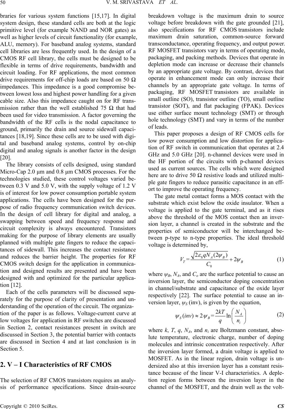 V. M. SRIVASTAVA ET AL. Copyright © 2010 SciRes. CS 50 braries for various system functions [15,17]. In digital system design, these standard cells are both at the logic primitive level (for example NAND and NOR gates) as well as higher levels of circuit functionality (for example, ALU, memory). For baseband analog systems, standard cell libraries are less frequently used. In the design of a CMOS RF cell library, the cells must be designed to be flexible in terms of drive requirements, bandwidth and circuit loading. For RF applications, the most common drive requirements for off-chip loads are based on 50 Ω impedances. This impedance is a good compromise be- tween lowest loss and highest power handling for a given cable size. Also this impedance caught on for RF trans- mission rather than the well established 75 Ω that had been used for video transmission. A factor governing the bandwidth of the RF cells is the nodal capacitance to ground, primarily the drain and source sidewall capaci- tances [18,19]. Since these cells are to be used with digi- tal and baseband analog systems, control by on-chip digital and analog signals is another factor in the design [20]. The library consists of cells designed, using standard Micro-Cap 2.0 μm and 0.8 μm CMOS processes. For the technologies studied, these control voltages varied be- tween 0.3 V and 5.0 V, with the supply voltage of 1.2 V is of interest for low power consumption portable system applications. The cells have been designed for the pur- pose of radio frequency communication switch devices. In the design of cell library for digital and analog, a swapping between speed and frequency response and circuit complexity is always encountered. Transistors making for the purpose of library elements are usually planned with multiple gate fingers to reduce the capaci- tances of sidewall. This increases the contact resistance and reduces the barrier height. The properties for RF CMOS switch design for the application in communica- tion and designed results are presented and have been designed with and optimized for the particular applica- tion [12]. Each of the cells parameters will be discussed sepa- rately for the purpose of clarity of presentation and un- derstanding of the operation of the circuit. The organiza- tion of the paper is as follows. Voltage-current curve at low voltages for application in RF switches are discussed in Section 2, contact resistances present in switch are discussed in Section 3, the potential barrier with contacts are discussed in Section 4 and at last conclusion is in Section 5. 2. V – I Characteristics of RF CMOS The selection of RF CMOS transistors requires an analy- sis of performance specifications. Since drain-source breakdown voltage is the maximum drain to source voltage before breakdown with the gate grounded [21], also specifications for RF CMOS transistors include maximum drain saturation, common-source forward transconductance, operating frequency, and output power. RF MOSFET transistors vary in terms of operating mode, packaging, and packing methods. Devices that operate in depletion mode can increase or decrease their channels by an appropriate gate voltage. By contrast, devices that operate in enhancement mode can only increase their channels by an appropriate gate voltage. In terms of packaging, RF MOSFET transistors are available in small outline (SO), transistor outline (TO), small outline transistor (SOT), and flat packaging (FPAK). Devices use either surface mount technology (SMT) or through hole technology (SMT) and vary in terms of the number of leads. This paper proposes a design of RF CMOS cells for low power consumption and low distortion for applica- tion of RF switch in communication that operates at 2.4 GHz and 5.0 GHz [20]. n-channel devices were used in the HF portion of the circuits with p-channel devices used as current sources. The cells which were designed here are to drive 50 Ω resistive loads and utilized multi- ple gate fingers to reduce parasitic capacitance in an eff- ort to improve the operating frequency. The gate metal contact forms a MOS contact with the substrate which exist below the oxide insulator. When a voltage is applied to the gate terminal, and as it rises above the threshold of the MOS contact then an inver- sion layer, a channel is created in the substrate and the properties of semiconductor will be interchanged be- tween p-type to n-type properties. The ideal threshold voltage is determined by, S 0 2(2) =2 AB TB qN VC (1) where ψB, NA, and Co are the surface potential to cause an inversion layer, the semiconductor doping concentration in channel/substrate and capacitance of the oxide layer respectively [22]. The surface potential to cause an in- version layer, ψS (inv), is given by the equation, 2 ()2=ln A SB i N kT inv qn (2) where k, T, q, NA, and ni are Boltzmann constant, abso- lute temperature, electronic charge, number of doping molecules and intrinsic concentration respectively. After the inversion layer formed, a drain voltage is applied to MOSFET. As in the linear region, drain voltage is un- dersized also at this inversion layer has a constant resis- tance because of the linear V-I characteristics. A deple- tion region forms between the inversion layer in the channel of the MOSFET, and the drain well as the volt-  V. M. SRIVASTAVA ET AL. Copyright © 2010 SciRes. CS 51 age difference from the drain to gate increases to more than VT. This causes the current to reach a maximum current (saturation current, IDsat,). For the fabricated device with gate oxide thickness (tox) 650 Å, oxide capacitance (Cox) 5.31*10-8 F/cm2 [23], channel length (L) 0.8 µm, channel width (W) 400 µm, mobility 800 cm2/V-s, channel doping (NB) 1015/cm3 so we found the Vth 0.867 V and found the drain current as shown in Figure 1 with different drain voltage range. Similarly, with the gate voltage range (VG) 0.3 V to 2.1 V, step size 0.3 V drain voltage range (VD) 0 V to 1.5 V, we found the drain current 3.8 mA for VG 1.5 V, 8.0 mA for VG 1.8 V, and 13.6 mA for VG 2.1 V. A RF CMOS has the properties as fixed tuned match- ing networks, low Q matching networks, ruggedness, high power output, mounting flange packages, and Sili- con grease. Power gain (a measure of power amplifica- tion, is the ratio of output power to input power, dB), Noise figure (a measure of the amount of noise added during normal operation, is the ratio of the signal-to- noise ratio at the input and the signal-to-noise ratio at the output, dB), High power dissipation (a measure of total power consumption, W or mW). Some bipolar RF CMOS transistors are suitable for automotive, commer- cial or general industrial applications. 3. Contact Resistances For measuring the contact resistance of a metal-semicon- ductor junction of MOSFET, deposition of metal on the semiconductor are required and it patterns, so that vari- ous identical pads spaced with different distances as shown in Figure 2. These patterns include many rows of different pad sizes. The pads in any one row should be of same size, whereas the distances between pads are varying. The measurements required simple voltage and current curves. Figure 1. Gate voltage range (VG) = 0.3 V to 1.2 V, step size = 0.1 V, drain voltage range (VD) = 0 to 0.5 V. For calculating the resistance, we apply a voltage be- tween some pairs of adjoining pads in of a row, and measure the current flow. From this, calculate the resis- tance between those two pads. As shown in Figure 2, the total resistance between any two pads is the series com- bination of following three resistors; metal to semicon- ductor, through the semiconductor and back into metal. Since ohmic contacts are the same for both polarities, so R = 2Rpad + Rsemi as shown in Figure 3. When the distance between two pads tends to zero, then resistance through the semiconductor (Rsemi) goes to zero and only resistance between metal to semiconductor and back into metal will be left (2Rpad). Now we have Rpad, multiply that value by the area of the metal pads (in cm2). For author’s circuit it is taken as 10-5 Ω-cm2. Con- sider that in the modern processes, the vias that contact the silicon have a contact area of about 0.1 μm2 or 10-8 cm2. If contact resistance is 10-5 Ωcm2, that amounts to 1.0 kΩ resistor to get into the silicon (plus another to get out). A good contact resistance is on the order of 10-7 Ωcm2. The Schottky contact resistance between the silicide layer and polysilicon is the most likely cause of the ex- cessive gate resistance and as measured using above techniques. The contact resistance values, which are in good agreement with the result as shown in Figure 3, for monolithic silicon, were shown to contribute substantially to the gate resistance. Downscaling of CMOS technolo- gies will make the problem more pronounced, since the interface contact resistance is inversely proportional to the total gate area as in term of length and width of a gate. The reduction of resistance should lead to improved RF Figure 2. Example of the metal pattern of a RF MOSFET. 05 10 15 20 25 3035 40 45 5 0 20 30 40 50 60 70 Length between pads(um) Calculated Resistance(ohm) Figure 3. Resistance variation with pad lengths.  V. M. SRIVASTAVA ET AL. Copyright © 2010 SciRes. CS 52 properties in MOSFETs [6,24,25]. 4. Potential Barriers Potential barrier exist between metal and semiconductor layer when they are in close contact, this stops the ma- jority of charge carriers to pass from one layer to the other layer. Only a few charge carriers have an adequate amount of energy to pass though the barrier and cross to the other side material. After applying a bias voltage to the junction, it has following two effects, first it can cre- ate the barrier come into view lower from the semicon- ductor side, or second, it can make so higher. But the bias does not change the barrier height from the metal side. This creates a Schottky Barrier also known as rec- tifying contact, where junction conducts only for one bias polarity, not the other. This rectifying contact makes good diodes and can even be used to make a kind of transistor. A direct method of potential barrier height determina- tion is presented in this section. The best agreement between the barrier heights determined this method using a dependence of the Si-SiO2 interface barrier height on the thickness of the aluminium gate has been observed [15]. Since the barrier height is the property of a material, so we try to use these materials for the CMOS in appli- cation of RF, whose barrier height is small. Here is a possibility to create an alloy between metal and semi- conductor junction, at the time of annealing, which low- ers the barrier height [26]. The probability of tunneling becomes high for extremely thin barriers (in the tens of nanometers). By the heavy doping process one can make the very thin barrier which is approximately doing con- centration of 1019 dopant atoms/cm3 or more. As the barrier height is closer to zero, ohmic contact increases. For this one can concludes the following result as shown in Table 1, for a positive barrier height. Aluminium (Al), for doping of polysilicon 1015/cm3, n-type, p-Silicon, semiconductor barrier height will 0.92 eV and metal-semiconductor junction depletion layer width is 0.284 μm wide. Ploysilicon, doping of polysilicon 1015/cm3, n-type, p- Silicon, semiconductor barrier height will 0.85 eV and metal-semiconductor junction depletion layer width is 0 wide. So for the polysilicon, we achieve the barrier height is closer to zero, which increases the ohmic contact. Table 1. Direction of current flow. Type Current flow into (easily) n semiconductor p metal 5. Results and Conclusions After calculation of the currents, resistance and potential barrier, we conclude that the drain current increases with increase of the gate voltage or control voltage. Also, the MOS device parameters can be used with VEE Pro- gramming [27]. For the purpose of RF switch, where control voltage should be low and then current flow will be less and in terms of contact resistance, it will in- creases with increase in number of gate fingers. So in application of RF switch authors have tried to lower the gate finger. The semiconductor barrier height and deple- tion layer width is more for aluminum compare to polysilicon metal-semiconductor junction which is 0.284 μm wide. Since the operating frequencies of the RF switches are in the order of GHz, therefore, it is useful for wireless local area network (WLAN) and other IEEE 802.11 applications. 6. Acknowledgements The authors would like to thank Prof. A. B. Bhattach- haraya, Jaypee Institute of Information Technology, In- dia and Mr. Peeyush Tripathi, Intel Corporation, Banga- lore, India for insightful discussions. 7. References [1] Skyworks Solutions Inc., “Application Note, APN1002, Design with PIN Diodes,” Woburn, July 2005. [2] J. Park and Z. Q. Ma, “A 15 GHz CMOS RF Switch Em- ploying Large Signal Impedance Matching,” Proceeding of Topical Meeting on Silicon Monolithic Integrated Cir- cuits in RF Systems, Denver, 2006, pp. 1-4. [3] M. Viranjay Srivastava, K. S. Yadav and G. Singh, “Ap- plication of VEE Pro Software for Measurement of MOS Device Parameter Using C-V Curve,” International Journal of Computer Applications, Vol. 1, No. 7, March 2010, pp. 43-46. [4] V. M. Srivastava, “Capacitance-Voltage Measurement for Characterization of a Metal Gate MOS Process,” Inter- national Journal of Recent Trends in Engineering, Vol. 1, No. 4, May 2009, pp. 4-7. [5] A. Litwin, E. Microelectron and A. B. Stockholm, “Overlooked Interfacial Silicide-Polysilicon Gate Resis- tance in MOS Transistors,” IEEE Transactions on Elec- tron Devices, Vol. 48, No. 9, September 2001, pp. 2179- 2181. [6] V. M. Srivastava, K. S. Yadav and G. Singh, “Attenuation with Double Pole Four Throw CMOS Switch Design,” IEEE International Conference on Semiconductor Elec- tronics (ICSE-2010), Malacca, 28-30 June 2010, pp. 173- 175. [7] Y. J. Chan, C. H. Huang, C. C. Weng and B. K. Liew,  V. M. SRIVASTAVA ET AL. Copyright © 2010 SciRes. CS 53 “Characteristics of Deep Sub-Micrometer MOSFET and its Empirical Non-Linear RF Model,” IEEE Transaction on Microwave Theory, Vol. 46, No. 5, May 1998, pp. 611- 615. [8] J. P. Carmo, P. M. Mendes, C. Couto and J. H. Correia “A 2.4-GHz RF CMOS Transceiver for Wireless Sensor Applications,” Proceeding of International Conference on Electrical Engineering, Coimbra, 2005, pp. 902-905. [9] P. Mekanand and D. Eungdamorang, “DP4T CMOS Switch in a Transceiver of MIMO System,” Proceeding of 11th IEEE International Conference of Advanced Communication Technology, Korea, 2009, pp. 472-474. [10] P. H. Woerlee, M. J. Knitel, R. V. Langevelde, D. B. Klaassen, L. F. Tiemeijer and A. J. Scholten, “RF CMOS Performance Trends,” IEEE Transaction on Electron De- vices, Vol. 48, No. 8, August 2001, pp. 1776-1782. [11] T. H. Lee, “CMOS RF No Longer an Oxymoron,” Pro- ceedings of the 19th Gallium Arsenide Integrated Circuit Symposium, Anaheim, 1997, pp. 244-247. [12] V. M. Srivastava, K. S. Yadav and G. Singh, “Double Pole Four Throw Switch Design with CMOS Inverter,” Proceeding of 5th IEEE International Conference on Wireless Communication and Sensor Network, Kolkata, 15-19 December 2009, pp. 1-4. [13] S. Lee, C. Yoo, W. Kim, H. K. Ryu and W. Song, “1 GHz CMOS Down Conversion Mixer,” Proceeding of IEEE International Symposium on Consumer Electronics, Singapore, 1997, pp. 125-127. [14] T. H. Lin, H. Sanchez, R. Rofougaran and W. J. Kaiser, “CMOS Front End Components for Micropower RF Wireless Systems,” Proceeding of International Sym- posium on Low Power Electronics and Design, Monterey, California, 1998, pp. 11-15. [15] F. Piazza, P. Orsatti, Q. Huang and T. Morimoto, “0.25 mm CMOS Transceiver Front-End for GSM,” Procee- ding of IEEE Custom Integrated Circuits Conference, Singapore, 1998, pp. 413-416. [16] T. Manku, “Microwave CMOS Device Physics and De- sign,” IEEE Journal of Solid State Circuits, Vol. 34, No. 3, March 1999, pp. 277-285. [17] C. Laber, C. Rahim, S. Dreyer, G. Uehara, P. Kwok and P. Gray, “Design Considerations for a High Performance 3 Micron CMOS Analog Standard Cell Library,” IEEE Journal of Solid State Circuits, Vol. 22, No. 2, 1987, pp. 181-189. [18] Y. Cheng, and M. Matloubian, “Frequency Dependent Resistive and Capacitive Components in RF MOSFETs,” IEEE Electron Device Letters, Vol. 22, No. 7, July 2001, pp. 333-335. [19] K. J. Yang and C. Hu, “MOS Capacitance Measurements for High Leakage Thin Dielectrics,” IEEE Transaction on Electron Devices, Vol. 46, No. 7, July 1997, pp. 1500- 1501. [20] M. Smith, C. Portman, C. Anagnostopoulos, P. Tschang, R. Rao, P. Valdenaire and H. Ching, “Cell Libraries and Assembly Tools for Analog/Digital CMOS and BiCMOS ASIC Design,” IEEE Journal of Solid State Circuits, Vol. 24, No. 5, 1989, pp. 1419-1432. [21] S. H. Lee, C. S. Kim and H. K. Yu, “A Small Signal RF Model and its Parameter Extraction for Substrate Effects in RF MOSFETs,” IEEE Transaction on Electron Devices, Vol. 48, No. 7, July 2001, pp. 1374-1379. [22] N. Talwalkar, C. Patrick Yue and S. Simon Wong, “In- tegrated CMOS Transmit-Receive Switch Using LC- Tuned Substrate Bias for 2.4 GHz and 5.2 GHz Appli- cations,” IEEE Journal of Solid State Circuits, Vol. 39, No. 6, 1989, pp. 863-870. [23] V. M. Srivastava, K. S. Yadav and G. Singh, “Measure- ment of Oxide Thickness for MOS Devices, Using Simu- lation of SUPREM Simulator,” International Journal of Computer Applications, Vol. 1, No. 6, March 2010, pp. 66-70. [24] Y. Cheng and M. Matloubian, “Parameter Extraction of Accurate and Scaleable Substrate Resistace Components in RF MOSFETs,” IEEE Electron Device Letters, Vol. 23, No. 4, April 2002, pp. 221-223. [25] Y. S. Lin, S. S. Lu, T. S. Lee and H. B. Liang, “Charac- terization and Modeling of Small Signal Substrate Resis- tance Effect in RF CMOS,” IEEE MTT-S Digest, June 2002, pp. 161-164. [26] S. M. Sze, “Semiconductor Devices: Physics and Tech- nology,” 2nd Edition, Tata McGraw Hill, Noida, 2004. [27] V. M. Srivastava, “Relevance of VEE Programming for Measurement of MOS Device Parameters,” Proceedings of IEEE International Advance Computing Conference, Patiala, March 2009, pp. 205-209. |