Circuits and Systems, 2013, 4, 67-74
http://dx.doi.org/10.4236/cs.2013.41011 Published Online January 2013 (http://www.scirp.org/journal/cs)
Behavioral Modeling and Simulation of Cascade Multibit
ΣΔ Modulator for Multistandard Radio Receiver
Sonia Zouari1, Houda Daoud1, Mourad Loulou1, Patrick Loumeau2, Nouri Masmoudi1
1Information Technologies and Electronics Laboratory National Engineering School of Sfax, Sfax, Tunisia
2Electronics and Communications Department, Telecom ParisTech, Paris, France
Email: sonia.zouari@enis.rnu.tn, daoud.houda@tunet.tn, mourad.loulou@ieee.org, Patrick.loumeau@enst.fr
Received July 25, 2012; revised September 19, 2012; accepted September 27, 2012
ABSTRACT
In this paper, a cascade Sigma-Delta (ΣΔ) Analog to Digital Converter (ADC) for multistandard radio receiver was pre-
sented. This converter is supposed to be able to support GSM, UMTS, Wifi and WiMAX communication standards.
The Sigma-Delta modulator makes use of 4 bit quantizer and Data-Weighted-Averaging (DWA) technique to attain
high linearity over a wide bandwidth. A top-down design methodology was adopted to provide a reliable tool for the
design of reconfigurable high-speed ΣΔMs. VHDL-AMS language was used to model the analog and mixed parts of the
selected 2-1-1 cascade ΣΔ converter and to verify their reconfiguration parameters based on behavioural simulation.
This multistandard architecture was high level sized to adapt the modulator performance to the different standards re-
quirements. The effects of circuit non-idealities on the modulator performance were modeled and analyzed in VHDL-
AMS to extract the required circuit parameters.
Keywords: ΔΣ ADC; Multistandard; VHDL-AMS Language; Behavioural Simulation
1. Introduction
The most significant design challenge in current and fu-
ture wireless devices is to support several wireless and
cellular standards in the same handheld device. The goal
was to design multistandard RF terminals that are very
flexible and reconfigurable with neither a decrease in the
circuit performance nor an increase in power consump-
tion or silicon area [1-4]. A high resolution high speed
ADC will only allow the shifting of several RF and ana-
log processing to the digital domain in order to provide
more flexibility and increase the design complexity [5].
The use of ΔΣ modulators in multistandard receivers is
suitable for several reasons among which we can cite,
firstly, that ΣΔ modulators are very linear and are also
less sensitive to circuit non-idealities than other types of
data converters [6]. Secondly, the noise shaping and the
oversampling performed by ΣΔ modulators allow to
achieve high Dynamic Range (DR) for narrow band-
widths and lower DR for higher bandwidths. This char-
acteristic is coherent with wireless standards require-
ments and their RF specifications which makes ΣΔ ADC
suitable to perform the Analog/Digital (A/D) conversion
function in a multi-standard capable RF receiver [7]. An-
other important advantage of ΣΔ ADC is it consumes less
power than full Nyquist ADCs [8]. In this paper, the re-
configurable ΣΔ was modelled to be designed for a
GSM/UMTS/WiFi/WiMAX radio receiver. Figure 1
shows the adopted multistandard receiver architecture.
The proposed architecture is a multistandard Zéro-IF
receiver. It uses a multiband antenna, four RF filters for
GSM/UMTS/WLAN/WiMAX selection, a multistandard
low noise amplifier (LNA) and multistandard mixers for
I and Q components. The A/D conversion is performed
with multistandard anti Alias filter and multistandard ΣΔ
Modulator (ΣΔ M). The digital processing is supported
by a DSP circuit. Zero_IF architecture was chosen for its
high level of integration, associated with excellent multi-
standard capabilities [9]. Contrary to several multistan-
dard Zero-IF architectures proposed in literature which
use channel selection in analog domain and use an auto-
matic Gain Control (AGC) to decrease ADC dynamic
requirement [10,11], in our selected multistandard re-
ceiver, channel selection is performed in the digital do-
main and a very high dynamic ADC is used to eliminate
the need for AGC. It uses a multistandard oversampled
ΔΣ M followed by a digital decimation filter as shown in
Figure 2. This approach achieves a more programmable
solution rather than an analog approach thereby, enabling
such receivers to upgrade easy to multi-mode operation.
Digital channel select filtering can be made easily pro-
grammable by changing the filter coefficients in the deci-
mation filter. However, the dynamic range of the ADC
must also be made programmable to fit the RF specifica-
C
opyright © 2013 SciRes. CS
S. ZOUARI ET AL.
68
tions. Fortunately, Sigma-Delta modulators allow the de-
signer to trade off bandwidth and dynamic range which
make them suitable to perform the A/D conversion func-
tion in a multi-standard capable RF receiver. Relying on
system specifications for various addressed RF commu-
nications standards and on chosen receiver characteristics,
ADC specifications were established for each standard
(Table 1).
The remaining of the paper is organized as follows:
Section 2 shows the multistandard cascaded Sigma-Delta
modulator architecture and discusses its reconfiguration.
Section 3 describes the system level design of the pro-
posed modulator using VHDL-AMS language. The simu-
lation results modeling are presented in Section 4. Finally,
we draw our conclusion in Section 5.
2. Reconfigurable ΣΔ Modulator
Architecture
Given that reconfigurability must be considered to find
out the optimal multistandard ΣΔ modulator architecture,
the cascade ΣΔ ADC was selected as the best suited ar-
chitecture (Figure 3) [12-14]. This fourth order cascade
GSM RF Filter
Antenne
multibande
UMTS RF Filter
WiFi RF Filtre
WiMAX RF Filter
LNA
multistandard
0
9
~
DSP
ΣΔM
ΣΔM
lter
istandar d
f
OL
multistandard
anti-Aliasing Fi
I
Q
mult
Figure 1. Proposed multistandard receiver architecture.
anti-alias Filter
Mixer
I,Q ΣΔModulator
DSP
Signal
Dig i t
Signal
al Filter
Quantificati
n
on
oise
Figure 2. Channel selection with a ΔΣM and digital filter.
Table 1. DR requirements in the multistandard receiver.
Standard Channel Bandwidth DR (dB)
GSM 200 KHz 90 - 108
UMTS 3.84 MHz 70 - 90
Wifi 20 MHz 60 - 70
WiMAX 20 MHz 50 - 65
Figure 3. 2-1-14bits ΔΣM linearized by DWA.
topology is a 2-1-1 architecture implemented using a
cascade of second order sigma-delta loop and two first-
order loops. The cascade architecture recombines the
outputs of each stage in the digital domain to achieve
fourth-order noise shaping. Inherently linear single-bit
Digital/Analog (D/A) converters are employed in the first
two stages while a four-level D/A converter is employed
in the lower resolution third stage to improve the dy-
namic range. The proposed topology overcomes the in-
fluence of mismatch-induced errors in the multibit DAC
on the 2-1-1 modulator performance of [15] by introdu-
ceing a DEM algorithm; Data Weighted Averaging
(DWA) to correct the DAC mismatch non-linearity.
Based on [15], the coefficients were optimized in such a
way that analog coefficients could be constructed with
small integer ratios in order to achieve a compact layout
and good matching in the switched-capacitor (SC) im-
plementation. The value of the integrator weights are
given in Table 2. The presented ΣΔ modulator provides a
flexible solution to the support of a large variety of
specifications. It is able to operate in three distinguish-
able modes as in the cases of GSM, UMTS and WLAN/
WiMAX. It was considered that WLAN and WiMAX
standards require the same ADC dynamic at the same
bandwidth. Each mode consists of a ΣΔ topology and an
over-sampling ratio (OSR) as shown in Table 3. A three
order cascaded single bit 2-1 ΣΔM has been selected as
the two first stages in order to meet the specifications of
the GSM mode. The unused block in the third stage is
switched off while working in the GSM mode, taking
into account the design considerations like power con-
sumption. In all the others modes, the fourth order
modulator 2-1-14bits cascaded is switched to operation by
putting off the switch thus making it programmable. In
the UMTS, this architecture operates at OSR of 16. In the
WLAN/WiMAX mode, we use the same topology but at
an OSR of 8. In order to validate its performance, the
chosen multistandard topology was simulated using Sim-
plorer schematic Software based on VHDL-AMS lan-
guage. The obtained results are detailed in Table 3. Fig-
ure 4 presents the simulated Signal-to-Noise Ratio (SNR)
Copyright © 2013 SciRes. CS
S. ZOUARI ET AL. 69
versus input signal amplitude, for GSM/UMTS/Wifi/
WiMAX standards. Simulation results show a peak SNR
of 107 dB in GSM mode, a peak SNR of 91 dB in UMTS
mode, and a peak SNR of 68 dB in the Wifi/WiMAX
mode. In Zero IF multiband GSM/UMTS/Wifi/WiMAX
architecture, the ADC signal bandwidth is 100 KHz/1.92
MHz/10 MHz respectively.
3. ΣΔ Modulator Noise Modeling
The estimation effect of the non-ideality on the perform-
ance of the ΣΔ modulators is the main problem faced in
their design. Since they have an inherent non-linearity of
the modulator loop, the optimization of their perform-
ance must be done with behavioral time domain simula-
tions. Needless to remind that the circuit level simulation
is the most precise. Nevertheless, the evaluation of the
effect of the circuit non-idealities and the optimization of
the modulator’s building blocks are quite difficult to
execute because of the long simulation time required. An
intermediate stage of behavioral simulations is therefore
Table 2. Coefficients Values.
a1 0.25 b2 0.5 d0 2
a2 0.25 b3 0.5 d1 2
a3 1 c1 2 d2 0
a4 0.5 c2 1 d3 2
b1 1 c3 1
Table 3. Performance of the multi-standard ΣΔM.
Mode Architecture OSR Band
(MHz)
Sampling
frequency
SNRmax
(dB)
GSM 2-1 64 0.1 12.8 MHz 107
UMTS 2-1-14bit 16 1.92 64 MHz 91
Wifi/
WiMAX 2-1-14bit 8 10 176 MHz 68
Figure 4. SNR as function of the input power.
necessary. Through multi-level abstraction models, VHDL-
AMS enables us to overcome the problems. Besides, it
allows a top-down design methodology. In fact, VHDL-
AMS reduce simulation time and reflect circuit non-ide-
alities phenomena through an efficient behavioral model.
It also determines possible ranges of circuit specifica-
tions with reasonable design margins before the imple-
mentation of circuit components. Each block of the
multistandard 2-1-14bits  modulator was modeled using
Simplorer schematic models. The obtained blocks were
connected in Simplorer Software environment to obtain a
behavioural description of the 2-1-1 multibit architecture.
The previous simulation results assume the use of ideal
components and only consider the quantization noise.
Nevertheless, this is not the case in practice. Then, the
behavioural approach has been used to investigate the
overall circuit non-idealities effects, to optimize the sys-
tem parameters and establish the specifications of the
analog blocks. A description level using Simplorer sche-
matic allowing parameter setting according to the non-
idealities has been performed [16]. The main non-ideal-
ities considered in this paper are finite DC gain, slew rate
and gain-bandwidth limitations, capacitor mismatch, KT/
C noise, clock jitter and DAC capacitor mismatch.
3.1. Operational Tranconductance Amplifier
(OTA) parameters
The Switched Capacitor (SC) integrator is the most
building block of ΣΔ converters and the OTA is the basic
building block in a SC integrator. Therefore, behavioral
simulations were carried out using VHDL-AMS envi-
ronment in order to determine the specifications of the
OTA for the different standards. The SC integrator model
is developed using schematic level description as shown
in Figure 5. Several non-idealities of the integrator have
been included in the behavioral model: finite OTA DC
gain, slew rate and gain bandwidth limitations. Using the
behavioral simulations, the peak SNR was calculated as a
function of each of the finite gain OTA, the gain band-
width OTA and of slew rate OTA for the various modes.
The results obtained are plotted in Figures 6-8, respec-
tively. These VHDL-AMS Simulation results show that
added to the proposed multistandard modulator which
can tolerate an OTA dc gain of 60 dB, the OTA band-
width needs to be at least 200 MHz and the slew rate at
least 200 V/µs. These specifications have been used to
select an appropriate OTA circuit topology that can meet
the integrator performance requirements at minimum
power dissipation. The fully differential folded cascade
OTA, whose schematic is shown in Figure 9, has been
chosen for the four integrators. This enabled us to reach
the most suitable operating speed over power consump-
tion ratio. The OTA parameters were set according to a
design sample developed in [17]. The simulated parame-
Copyright © 2013 SciRes. CS
S. ZOUARI ET AL.
70
ters of the OTA are summarized in Table 4 and reported
on Simplorer OTA model.
3.2. Thermal Noise and Jitter Noise
In addition to noise from OTA, the thermal and jitter
noises can also degrade the performance of the ΣΔ
modulator. Thermal noise is mainly produced by the SC
integrator finite switch resistance during the sampling
and integration phases [18]. In a SC Sigma-Delta modu-
lator, the sampling capacitor Cs is in series with a switch,
which has a finite resistance Ron, that periodically opens.
Table 4. Proposed telescopic OTA performance.
Performance Values
DC gain (dB) 78
GBW (CL = 2 pF) (MHz) 306
Phase margin (degrees) 67
Slew rate (V/µs) 187
Power consumption (mW) 9.3
Process node/supply voltage (µm/V) 0.35/±1.3
CI
VDAC+ VDAC-
Φ2d Φ2d
12
Vi+
Vi- Φ1d Φ2
VDAC+
Φ2d
VDAC-
Φ2d
CS
Φ1
Φ2
Φ1d
_
+
CS1
Φ1
CI
Vout
Vout
Figure 5. Switched capacitor integrator Simplorer model.
Figure 6. SNR versus OTA DC gain.
Figure 7. SNR versus OTA slew rate.
Figure 8. SNR versus OTA Bandwidth.
d
5
M
3
M4
M
6
M
1
M
8
M
10
M
2
M
7
M
9
M
V
ss
V
d
PC
PR
12
M
11
M
13
M
14
M
15
M
16
M
b
1
I
b
1
I
b
2
I
+
in
V-
in
V+
out
V-
out
V
Figure 9. Fully differential folded cascode OTA topology.
Therefore it samples a noise voltage onto Cs. The total
noise power can be calculate to evaluate the integral in
Equation (1):
Copyright © 2013 SciRes. CS
S. ZOUARI ET AL. 71

2
0
4
12π
on
T
on
KTR
2d
S
S
K
T
f
C


e
fR C
(1)
where K is the Boltzmann’s constant, T the absolute
temperature, and 4KTRon the noise PSD associated with
the switch on-resistance. The switch thermal noise volt-
age eTh (usually called KT/C noise) appears as an additive
noise to the input voltage
x
t leading to:
 
 
T
i
yt xte tcxt
KT
xtnt c
cC
 






S
KT nt c
C





nt
(2)
where denotes a Gaussian random process with
unity standard deviation, and c is the integrator gain and
s
i. The behavior model of the switched thermal
noise is shown in Figure 10. The clock jitter of an SC
circuit can be defined as a short-term, non-cumulative
variation of the switching instant of a digital clock form
from its ideal position in time. It produces a non-uniform
sampling time sequence and results in an error that in-
creases the total error power quantizer output. It should
be noted that when the analog signal is sampled, the
clock period variation doesn’t have any direct effect on
the performance of the circuit. Thus, the clock jitter is
introduced only by the input signal sampling, and its ef-
fect on the ΣΔ modulator is independent of the modulator
structure or order [19]. When a sinusoidal input signal
cCC

x
t
with amplitude Ax and frequency fx is sampled at
an instant, which is in error by a statistical non-uniform
uncertainty Δt, the magnitude of this error is given by:


d
dS
S nT
t xt
t

SS
enTtxnTtxnT  (3)
Thermal and jitter noises effects have been modeled
with VHDL-AMS at the behavioral level as described in
Figure 10. Where
x
t is the input signal and
rt is
a random noise signal implemented with a random block,
which generates a sequence of random numbers with
Gaussian distribution, zero mean, and unity standard de-
viation. Thermal noise, called also KT/C noise, is mod-
eled as an additive white noise source of variance KT/C
× +
dx/dt
T
KT/C
x(t)
r(t) y(t)
Figure 10. Thermal noise and jitter noise model.
to the input signal. Jitter noise, however, is included as
an additive Gaussian random process with standard de-
viation T [20,21]. The sampling and thermal noises
effect is simulated at the system level for the largest
bandwidth mode WLAN/WiMAX. As shown in Figure
11, such noises increase the inband noise floor, which
seems to degrade the modulator performance. Such deg-
radation is not significant in the presence of jitter noise
T < 10 ps and thermal noise Cs > 0.2 pF as it was
proved by several simulations. Actually the total SNR of
the modulator is set to be almost unchanged when each
of these noises is introduced into the modulator model.
3.3. Mismatch of the Capacitor Values
In SC integrators, the gain factors are implemented using
capacitors ratios. Although fabrication process can pro-
duce matching and gains that differ from their nominal
values affecting the performance of the integrator.
Moreover, this capacitance mismatch alters the integrator
transfer function, consequently affecting the signal and
quantization noise [22]. In the behavioral model integra-
tors we assume that the mismatch error of integrator
weights (capacitors) has Gaussian distribution with
Standard deviation “sigma”. For the behavioral simula-
tion results in Figure 12, a significant degradation of
SNR can be caused by a sigma value up to 0.5%.
3.4. Mismatch in Multibit DAC
The four-bit DAC in the feedback of the last stage of our
multistandard 2-1-14bits ΣΔM can be built with 15 ca-
pacitors to determine the analog feedback signal. Due to
process tolerances and variations, the values of these unit
elements will deviate from the ideal weight Cu, resulting
in errors in the DAC. The DWA was used to reduce the
effect of such errors. Simulations were run for the UMTS
Figure 11. Power spectral density of 2-1-14bits ΣΔ modulator
with an ideal modulator and addition of thermal noise and
jitter noise model (T = 200 ps and Cs = 0.1 pF).
Copyright © 2013 SciRes. CS
S. ZOUARI ET AL.
72
mode of the multistandard 2-1-14bits ΣΔM including DAC
Integral Non Linearity (INL) of 0.5% Full Scale (FS) and
1.0% FS when the DWA was inactive and active. Figure
13 shows the PSD for the 2-1-14bits ΣΔM in UMTS mode
when the DAC error is 0.0%, 0.1% and 1.0% when the
DWA is inactive and active, respectively. Figure 14
shows how the DAC mismatch decreases significantly
the SNR. Moreover, it is noticeable in the same figure
how the DWA algorithm eliminated the SNR degrada-
tion.
4. Simulation Results
The chosen topology was simulated using Ansoft Sim-
plorer Software to perform a system level simulation of
the proposed architecture, verifying its performance and
behavior when facing analog imperfections. Based on
SIMPLORER models, it was possible to include several
non-idealities, such as thermal noise, jitter noise, DC
gain, finite bandwidth and slew rate. Figure 15 shows
Figure 12. SNR versus capacitor mismatch.
V
CN
DWA
C
ADC
15
Cu
C
_
+
_
Φ
Φ
C
C
Φ
ΦC
V
CN
Figure 13. 4 bit DAC linearized with DWA model.
Figure 14. The SNR as function of the input power of the
2-1-1 ΣΔM (UMTS mode) using a non-ideal DAC with and
without DWA.
(a)
(b)
(c)
Figure 15. Power spectrum density for VHDL-AMS model
validation in (a) GSM mode; (b) UMTS mode; (c) Wifi/Wi-
MAX
Copyright © 2013 SciRes. CS
S. ZOUARI ET AL. 73
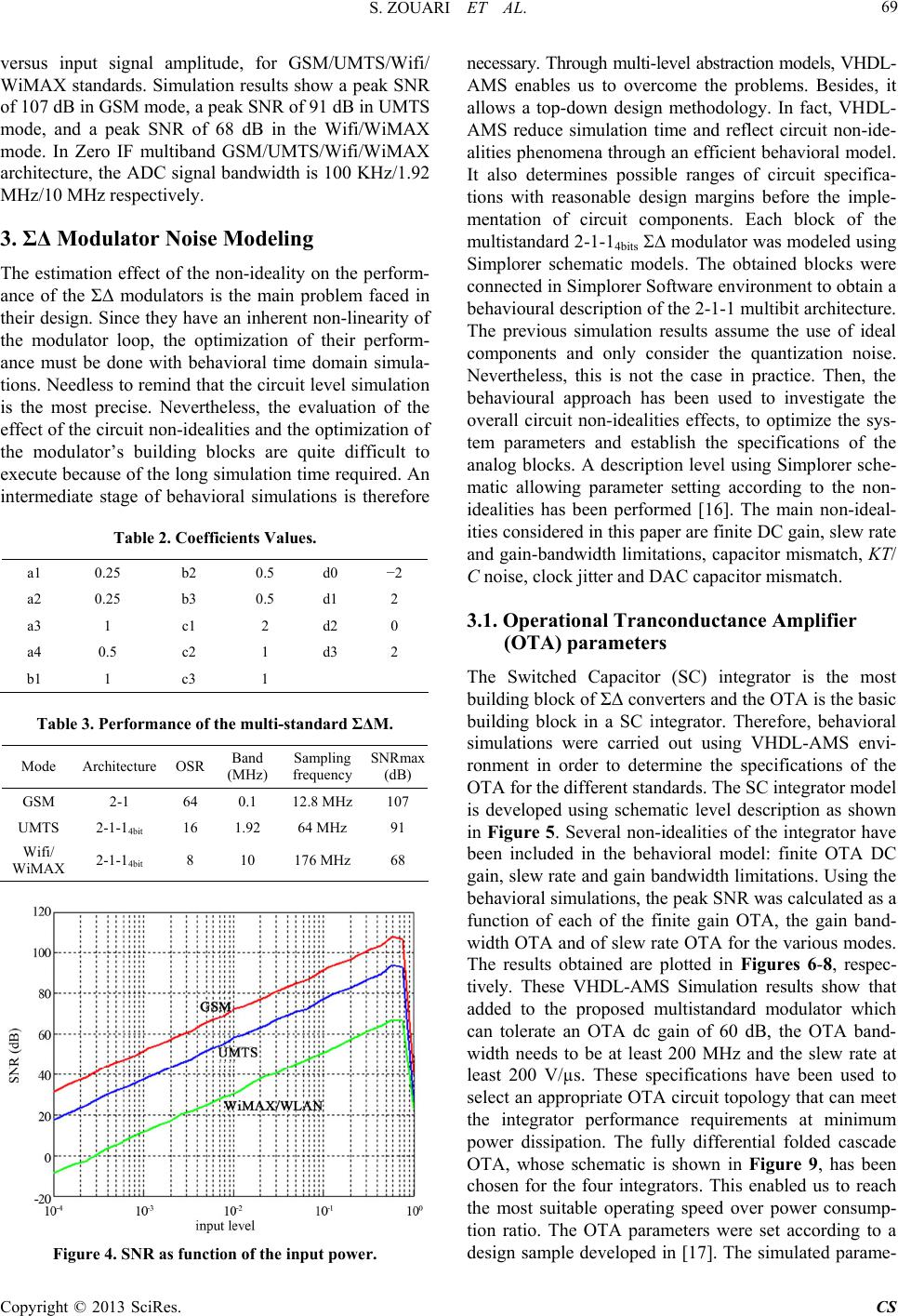
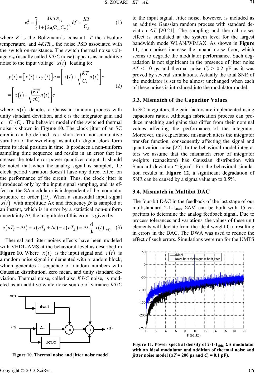
the modulator output spectrum for
GSM/UMTS/Wifi/WiMAX modes for a 0.1/1.92/10 MHz
input signal at a sampling frequency of 12.8/64/176 MHz
under the condition of 0.2% random capacitor mismatch,
0.5% DAC INL mismatch. Jitter and thermal noises are
the other limitations assumed in this simulation with
clock jitter of 10 ps and Cs equal to 0.25 pF. Taking into
account the use of the real selected folded cascode OTA
in the four integrators of the reconfigurable ΣΔM, these
simulation results show that a high linearity can be
achieved thanks to the low-distortion of the Sigma-Delta
modulator. Behavioral simulation results indicate that the
proposed multistandard topology achieves a peak SNR of
105/98/65 dB for GSM/WCDMA/WLAN standards re-
spectively in the presence of these circuit non-idealities.
5. Conclusion
The major contribution of this work is the development
of an accurate behavioral model of multistandard ΣΔM
for GSM/UMTS/Wifi/WiMAX zero-IF receiver using
VHDL-AMS as the modeling language. It takes into ac-
count at the behavioural level most of SC ΣΔ modulator
non-idealities, such as DAC non-linearity, OTA parame-
ters (finite DC gain, finite bandwidth, slew rate), thermal
noise and capacitor mismatch, thus it permits to obtain a
good estimation of the ΣΔ modulator performance with a
short simulation time. Future works would involve the
implementation of the 2-1-1 cascade ΣΔ converter using
device-level simulations.
REFERENCES
[1] P.-I. Mak, U. Seng-Pan and R. P. Martins, “Transceiver
Architecture Selection: Review, State-of-the-Art Survey
and Case Study,” IEEE Circuits and Systems Magazine,
Vol. 7, No. 2, 2007, pp. 6-25.
doi:10.1109/MCAS.2007.4299439
[2] P. B. Kenington and L. Astier, “Power Consumption of
A/D Converters for Software Radio Applications,” IEEE
Transactions on Vehicular Technology, Vol. 49, No. 2,
2000, pp. 643-650. doi:10.1109/25.832996
[3] Z. Ru, N. A. Moseley, E. Klumperink and B. Nauta,
“Digitally Enhanced Software-Defined Radio Receiver
Robust to Out-of-Band Interference,” IEEE Journal of
Solid-State Circuits, Vol. 44, No. 12, 2009, pp. 3359-
3375. doi:10.1109/JSSC.2009.2032272
[4] B. Razavi, “Cognitive Radio Design Challenges and
Techniques,” IEEE Journal of Solid-State Circuits, Vol.
45, No. 8, 2010, pp. 1542-1553.
doi:10.1109/JSSC.2010.2049790
[5] R. Bagheri, A. Mirzaei, M. E. Heidari, S. Chehrazi, M.
Lee, M. Mikhemar, W. K. Tang and A. A. Abidi, “Soft-
ware-Defined Radio Receiver: Dream to Reality,” IEEE
Communications Magazine, Vol. 44, No. 8, 2006, pp.
111-118. doi:10.1109/MCOM.2006.1678118
[6] A. Silva, J. Guilherme and N. Horta, “Reconfigurable
Multi-Mode Sigma-Delta Modulator for 4G Mobile Ter-
minals,” Integration, the VLSI Journal, Vol. 42, No. 1,
2009, pp. 34-46.
[7] M. Miller and C. Petrie, “A Multibit Sigma Delta ADC
for Multimode Receivers,” IEEE Journal of Solid State
Circuits, Vol. 38, No. 3, 2003, pp. 475-482.
doi:10.1109/JSSC.2002.808321
[8] F. Medeiro, B. Pérez-Verdú and A. Rodríguez-Vázquez,
“Top-Down Design of High-Performance Sigma-Delta
Modulators,” Kluwer Academic Publishers, Boston, 1999,
p. 312.
[9] A. A. Abidi, “The Path to the Software-Defined Radio
Receiver,” IEEE Journal of Solid-State Circuits, Vol. 42,
No. 5, 2007, pp. 954-966. doi:10.1109/JSSC.2007.894307
[10] N. Ghittori, A. Vigna, P. Malcovati, S. D’Amico and A.
Baschirotto, “Analogbaseband Channel for Reconfigur-
able Multistandard (GSM/UMTS/WLAN/Bluetooth) Re-
ceivers,” Proceedings of the WIRTEP, Rome, April 2006,
pp. 88-92.
[11] M. Brandolini, P. Rossi, D. Manstretta and F. Svelto,
“Toward Multistandard Mobile Terminals—Fully Inte-
grated Receivers Requirements and Architectures,” IEEE
Transactions on Microwave Theory and Techniques, Vol.
53, No. 3, 2005, pp. 1026-1038.
doi:10.1109/TMTT.2005.843505
[12] R. del Río, F. Medeiro, J. M. de la Rosa, B. Pérez-Verdú
and A. Rodríguez-Vázquez, “A 2.5 V CMOS Wideband
Sigma-Delta Modulator,” IEEE Instrumentation and
Measurement Technology Conference, Vail Colorado,
May 2003, pp. 224-228.
[13] A. Silva, J. Guilherme and N. HortaCir, “A Reconfigur-
able Sigma-Delta Modulator Reconfiguration of Cascade
Sigma Delta Modulators for Multistandard GSM/Blue-
tooth/UMTS/WLAN Transceivers,” IEEE International
Symposium on Integration Circuits and Systems, ISCAS,
Island of Kos, 21-24 May 2006, pp. 1884-1887.
[14] J. Marttila, M. Allén and M. Valkama, “Design and
Analysis of Multi-Stage Quadrature Sigma-Delta A/D
Converter for Cognitive Radio Receivers,” Proceedings
of the 16th IEEE International Workshop on Computer-
Aided Modeling Analysis and Design of Communication
Links and Networks, Kyoto, 10-11 June 2011, pp. 10-11.
[15] A. Morgado, R. del Río and J. M. de la Rosa, “Design of
a 130-nm CMOS Reconfigurable Cascade ΣΔ Modulator
for GSM/UMTS/Bluetooth,” IEEE International Sympo-
sium on Circuits and Systems, ISCAS, Island of Kos,
27-30 May 2007, pp. 725-728.
[16] S. zouari, et al., “High Order Cascade Multibit Sigma
Delta Modulator for Wide Bandwidth Applications,” In-
ternational Journal of Electronic Commerce Studies, Vol.
1, No. 1, 2007, pp. 60-66.
[17] H. Daoud, S. Bennour, S. Ben Salem and M. Loulou,
“Low Power SC CMFB Folded Cascode OTA Optimiz-
tion,” The IEEE International Conference on Electronics,
Circuits, and Systems, St. Julien, 31 August-3 September
2008, pp. 570-573.
[18] R. Schreier, J. Silva, J. Steensgaard and G. C. Temes
“Design-Oriented Estimation of Thermal Noise in Swit-
ched-Capacitor Circuits,” IEEE Transactions on Circuits
Copyright © 2013 SciRes. CS
S. ZOUARI ET AL.
Copyright © 2013 SciRes. CS
74
and Systems: Regular Papers, Vol. 52, 2005, pp. 2358-
2368.
[19] Y. Yin, H. Klar and P. Wennekers, “A Cascade 3-1-1
Multibit ΣΔ Modulator with Reduced Sensitities to Non-
Idealities,” The IEEE International Symposium on Cir-
cuits and Systems, Vol. 4, 2005, pp. 3087-3090.
[20] Y. B. N. Kumar, S. Talay and F. Maloberti, “Complex
Cascaded Bandpass ΣΔ ADC Design,” Proceedings of the
IEEE International Symposium on Circuits and Systems,
Taipei, 24-27 May 2009, pp. 3118-3121.
[21] Van Tam, “VHDL-AMS Behavioral Modelling and
Simulation of High-Pass Delta-Sigma Modulator,” IEEE
Transactions on Circuits and Systems I: Fundamental
Theory and Applications, Vol. 50, No. 3, 2005, pp. 352-
364.
[22] P. Malcovati, S. Brigati, F. Francesconi, F. Maloberti, P.
Cusinato and A. Baschirotto, “Behavioral Modeling of
Switched-Capacitor Sigma-Delta Modulators,” IEEE In-
ternational Symposium on Circuits and Systems, Vol. 50,
2003, pp. 352-364.