Circuits and Systems, 2013, 4, 11-15
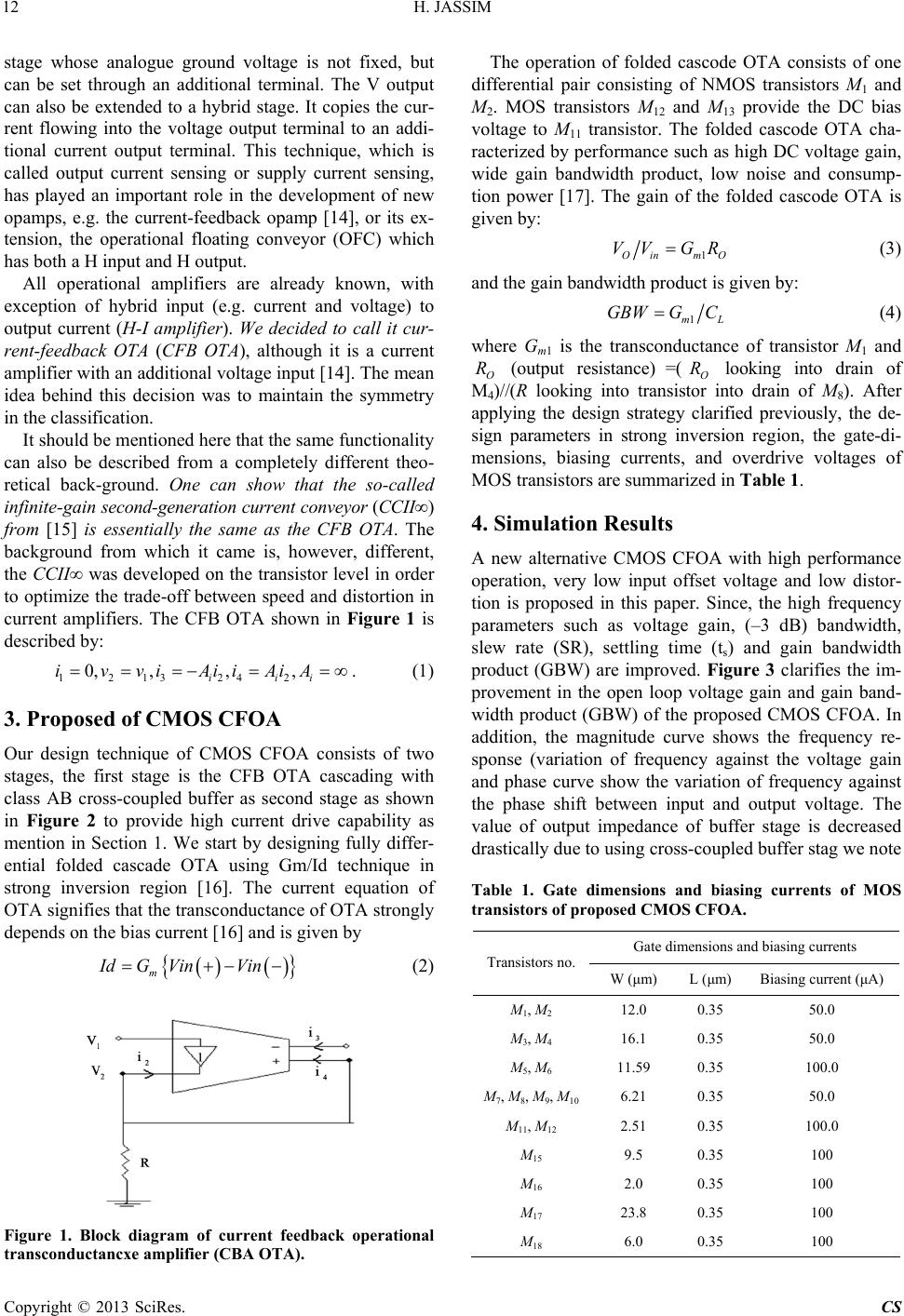
http://dx.doi.org/10.4236/cs.2013.41003 Published Online January 2013 (http://www.scirp.org/journal/cs)
A New Design Technique of CMOS Current Feed Back
Operational Amplifier (CFOA)
Hassan Jassim
Department of Electrical Engineering, College of Engineering, Babylon University, Babylon, Iraq
Email: hssn_jasim@yahoo.com
Received September 14, 2012; revised October 29, 2012; accepted November 6, 2012
ABSTRACT
A new design technique employing CMOS Current Feedback Operational Amplifier (CFOA) is presented. This design
approach applies CFA OTA as input stage cascaded with class AB cross-coupled buffer stage. The performance pa-
rameters of CMOS CFOA such as bandwidth, slew rate, settling time are extensively improved compared with conven-
tional CFOA. These parameters are very important in high frequency applications that use CMOS CFOA as an active
building block such as A/D converters, and active filters. Also the DC input offset voltage and harmonic distortion (HD)
are very low values compared with the conventional CMOS CFOA are obtained. P-Spice simulation results using 0.35
µm MI-ETEC CMOS process parameters shows considerable improvement over existing CMOS CFOA simulated
model. Some of the performance parameters for example are DC gain of 67.2 dB, open-loop gain bandwidth product of
104 MHz, slew rate (SR+) of +91.3 V/µS, THD of 67 dB and DC input offset voltage of 0.2 mV.
Keywords: Synthesis CFA OTA and CMOS CFOA; Cross Coupled Buffer Stage; High Performance CFOA; Low
Input Offset Voltage CFOA; Low Distortion CFOA
1. Introduction
The role of analog integrated circuits in modem elec-
tronic systems remains important, even though digital
circuits dominate the market for VLSI solutions. Analog
systems have always played an essential role in interface-
ing digital electronics to the real world in applications
such as analog signal processing and conditioning, in-
dustrial process, motion control and biomedical meas-
urements [1]. However, the conventional CMOS CFOA
design is still facing certain problems, first, the offset
voltage on the current feedback can not be made zero.
CFOA usually adopts an analog buffer as the input stage.
As a result, the non-inverting input has very high im-
pedance, while the inverting input has very low imped-
ance. Hence, the CFOAs offset is higher than folded
cascade voltage amplifier (VFA) Design. Second, the
constant bandwidth feature of the CFOA is only ap-
proximate if the inverting input impedance is not small
enough [2,3]. The low-input offset voltage is considered
as an important aspect of the performance of an amplifier
especially when signals are in the range of few hundred
micro volts [4]. Several CMOS realizations for the
CFOA have been reported in the literature [5-12]. The
design still suffers from many drawbacks such as high
distortion, high noise, high consumption of power and
complex circuitry. The CFOA has been always seen as
an extension of the CCII, therefore, the design approach
was cascade with CCII+ with a voltage follower to real-
ize a complete circuit. The obtained bandwidth was al-
ways the degraded version of CCII+.
The current feedback operational amplifier (CFOA), a
two-port (four-terminal) network. The CFOA could be
realized by using second generation current conveyor
CCII+ cascaded with a voltage follower [13].
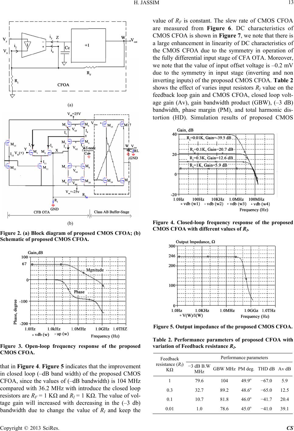
This paper describes an alternative approach to CMOS
CFOA design which provides symmetrical high imped-
ances (infinite for DC) inputs together with high per-
formance parameters in high frequency operation. This
design approach applies CFA OTA as input stage cas-
caded with class AB cross-coupled buffer as output stage.
The symmetrical input stage of CFA OTA will reduce
the DC offset voltage of CMOS CFOA with improve-
ment of high frequency parameters. Moreover, class AB
cross coupled buffer stage provide high current drive
capability. P-Spice simulation results confirm the theo-
retical calculations.
2. Theoretical Background of CFB OTA
The two output terminals are not seen as one port each,
but as four independent terminals that can have different
impedance levels. As a consequence, hybrid stages ap-
pear, namely a H input stage and a H output stage. The H
input stage, which has become well known through the
CFB opamp, can also be understood as an extended input
C
opyright © 2013 SciRes. CS
H. JASSIM
12
stage whose analogue ground voltage is not fixed, but
can be set through an additional terminal. The V output
can also be extended to a hybrid stage. It copies the cur-
rent flowing into the voltage output terminal to an addi-
tional current output terminal. This technique, which is
called output current sensing or supply current sensing,
has played an important role in the development of new
opamps, e.g. the current-feedback opamp [14], or its ex-
tension, the operational floating conveyor (OFC) which
has both a H input and H output.
All operational amplifiers are already known, with
exception of hybrid input (e.g. current and voltage) to
output current (H-I amplifier). We decided to call it cur-
rent-feedback OTA (CFB OTA), although it is a current
amplifier with an additional voltage input [14]. The mean
idea behind this decision was to maintain the symmetry
in the classification.
It should be mentioned here that the same functionality
can also be described from a completely different theo-
retical back-ground. One can show that the so-called
infinite-gain second-generation current conveyor (CCII)
from [15] is essentially the same as the CFB OTA. The
background from which it came is, however, different,
the CCII was developed on the transistor level in order
to optimize the trade-off between speed and distortion in
current amplifiers. The CFB OTA shown in Figure 1 is
described by:
1213 2
0, ,,ivviAi42
,
iii
iAiA 
 

Vin
. (1)
3. Proposed of CMOS CFOA
Our design technique of CMOS CFOA consists of two
stages, the first stage is the CFB OTA cascading with
class AB cross-coupled buffer as second stage as shown
in Figure 2 to provide high current drive capability as
mention in Section 1. We start by designing fully differ-
ential folded cascade OTA using Gm/Id technique in
strong inversion region [16]. The current equation of
OTA signifies that the transconductance of OTA strongly
depends on the bias current [16] and is given by
m
IdG Vin (2)
Figure 1. Block diagram of current feedback operational
transconductancxe amplifier (CBA OTA).
The operation of folded cascode OTA consists of one
differential pair consisting of NMOS transistors M1 and
M2. MOS transistors M12 and M13 provide the DC bias
voltage to M11 transistor. The folded cascode OTA cha-
racterized by performance such as high DC voltage gain,
wide gain bandwidth product, low noise and consump-
tion power [17]. The gain of the folded cascode OTA is
given by:
1Oin mO
VV GR (3)
and the gain bandwidth product is given by:
1mL
GBWGC (4)
where Gm1 is the transconductance of transistor M1 and
O (output resistance) =( O looking into drain of
M4)//(R looking into transistor into drain of M8). After
applying the design strategy clarified previously, the de-
sign parameters in strong inversion region, the gate-di-
mensions, biasing currents, and overdrive voltages of
MOS transistors are summarized in Table 1.
R R
4. Simulation Results
A new alternative CMOS CFOA with high performance
operation, very low input offset voltage and low distor-
tion is proposed in this paper. Since, the high frequency
parameters such as voltage gain, (–3 dB) bandwidth,
slew rate (SR), settling time (ts) and gain bandwidth
product (GBW) are improved. Figure 3 clarifies the im-
provement in the open loop voltage gain and gain band-
width product (GBW) of the proposed CMOS CFOA. In
addition, the magnitude curve shows the frequency re-
sponse (variation of frequency against the voltage gain
and phase curve show the variation of frequency against
the phase shift between input and output voltage. The
value of output impedance of buffer stage is decreased
drastically due to using cross-coupled buffer stag we note
Table 1. Gate dimensions and biasing currents of MOS
transistors of proposed CMOS CFOA.
Gate dimensions and biasing currents
Transistors no.
W (μm) L (μm) Biasing current (μA)
M1, M2 12.0 0.35 50.0
M3, M4 16.1 0.35 50.0
M5, M6 11.59 0.35 100.0
M7, M8, M9, M10 6.21 0.35 50.0
M11, M12 2.51 0.35 100.0
M15 9.5 0.35 100
M16 2.0 0.35 100
M17 23.8 0.35 100
M18 6.0 0.35 100
Copyright © 2013 SciRes. CS
H. JASSIM 13
(a)
(b)
Figure 2. (a) Block diagram of proposed CMOS CFOA; (b)
Schematic of proposed CMOS CFOA.
Figure 3. Open-loop frequency response of the proposed
CMOS CFOA.
that in Figure 4. Figure 5 indicates that the improvement
in closed loop (–dB band width) of the proposed CMOS
CFOA, since the values of (–dB bandwidth) is 104 MHz
compared with 36.2 MHz with introduce the closed loop
resistors are RF = 1 K and RI = 1 K. The value of vol-
tage gain will increased with decreasing in the (–3 db)
bandwidth due to change the value of RI and keep the
value of RF is constant. The slew rate of CMOS CFOA
are measured from Figure 6. DC characteristics of
CMOS CFOA is shown in Figure 7, we note that there is
a large enhancement in linearity of DC characteristics of
the CMOS CFOA due to the symmetry in operation of
the fully differential input stage of CFA OTA. Moreover,
we note that the value of input offset voltage is –0.2 mV
due to the symmetry in input stage (inverting and non
inverting inputs) of the proposed CMOS CFOA. Table 2
shows the effect of varies input resistors RI value on the
feedback loop gain and CMOS CFOA, closed loop volt-
age gain (Av), gain bandwidth product (GBW), (–3 dB)
bandwidth, phase margin (PM), and total harmonic dis-
tortion (HD). Simulation results of proposed CMOS
Figure 4. Closed-loop frequency response of the proposed
CMOS CFOA with different values of RI.
Figure 5. Output impedance of the proposed CMOS CFOA.
Table 2. Performance parameters of proposed CFOA with
variation of Feedback resistance RI.
Performance parameters
Feedback
resistance (RI)
K 3 dB B.W
MHz GBW MHz PM deg. THD dBAv dB
1 79.6 104 49.9o 67.05.9
0.3 32.7 89.2 48.6o 65.0 12.5
0.1 10.7 81.8 46.0o 41.7 20.4
0.01 1.0 78.6 45.0o 41.0 39.1
Copyright © 2013 SciRes. CS
H. JASSIM
14
CFOA confirmed the theoretical concepts in previous
sections.
Table 3 Summarizes the comparison between several
previous works and the proposed CFOA, we note there
are a considerable improvement of performance parame-
ters of proposed CFOA compared with previous works.
Specially high frequency parameters, harmonic distortion
and input offset voltage.
Figure 6. 1V Step response of the CMOS CFOA using (CL)
= 10 PF.
Figure 7. DC Characteristics of the CMOS CFOA with RL =
1 K.
Table 3. Summarize the comparison between several works.
Reference [1] [2] [13]
Proposed
CFOA
VDD, VSS 1.5 V 3.3 V 0.75 V 2.5
Power dissipation 0.45 mW 5.3 mW 0..456 mW 5.5 mW
GBW 120 MHz 58 MHz 120 MHz 104 MHz
Input offset
voltage <20 mV 1.3 mV <20 mV 0.2 mV
DC gain - 74 dB - 67 dB
Input voltage
dynamic range
0.65 V to
+0.65 V - 0.65 V to
+0.65 V
1 V to
+1V
THD - 83 dB - 67 dB
Technology 0.25 µm 0.35 µm 0.25 µm 0.35 µm
5. Conclusion
A new design technique of the CMOS CFOA with at-
tractive features for high frequency, low offset voltage
and low distortion is proposed in this paper. The pro-
posed design based on cross-coupled buffer stage that
connected as output stage of the CMOS CFOA. Since
this technique operates on logic transition concept which
gives the high speed, symmetry operation of the output
signal and high current drive capability of proposed
CMO CFOA. The high speed operation improved high
performance parameters such as gain bandwidth (GBW),
(–3 dB) bandwidth, slew rate (SR) and settling time (ts)
with ensure the phase margin (PM) in acceptable value
that keep the stability of operation. Moreover, the sym-
metry of input differential of folded cacode CFA OTA
technique decreased the distortion in output signal and
improved (DC) characteristics of CMOS CFOA. In addi-
tion to that using folded cascode OTA (FC-OTA) as the
input stage of CMOS CFOA make the symmetry of in-
verting and non inverting inputs that reduce input offset
voltage. The trans-impedance node (Z) of the CMOS
CFOA gained high value due to cascoding transistors of
CFA OTA. This feature is very important for design
CMOS CFOA with high gain. We can summarize our
conclusion by saying that the proposed CMOS CFOA
with symmetry of the input stage and symmetry of the
output stage will gain CMOS CFOA attractive features
for many high frequency, low distortion, low input offset
voltage applications such as (A/D) converters, switched
capacitor filters, active filters.
REFERENCES
[1] A. H. Madian, S. A. Mahmoud and A. M. Soliman, “Con-
figurable Analog Block Based on CFOA and Its Applica-
tion,” WSEAS Transactions on Electronics, Vol. 5, No. 6,
2008, pp. 220-225.
[2] S. Pennisi, “High-Performance CMOS Current Feedback
Operational Amplifier,” IEEE International Symposium
on Circuits and Systems, Vol. 2, 2005, pp. 1573-1576.
[3] H. L. Chao and D. S. Ma, “CMOS Variable-Gain Wide-
Bandwidth CMFB-Free Differential Current Feedback
Amplifier for Ultrasound Diagnostic Applications,” IEEE
International Symposium on Circuits and Systems, Island
of Kos, 21-24 May 2006, pp. 649-652.
[4] G. Giustolisi, G. Palmisano, G. Palumbo and S. Pennisi,
“High-Drive CMOS Current-Feedback Opamp,” IEEE
International Symposium on Circuits and Systems, Sac-
ramento, 3-6 August 1997, pp. 229-232.
[5] J. Mahattanakul and C. Toumazou, “A Theoretical Study
of the Stability of High Frequency Current Feedback
Op-Amp Integrators,” IEEE Transactions on Circuits and
Systems, Vol. 43, No.1, 1996, pp. 1-12.
[6] G. Di Cataldo, A. D. Grasso and S. Pennisi, “Two CMOS
Current Feedback Operational Amplifiers,” IEEE Trans-
Copyright © 2013 SciRes. CS
H. JASSIM
Copyright © 2013 SciRes. CS
15
actions on Circuits and Systems, Vol. 54, No. 11, 2007,
pp. 1-5.
[7] A. Assi, M. Sawan and J. Zhu, “An Offset Compensated
and High-Gain CMOS Current-Feedback Op-Amp,”
IEEE Transaction on Circuits and Systems, Vol. 45, No.
1, 1998. pp. 85-90. doi:10.1109/81.660763
[8] A. M. Ismail and A. M. Soliman, “Novel CMOS Current
Feedback Op-Amp Realization Suitable for High Fre-
quency Applications,” IEEE Transaction on Circuits and
Systems, Vol. 47, No. 6, 2000, pp. 918-921.
doi:10.1109/81.852946
[9] S. Selvanayagam and F. J. Lidgey, “Wide Bandwidth
CMOS Current Feedback Op-Amp for Inverting Applica-
tions,” IEEE Electronics Letters Journal, London, 10
May 1996, pp. 1-4.
[10] J. Y. Zhu, M. Sawan and K. Arabi, “An Offset Compen-
sated CMOS Current-Feedback Operational Amplifier,”
IEEE International Symposium on Circuits and Systems,
Seattle, 30 April-3 May1995, pp. 1552-1555.
[11] G. Palumbo and S. Pennisi, “Current-Feedback Amplifi-
ers versus Voltage Operational Amplifiers,” IEEE Trans-
action on Circuits and Systems, Vol. 48, No. 5, 2001, pp.
617-623. doi:10.1109/81.922465
[12] M. Djebbi, A. Assi and M. Sawan, “An Offset-Compen-
sated Wide-Bandwidth CMOS Current-Feedback Opera-
tional Amplifier,” IEEE International Symposium on
Circuits and Systems, Vol. 1, 2003, pp. 73-76.
[13] S. A. Mahmoud, A. H. Madian and A. M. Soliman,
“Low-Voltage CMOS Current Feedback Operational
Amplifier and Its Applications,” ETRI Journal, Vol. 29,
No. 2, 2007, pp. 655-658.
[14] H. Schmid, “The Current-Feedback OTA,” IEEE Interna-
tional Symposium on Circuits and Systems, Sydney, 6-9
May 2001, pp. 655-658.
[15] K. Koli, “CMOS Current Amplifiers: Speed versus
Nonlinearity,” Ph.D. Thesis, Dissertation in Department
of Electrical and Communication Engineering, Helsiniki
University of Technology, Espoo, 2000.
[16] P. E. Allen and D. R. Holberg, “CMOS Analog Circuit
Design,” 2nd Edition, Oxford University Press, New
York, 2004.
[17] T. Singh, M. Kaur and G. Singh, “Design and Analysis of
CMOS Folded-Cascode OTA Using Gm/Id Tecghnique,”
International Journal of Electronics and Computer Sci-
ence Engineering, Vol. 1, No. 2, 2012, pp. 727-733.