J. VAN VEEN ET AL.
16
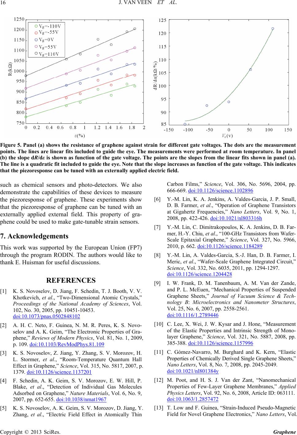
Figure 5. Panel (a) shows the resistance of graphene against strain for different gate voltages. The dots are the measurement
points. The lines are linear fits included to guide the eye. The measurements were performed at room temperature. In panel
(b) the slope dR/dε is shown as function of the gate voltage. The points are the slopes from the linear fits shown in panel (a).
The line is a quadratic fit included to guide the eye. Note that the slope increases as function of the gate voltage. This indicates
that the piezoresponse can be tuned with an externally applied electric field.
such as chemical sensors and photo-detectors. We also
demonstrate the capabilities of these devices to measure
the piezoresponse of graphene. These experiments show
that the piezoresponse of graphene can be tuned with an
externally applied external field. This property of gra-
phene could be used to make gate-tunable strain sensors.
7. Acknowledgements
This work was supported by the European Union (FP7)
through the program RODIN. The authors would like to
thank E. Huisman for useful discussions.
REFERENCES
[1] K. S. Novoselov, D. Jiang, F. Schedin, T. J. Booth, V. V.
Khotkevich, et al., “Two-Dimensional Atomic Crystals,”
Proceedings of the National Academy of Sciences, Vol.
102, No. 30, 2005, pp. 10451-10453.
doi:10.1073/pnas.0502848102
[2] A. H. C. Neto, F. Guinea, N. M. R. Peres, K. S. Novo-
selov and A. K. Geim, “The Electronic Properties of Gra-
phene,” Reviews of Modern Physics, Vol. 81, No. 1, 2009,
p. 109. doi:10.1103/RevModPhys.81.109
[3] K. S. Novoselov, Z. Jiang, Y. Zhang, S. V. Morozov, H.
L. Stormer, et al., “Room-Temperature Quantum Hall
Effect in Graphene,” Science, Vol. 315, No. 5817, 2007, p.
1379. doi:10.1126/science.1137201
[4] F. Schedin, A. K. Geim, S. V. Morozov, E. W. Hill, P.
Blake, et al., “Detection of Individual Gas Molecules
Adsorbed on Graphene,” Nature Materials, Vol. 6, No. 9,
2007, pp. 652-655. doi:10.1038/nmat1967
[5] K. S. Novoselov, A. K. Geim, S. V. Morozov, D. Jiang, Y.
Zhang, et al., “Electric Field Effect in Atomically Thin
Carbon Films,” Science, Vol. 306, No. 5696, 2004, pp.
666-669. doi:10.1126/science.1102896
[6] Y.-M. Lin, K. A. Jenkins, A. Valdes-Garcia, J. P. Small,
D. B. Farmer, et al., “Operation of Graphene Transistors
at Gigahertz Frequencies,” Nano Letters, Vol. 9, No. 1,
2008, pp. 422-426. doi:10.1021/nl803316h
[7] Y.-M. Lin, C. Dimitrakopoulos, K. A. Jenkins, D. B. Far-
mer, H.-Y. Chiu, et al., “100-GHz Transistors from Wafer-
Scale Epitaxial Graphene,” Science, Vol. 327, No. 5966,
2010, p. 662. doi:10.1126/science.1184289
[8] Y.-M. Lin, A. Valdes-Garcia, S.-J. Han, D. B. Farmer, I.
Meric, et al., “Wafer-Scale Graphene Integrated Circuit,”
Science, Vol. 332, No. 6035, 2011, pp. 1294-1297.
doi:10.1126/science.1204428
[9] I. W. Frank, D. M. Tanenbaum, A. M. Van der Zande,
and P. L. McEuen, “Mechanical Properties of Suspended
Graphene Sheets,” Journal of Vacuum Science & Tech-
nology B: Microelectronics and Nanometer Structures,
Vol. 25, No. 6, 2007, pp. 2558-2561.
doi:10.1116/1.2789446
[10] C. Lee, X. Wei, J. W. Kysar and J. Hone, “Measurement
of the Elastic Properties and Intrinsic Strength of Mono-
layer Graphene,” Science, Vol. 321, No. 5887, 2008, pp.
385-388. doi:10.1126/science.1157996
[11] C. Gómez-Navarro, M. Burghard and K. Kern, “Elastic
Properties of Chemically Derived Single Graphene Sheets,”
Nano Letters, Vol. 8, No. 7, 2008, pp. 2045-2049.
doi:10.1021/nl801384y
[12] M. Poot, and H. S. J. Van der Zant, “Nanomechanical
Properties of Few-Layer Graphene Membranes,” Applied
Physics Letters, Vol. 92, No. 6, 2008, Article ID: 063111.
doi:10.1063/1.2857472
[13] T. Low and F. Guinea, “Strain-Induced Pseudo-Magnetic
Field for Novel Graphene Electronics,” Nano Letters, Vol.
Copyright © 2013 SciRes. Graphene