Z. XIONG, W. WU
Copyright © 2013 SciRes. MNSMS
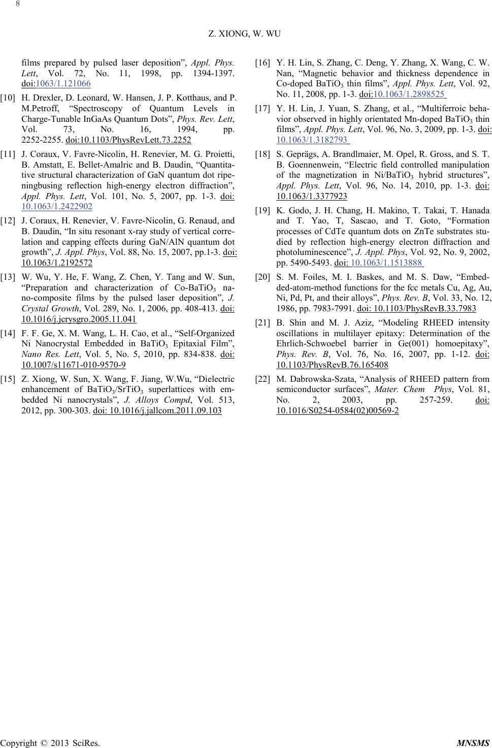
every separate layer is accurately controlled by RHEED
intensity oscillation which is extremely sensitive to the
presence of surface atoms in the top crystalline layer [3].
The individual BTO layer and STO layer have the uni-
form thickness of 14nm and 21nm, respectively. Ac-
cording to the results of RHEED monitored, the growth
rate of STO and BTO are estimated to be 0.037 ML/s and
0.043 ML/s, where 1 monolayer (ML) corresponds to a
layer thickness of 0.781 nm (STO) and 0.806 nm (BTO),
the double value of the c-axis lattice constant of bulk
STO (0.3905 nm) and BTO (0.4029 nm) [5], respectively.
So it is concluded that one period of RHEED intensity
oscillation corresponds to the growth of two STO unit
cells and two BTO unit cells, respectively. We achieve
atomic-level control for the growth of the nanocomposite
fil m.
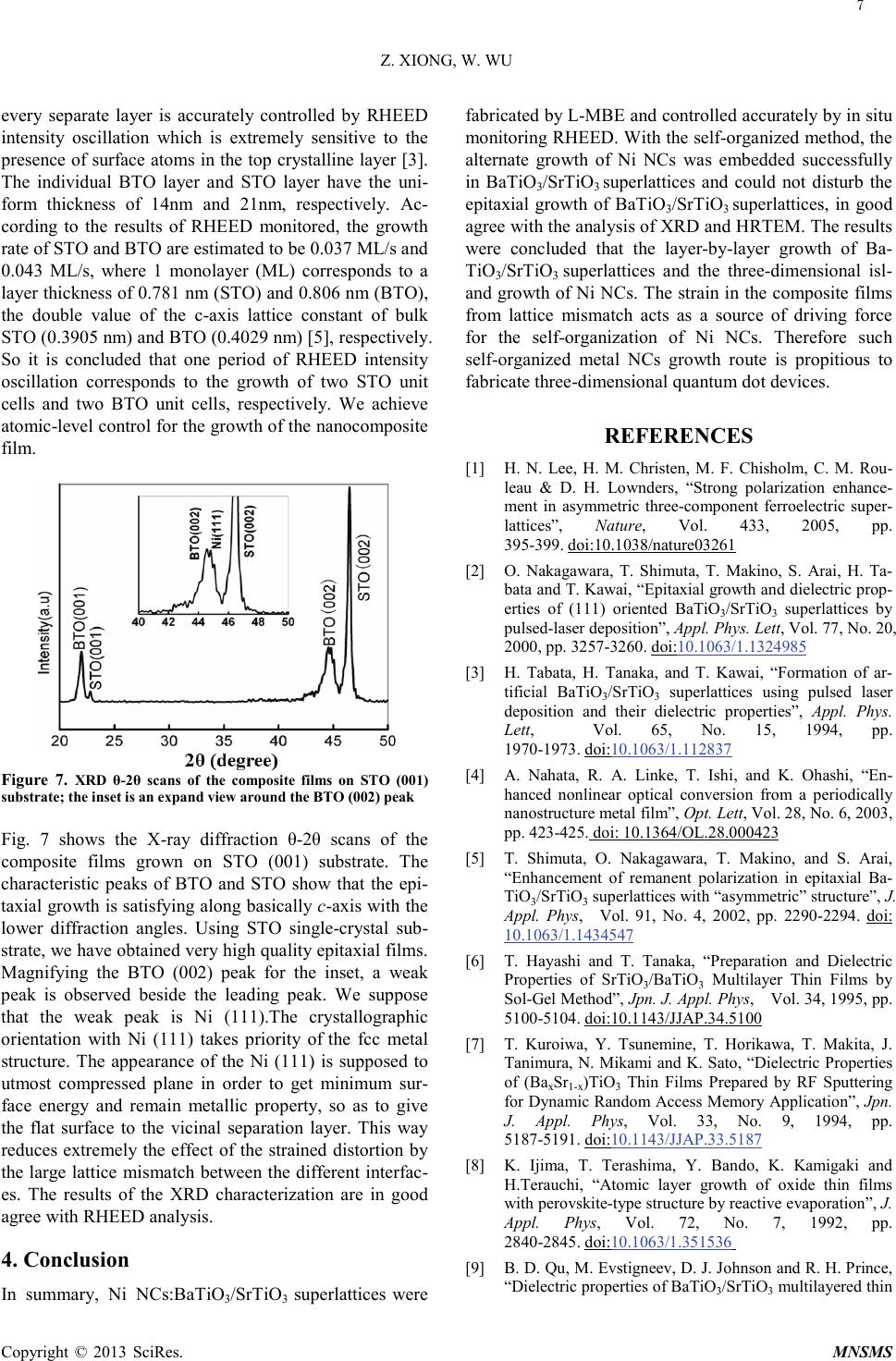
Figure 7. XRD θ-2θ scans of the composite films on STO (001)
substrate; the inset is an expand view around the BTO (002) peak
Fig. 7 shows the X-ray diffraction θ-2θ scans of the
composite films grown on STO (001) substrate. The
characteristic peaks of BTO and STO show that the epi-
taxial growth is satisfying along basically c-axis with the
lower diffraction angles. Using STO single-crystal sub-
strate, we have obtained very high quality epitaxial films.
Magnifying the BTO (002) peak for the inset, a weak
peak is observed beside the leading peak. We suppose
that the weak peak is Ni (111).The crystallographic
orientation with Ni (111) takes priority of the fcc metal
structure. The appearance of the Ni (111) is supposed to
utmost compressed plane in order to get minimum sur-
face energy and remain metallic property, so as to give
the flat surface to the vicinal separation layer. This way
reduces extremely the effect of the strained distortion by
the large lattice mismatch between the different interfac-
es. The results of the XRD characterization are in good
agree with RHEED analysis.
4. Conclusion
In summary, Ni NCs:BaTiO3/SrTiO3 superlattices were
fabricated by L-MBE and controlled accurately by in situ
monitoring RHEED. With the self-or ga nized method, the
alternate growth of Ni NCs was embedded successfully
in BaTiO3/SrTiO3 superlattices and could not disturb the
epitaxial growth of BaTiO3/SrTiO3 superlattices, in good
agree with the anal ysi s of XRD and HRTEM. The results
wer e concluded that the layer-by-layer growth of Ba-
TiO3/SrTiO3 superlattices and the t hree -dimensional isl-
and growth of Ni NCs. The strain in the composite films
from lattice mismatch acts as a source of driving force
for the self-organization of Ni NCs. Therefore such
self-or ga nized metal NCs growth route is propitious to
fabricate three -di mensio nal quantum dot devices.
REFERENCES
[1] H. N. Lee, H. M. Christen, M. F. Chisholm, C. M. Rou-
leau & D. H. Lownders, “Strong polarization enhance-
ment in asymmetric three-component ferroelectric super-
lattices”, Nature, Vol. 433, 2005, pp.
395-399.
[2] O. Nakagawara, T. Shimuta, T. Makino, S. Arai, H. Ta-
bata and T. Kawai, “Epitaxial growth and dielectric prop-
erties of (111) oriented BaTiO3/SrTiO3 superlattices by
pulsed-laser deposition”, Appl. Phys. Lett, Vol. 77, No. 20,
2000, pp. 3257-3260. doi:
doi:10.1038/nature03261
10.1063/1.1324985
[3] H. Tabata, H. Tanaka, and T. Kawai, “Formation of ar-
tificial BaTiO3/SrTiO3 superlattices using pulsed laser
deposition and their dielectric properties”, Appl. Phys.
Lett, Vol. 65, No. 15, 1994, pp.
1970-1973.
[4] A. Nahata, R. A. Linke, T. Ishi, and K. Ohashi, “En-
hanced nonlinear optical conversion from a periodically
nanostructure metal film”, Opt. Lett, Vol. 28, No. 6, 2003,
pp. 423-425.
doi:10.1063/1.112837
[5] T. Shimuta, O. Nakagawara, T. Makino, and S. Arai,
“Enhancement of remanent polarization in epitaxial Ba-
TiO3/SrTiO3 superlattices with “asymmetric” structure”, J.
Appl. Phys, Vol. 91, No. 4, 2002, pp. 2290-2294.
doi: 10.1364/OL.28.000423
[6] T. Hayashi and T. Tanaka, “Preparation and Dielectric
Properties of SrTiO3/BaTiO3 Multilayer Thin Films by
Sol-Gel Method”, Jpn. J. Appl. Phys, Vol. 34, 1995, pp.
5100-5104.
doi:
10.1063/1.1434547
[7] T. Kuroiwa, Y. Tsunemine, T. Horikawa, T. Makita, J.
Tanimura, N. Mikami and K. Sato, “Dielectric Properties
of (BaxSr1-x)TiO3 Thin Films Prepared by RF Sputtering
for Dynamic Random Access Memory Application”, Jpn.
J. Appl. Phys, Vol. 33, No. 9, 1994, pp.
5187-5191.
doi:10.1143/JJAP.34.5100
[8] K. Ijima, T. Terashima, Y. Bando, K. Kamigaki and
H.Terauch i, “Atomic layer growth of oxide thin films
with perovskite-type structure by reactive evaporation”, J.
Appl. Phys, Vol. 72, No. 7, 1992, pp.
2840-2845.
doi:10.1143/JJAP.33.5187
[9] B. D. Qu, M. Evstigneev, D. J. Johnson and R. H. Prince,
“Dielectric properties of BaTi O 3/SrTiO3 multilayered thin
doi:10.1063/1.351536