Paper Menu >>
Journal Menu >>
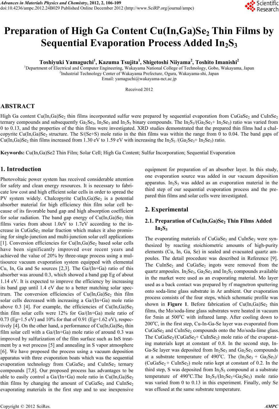 Advances in Materials Physics and Chemistry, 2012, 2, 106-109 doi:10.4236/ampc.2012.24B029 Published Online December 2012 (http://www.SciRP.org/journal/ampc) Preparation of High Ga Content Cu(In,Ga)Se2 Thin Films by Sequential Evaporation Process Added In2S3 Toshiyuki Yamaguchi1, Kazuma Tsujita1, Shigetoshi Niiyama2, Toshito Imanishi2 1Department of Electrical and Computer Engineering, Wakayama National College of Technology, Gobo, Wakayama, Japan 2Industrial Technology Center of Wakayama Prefecture, Ogura, Wakayama-shi, Japan Email: yamaguchi@wakayama-nct.ac.jp Received 2012 ABSTRACT High Ga content Cu(In,Ga)Se2 thin films incorporated sulfur were prepared by sequential evaporation from CuGaSe2 and CuInSe2 ternary compounds and subsequently Ga2Se3, In2Se3 and In2S3 binary compounds. The In2S3/(Ga2Se3+ In2Se3) ratio was varied from 0 to 0.13, and the properties of the thin films were investigated. XRD studies demonstrated that the prepared thin films had a chal- copyrite Cu(In,Ga)Se2 structure. The S/(Se+S) mole ratio in the thin films was within the range from 0 to 0.04. The band gaps of Cu(In,Ga)Se2 thin films increased from 1.30 eV to 1.59 eV with increasing the In2S3 /(Ga2Se3+ In2Se3) ratio. Keywords: Cu(In,Ga)Se2 Thin Film; Solar Cell; High Ga Content; Sulfur Incorporation; Sequential Evaporation 1. Introduction Photovoltaic power system has received considerable attention for safety and clean energy resources. It is necessary to fabri- cate low cost and high efficient solar cells in order to spread the PV system widely. Chalcopyrite Cu(In,Ga)Se2 is a potential absorber material for high efficiency thin film solar cell be- cause of its favorable band gap and high absorption coefficient for solar radiation. The band gap energy of Cu(In,Ga)Se2 thin films varies from about 1.0eV to 1.7eV according to the in- crease in CuGaSe2 molar fraction which makes it also promis- ing for single-junction and multi-junction solar cell applications [1]. Conversion efficiencies for Cu(In,Ga)Se2 based solar cells have been significantly improved over recent years and achieved the value of 20% by three-stage process using a mul- tisource vacuum evaporation system equipped with elemental Cu, In, Ga and Se sources [2,3]. The Ga/(In+Ga) ratio of this absorber was around 0.3, which showed a band gap Eg of about 1.14 eV. It is expected to improve the efficiency by increasing its band gap until 1.4 eV due to a better matching solar spec- trum. The conversion efficiencies of Cu(In,Ga)Se2 thin film solar cells decreased with increasing a Ga/(In+Ga) mole ratio above 0.3 [4]. For example, the efficiencies of Cu(In,Ga)Se2 thin film solar cells were 12% for Ga/(In+Ga) mole ratio of 0.73 (Eg=1.5 eV) and 10% for that of 0.91 (Eg=1.62 eV), respec- tively [4]. On the other hand, a performance of Cu(In,Ga)Se2 thin film solar cell with a Ga/(In+Ga) mole ratio of around 0.3 was improved by sulfurization of the film surface such as InS treat- ment by a wet process [5] and annealing in S vapor atmosphere [6]. We have proposed the process using a vacuum deposition apparatus with three evaporation boats which was the sequential evaporation technology from CuGaSe2 and CuInSe2 ternary compounds [7,8]. Our proposed process has advantages to be able to easily control a Ga/(In+Ga) mole ratio in Cu(In,Ga)Se2 thin films by changing the amount of CuGaSe2 and CuInSe2 evaporating materials in the first step and to use inexpensive equipment for preparation of an absorber layer. In this study, one evaporation source was added in our vacuum deposition apparatus. In2S3 was added as an evaporation material in the third step of our sequential evaporation process and the pre- pared thin films and solar cells were investigated. 2. Experimental 2.1. P reparation of Cu(In,Ga)Se2 Thin Films Added In2S3 The evaporating materials of CuGaSe2 and CuInSe2 were syn- thesized by reacting stoichiometric amounts of high-purity elements (Cu, In, Ga, Se) in sealed and evacuated quartz am- poules. The detail procedure was described in Reference [9]. The CuInSe2 and CuGaSe2 ingots were removed from the quartz ampoules. In2Se3, Ga2Se3 and In2S3 compounds available in the market were used as an evaporating material. Mo layer used as a back contact was prepared by rf magnetron sputtering onto soda-lime glass substrate in Ar ambient. Our evaporation process consists of the four steps, which schematic profile was shown in Figure 1. Before fabrication of Cu(In,Ga)Se2 thin films, the Mo/soda-lime glass substrates were heated in vacuum for 5min at 500oC with infrared lamp. After cooling down to 200oC, in the first step, Cu-In-Ga-Se layer was evaporated from CuGaSe2 and CuInSe2 compounds onto the Mo/soda-lime glass. The CuGaSe2/(CuGaSe2+ CuInSe2) mole ratio of the evaporat- ing materials kept at constant of 0.8. In the second step, In- Ga-Se layer was deposited from In2Se3 and Ga2Se3 compounds at a substrate temperature of 490oC. The (In2Se3 + Ga2Se3)/ (CuGaSe2 + CuInSe2) mole ratio kept at constant of 0.2. In the third step, S was deposited from In2S3 compound at a substrate temperature of 490oC.The In2S3/(In2Se3+Ga2Se3) mole ratio was varied from 0 to 0.13 in this experiment. Finally, only Se was effused at the same substrate temperature. Copyright © 2012 SciRes. AMPC 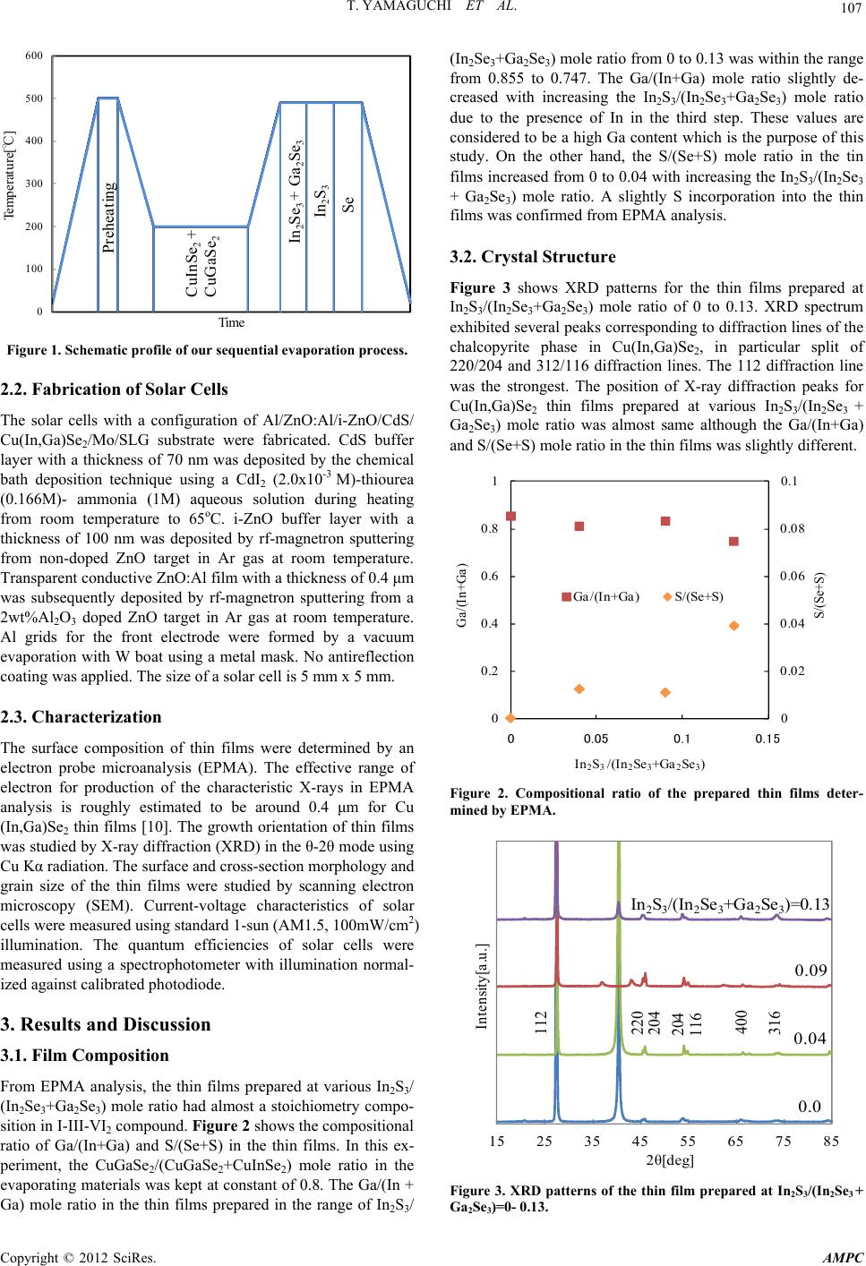 T. YAMAGUCHI ET AL. 107 0 100 200 300 400 500 600 Temperature[℃] Time CuInSe 2 + CuGaS e 2 P reheating In 2 Se 3 + Ga 2 Se 3 In 2 S 3 Se Figure 1. Schematic profile of our sequential evaporation process. 2.2. Fabricati on of Sol ar Ce l l s The solar cells with a configuration of Al/ZnO:Al/i-ZnO/CdS/ Cu(In,Ga)Se2/Mo/SLG substrate were fabricated. CdS buffer layer with a thickness of 70 nm was deposited by the chemical bath deposition technique using a CdI2 (2.0x10⁻³ M)-thiourea (0.166M)- ammonia (1M) aqueous solution during heating from room temperature to 65oC. i-ZnO buffer layer with a thickness of 100 nm was deposited by rf-magnetron sputtering from non-doped ZnO target in Ar gas at room temperature. Transparent conductive ZnO:Al film with a thickness of 0.4 μm was subsequently deposited by rf-magnetron sputtering from a 2wt%Al2O3 doped ZnO target in Ar gas at room temperature. Al grids for the front electrode were formed by a vacuum evaporation with W boat using a metal mask. No antireflection coating was applied. The size of a solar cell is 5 mm x 5 mm. 2.3. Charac t erization The surface composition of thin films were determined by an electron probe microanalysis (EPMA). The effective range of electron for production of the characteristic X-rays in EPMA analysis is roughly estimated to be around 0.4 μm for Cu (In,Ga)Se2 thin films [10]. The growth orientation of thin films was studied by X-ray diffraction (XRD) in the θ-2θ mode using Cu Kα radiation. The surface and cross-section morphology and grain size of the thin films were studied by scanning electron microscopy (SEM). Current-voltage characteristics of solar cells were measured using standard 1-sun (AM1.5, 100mW/cm2) illumination. The quantum efficiencies of solar cells were measured using a spectrophotometer with illumination normal- ized against calibrated photodiode. 3. Results and Discussion 3.1. Film Composi tion From EPMA analysis, the thin films prepared at various In2S3/ (In2Se3+Ga2Se3) mole ratio had almost a stoichiometry compo- sition in I-III-VI2 compound. Figure 2 shows the compositional ratio of Ga/(In+Ga) and S/(Se+S) in the thin films. In this ex- periment, the CuGaSe2/(CuGaSe2+CuInSe2) mole ratio in the evaporating materials was kept at constant of 0.8. The Ga/(In + Ga) mole ratio in the thin films prepared in the range of In2S3/ (In2Se3+Ga2Se3) mole ratio from 0 to 0.13 was within the range from 0.855 to 0.747. The Ga/(In+Ga) mole ratio slightly de- creased with increasing the In2S3/(In2Se3+Ga2Se3) mole ratio due to the presence of In in the third step. These values are considered to be a high Ga content which is the purpose of this study. On the other hand, the S/(Se+S) mole ratio in the tin films increased from 0 to 0.04 with increasing the In2S3/(In2Se3 + Ga2Se3) mole ratio. A slightly S incorporation into the thin films was confirmed from EPMA analysis. 3.2. Crystal Structure Figure 3 shows XRD patterns for the thin films prepared at In2S3/(In2Se3+Ga2Se3) mole ratio of 0 to 0.13. XRD spectrum exhibited several peaks corresponding to diffraction lines of the chalcopyrite phase in Cu(In,Ga)Se2, in particular split of 220/204 and 312/116 diffraction lines. The 112 diffraction line was the strongest. The position of X-ray diffraction peaks for Cu(In,Ga)Se2 thin films prepared at various In2S3/(In2Se3 + Ga2Se3) mole ratio was almost same although the Ga/(In+Ga) and S/(Se+S) mole ratio in the thin films was slightly different. 0 0.02 0.04 0.06 0.08 0.1 0 0.2 0.4 0.6 0.8 1 00.050.1 0.15 Ga /(I n+Ga ) In 2 S 3 /(In 2 Se 3 +Ga 2 Se 3 ) Ga /(I n+Ga )S/(Se+S) S/ (Se +S) Figure 2. Compositional ratio of the prepared thin films deter- mined by EPMA. 15 25 35 45 55 65 75 85 Intensity[a.u.] 2θ[deg] In 2 S 3 /(I n 2 Se 3 +Ga 2 Se 3 )=0.13 0.0 0.04 0.09 112 220 204 204 116 316 400 Figure 3. XRD patterns of the thin film prepared at In2S3/(In2Se3 + Ga2Se3)=0- 0.13. Copyright © 2012 SciRes. AMPC  T. YAMAGUCHI ET AL. 108 3.3. Grain Si ze SEM micrographs of the cross section of Cu(In,Ga)Se2 thin films prepared at In2S3/(In2Se3+Ga2Se3) mole ratio of 0 to 0.13 are shown in Figure 4. This Cu(In,Ga)Se2 thin films had a high Ga content such as Ga/(In+Ga) mole ratio of the range from 0.855 to 0.747. The grain size in Cu(In,Ga)Se2 thin film was estimated to be smaller than 1.0 μm. It is well known in general that efficiencies of polycrystalline solar cells increase with increasing grain sizes in the absorber materials. Therefore, the large grain growth in Cu(In,Ga)Se2 thin films is required for the fabrication of high-performance photovoltaic devices. In com- parison with Figures 4(a) and (b), the grain size in Figure 4(b) was seemed to be larger than that in Figure 4(a), suggesting the promotion of the grain growth by slightly In2S3 supplying. 3.4. Band gap Engineering The solar cells with a configuration of ZnO: Al/i-ZnO/CdS/Cu (In,Ga)Se2/Mo/soda-lime glass substrate were fabricated by using Cu(In,Ga)Se2 thin films prepared at In2S3/(In2Se3 + Ga2Se3) = 0-0.13. The best solar cell demonstrated Voc=500mV, Isc= 19.07mA/cm2, FF = 0.39 and η = 4.1% without AR-coating, which used Cu(In,Ga)Se2 thin film prepared at In2S3/(In2Se3 + Ga2Se3)=0.04. The efficiencies for Cu(In,Ga)Se2 thin film solar cells were not so good. However, the remarkable change was observed in the quantum efficiency of Cu(In,Ga)Se2 thin film solar cells, which was shown in Figure 5. The quantum effi- ciency from 400 nm to 600nm for Cu(In,Ga)Se2 thin film solar cells prepared at In2S3/(In2Se3+Ga2Se3) = 0.04 and 0.09 in- creased rather than that at In2S3/(In2Se3+Ga2Se3) = 0. Moreover, the absorption band edge in the long wavelength region shifted to the short wavelength range with increasing In2S3/(In2Se3+ Ga2Se3) mole ratio. For a direct transition, the dependence of the absorption coefficient α on the photon energy h is given by 12 hAhEg (1) (a) In2S3/(In2Se3+Ga2Se3)=0.0 (b) 0.04 (c) 0.09 (d) 0.13 Figure 4. SEM micrographs of the cross-section of Cu(In,Ga)Se2 thin films prepared at In2S3/(In2Se3+Ga2Se3) =0-0.13. Assuming a very short minority carrier diffusion length Ln, the quantum efficiency QE can be approximated by 1expQE W (2) where W is the width of the space charge region. From eu- qations (1) and (2), the following equation is deduced 12 ln 1QEhWA hEg (3) so that a plot of [h xIn(1-QE)]2 against h can be used to extrapolate the band gap Eg [11]. From this manner, the band gaps estimated from the QE spectra were changed from 1.30 eV to 1.59 eV, which shown in Figure 6 including the open circuit voltage Voc of Cu(In,Ga)Se2 thin film solar cells. The value of band gap is expected to be 1.56eV for Cu(In,Ga)Se2 thin film with Ga/III=0.855 from the data reported by Paulson et al [12]. However, the band gap of 1.30eV obtained from Cu(In,Ga)Se2 thin film prepared at In2S3/(In2Se3+Ga2Se3)=0 in this experi- ment was extremely a small value. It has been reported that efficient Cu(In,Ga)Se2 thin film solar cells with Ga/(In+Ga) mole ratio of 0.3 fabricated by three stage process had a double 0 20 40 60 80 100 300 500 700 9001100 Quantum Efficiency[%] Wa v e le ngth[nm] In S=0 InS=0.04 InS=0.09 InS=0.13 Figure 5. Quantum efficiency of Cu(In,Ga)Se2 thin film solar cells prepared at In2S3/(In2Se3+Ga2Se3)=0-0.13. 0 200 400 600 800 1 1.1 1.2 1.3 1.4 1.5 1.6 1.7 00.05 0.10.15 Band ga p [eV] In 2 S 3 /(In 2 Se 3 +Ga 2 Se 3 ) Bandgap Voc Voc[mV] Figure 6. Dependence of band gap and open circuit voltage on In2S3/(In2Se3+Ga2Se3) mole ratio. Copyright © 2012 SciRes. AMPC  T. YAMAGUCHI ET AL. Copyright © 2012 SciRes. AMPC 109 efore, it is presumed that plications, Cu(In,Ga)Se2 thin films part by a Grant-in-Aid for Scien- graded band gap structure [13]. Ther the value of 1.3 eV demonstrates the bottom of the double graded band gap structure. This result is suggestive that Cu (In,Ga)Se2 thin film solar cells with a high Ga/(In+Ga) mole ratio have a deep valley structure. The deep valley prevents the carrier collection and causes the deterioration of solar cell per- formance. The similar tendency for Cu(In,Ga)Se2 thin film solar cells with Ga/(In+Ga) mole ratio of 0.3 fabricated on Mo coated Ti foils by three stage process has been reported [14]. On the other hand, Cu(In,Ga)Se2 thin film prepared at In2S3/ (In2Se3+Ga2Se3)=0.04 demonstrated a band gap of 1.4 eV, which was suitable for a better matching solar spectrum. Thus the cell performance was improved. Therefore, In2S3 slightly supplying is one of the promising methods to improve the per- formance of Cu(In,Ga)Se2 thin film solar cells. 4. Conclusion For photovoltaic device ap were prepared by sequential evaporation process. The effect of In2S3 supplying in the third step was examined. XRD study showed that Cu(In,Ga)Se2 thin films had a chalcopyrite struc- ture. EPMA analysis demonstrated that Cu(In,Ga)Se2 thin films have Ga/(In+Ga) mole ratio of 0.855-0.747 and S/(Se+S) mole ratio of 0-0.04. From SEM micrograph, Cu(In,Ga)Se2 thin films were formed with small grains. From the quantum efficiency analysis, Cu(In,Ga)Se2 thin film solar cells with a high Ga/ (In+Ga) mole ratio prepared by sequential evaporation process had a deep valley structure, which was the most remarkable point in this study. This result indicates that it is expected to obtain the improvement in Cu(In,Ga)Se2 thin film solar cells with a high Ga/(In+Ga) mole ratio by controlling an adequate double graded band gap structure. The performance of Cu (In,Ga)Se2 thin film solar cell was improved by using slightly In2S3 compound in the third step. 5. Acknowledgements This study was supported in tific Research from the Ministry of Education, Culture, Sports, Science and Technology in Japan. REFERENCES [1] T. Yamaguchi, J. Matsufusa and A. Yoshida, Jpn. J. Appl. Phys. 31, 1992, pp. L703-L705. [2] P. Jackson, D. Hariskos, E. Lotter, S. Paetel, R. Wuerz, R. Men- ner, W. Wischmann and M. Powalla, Prog. Photovolt. Res. Appl., 2011, DOI: 10.1002/pip.1078. [3] I. Repins, M. A. Contreras, B. Egaas, C. DeHart, J. Scharf, C.L. Perkins, B. To and R. Noufi, Prog. Photovolt. Res. Appl. 16, 2008, pp. 235-239. [4] M. A. Contreras, K. Ramanathan, J. AbuShama, F. Hasoon, D. L. Young, B. Egaas and R. Noufi, Prog. Photovolt. Res. Appl. 13, 2005, pp. 209-216. [5] T. Wada, Y. Hashimoto, S. Nishiwaki, T. Satoh, S. Hayashi, T. Negami and H. Miyake, Solar Energy Materials and Solar Cells 67, 2001, pp. 305-310. [6] D. Ohashi, T. Nakada and A. Kunioka, Solar Energy Materials and Solar Cells 67, 2001, pp.261-265. [7] T. Yamaguchi, M. Naka, S. Niiyama and T. Imanishi, J. Physics and Chemistry of Solids 66, 2005, Issue 11, pp.2000-2003. [8] T. Yamaguchi, Y. Asai, K. Yufune, S. Niiyama and T. Imanishi, Phys. Status Solidi C 6, No. 5, 2009, pp.1229-1232. [9] T. Yamaguchi, Y. Asai, S. Niiyama, T. Imanishi, Proc. of 2011 World Congress on Engineering and Technology (Shanghai, Oct.28-30, 2011, IEEE) Vol. 4, pp.601-604. [10] J. I. Goldstein, D. E. Newbury, P. Echlin, D. C. Joy, C. Fiori and E. Lifshin: Scanning Electron Microscopy and X-ray Micro- analysis, Plenum Press, New York, 1981. [11] G. Zoppi, I. Forbes, R. W. Miles, P. J. Dale, J. J. Scragg and L. M. Peter, Prog. Photovolt. Res. Appl. 17, 2009, pp.315-319. [12] P. D. Paulson, R. W. Birkmire and W. N. Shafarman, J. Appl. Phys. 94, 2003, pp.879-888. [13] M. A. Contreras, B. Egaas, K. Ramanathan, J. Hiltner, A. Swartzlander, F. Hasoon and R. Noufi, Prog. Photovolt. Res. Appl. 7, 1999, pp.311-316. [14] T. Yagioka and T. Nakada, Appl. Phys. Express 2, 2009, 072201 |