Paper Menu >>
Journal Menu >>
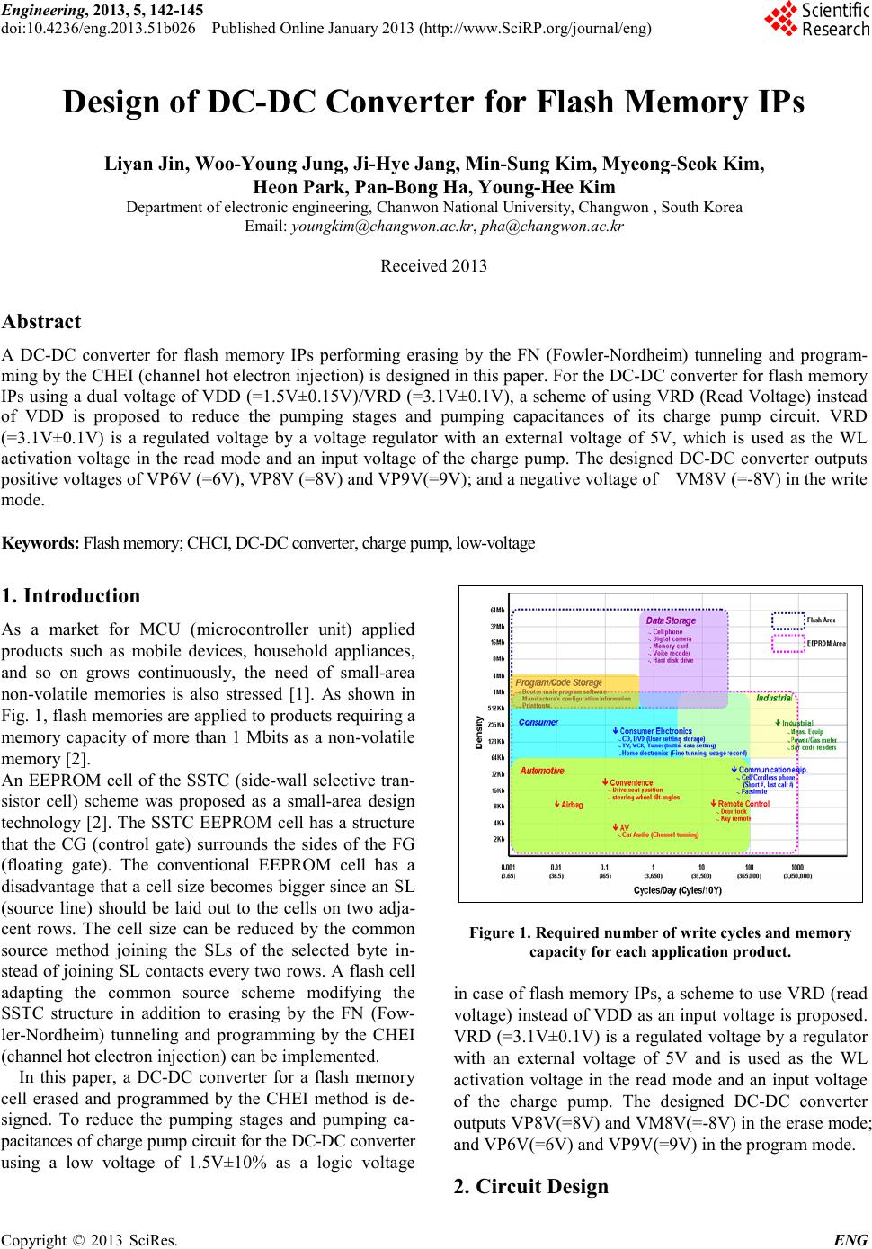 Engineering, 2013, 5, 142-145 doi:10.4236/eng.2013.51b026 Published Online January 2013 (http://www.SciRP.org/journal/eng) Copyright © 2013 SciRes. ENG Design of DC-DC Converter for F lash Memory IPs Liyan Jin, Woo-Young Jung, Ji-Hye Jang, Min-Sung Kim, Myeong-Seok Kim, Heon Park, Pan-Bong Ha, Young-Hee Kim Department of electron ic engin eer ing, Chanwon National University, Changwon , South Korea Email: youngkim@changwon.ac.kr, pha@changwon.ac.kr Received 2013 Abstract A DC-DC converter for flash memory IPs performing erasing by the FN (Fowler-Nordheim) tunneling and program- ming by the CHEI (cha n nel hot e lectro n injectio n) is desig ned in this paper . For the D C-D C converter for flash memory IPs using a dual voltage of VDD (=1.5V±0.15V)/VRD (=3.1V±0.1V), a scheme of using VRD (Read Voltage) instead of VDD is proposed to reduce the pumping stages and pumping capacitances of its charge pump circuit. VRD (=3.1V±0.1V) is a regulated voltage by a voltage regulator with an external voltage of 5V, which is used as the WL activation voltage in the read mode and an input voltage of the charge pump. The designed DC-DC converter outputs positive volta ges of VP6V (=6V), VP8V (=8V) and VP9V( =9V); and a negative voltage of VM8V (=-8V) in the write mode. Keywords: Flash memory; CHCI, DC-DC converter, charge pump, low-voltage 1. Introduction As a market for MCU (microcontroller unit) applied products such as mobile devices, household appliances, and so on grows continuously, the need of small-area non-volatile memories is also stressed [1]. As shown in Fig. 1, flash memorie s are ap plied to products req uiring a memory capacity of more than 1 Mbits as a non-volatile memory [2]. An EEPROM cell of the SSTC (side-wall selective tran- sistor cell) scheme was proposed as a small-area design technology [2]. The SSTC EEPROM cell has a structure that the CG (control gate) surrounds the sides of the FG (floating gate). The conventional EEPROM cell has a disadvantage that a cell size becomes bigger since an SL (source line) should be laid out to the cells on two adja- cent rows. The cell size can be reduced by the common source method joining the SLs of the selected byte in- stead of jo ining SL contac ts every two ro ws. A flash cell adapting the common source scheme modifying the SSTC structure in addition to erasing by the FN (Fow- ler-Nordheim) tunneling and programming by the CHEI (channel hot electron injection) can be i mplemented. In this paper, a DC-DC converter for a flash memory cell erased and programmed by the CHEI method is de- signed. To reduce the pumping stages and pumping ca- pacitanc es of charge pump circ uit for the DC-DC converter using a low voltage of 1.5V±10% as a logic voltage Figure 1 . Required number of write cy cles and memory capac ity for each appl ic ation produc t. in case o f flash memory IP s, a scheme to use VRD (read voltage) instead of VDD as an input voltage is proposed. VRD (=3.1V±0.1 V) is a regulated voltage by a regulator with an external voltage of 5V and is used as the WL activation voltage in the read mode a nd an input voltage of the charge pump. The designed DC-DC converter outputs VP8V(=8V) and VM8V(=-8V) in the erase mode; and VP6V(=6V) and VP9V(=9V) in the program mode. 2. Circuit Design 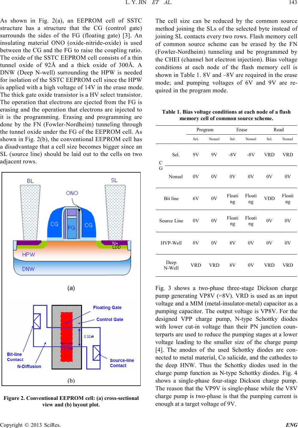 L. Y. JIN ET AL. Copyright © 2013 SciRes. ENG 143 As shown in Fig. 2(a), an EEPROM cell of SSTC structure has a structure that the CG (control gate) surrounds the sides of the FG (floating gate) [3]. An insulating material ONO (oxide-n itride-oxide) is used between the CG and the FG to r aise the couplin g ratio. The oxide of the SSTC EEPROM cell consists of a thin tunnel oxide of 92Å and a thick oxide of 300Å. A DNW (Deep N-well) surrounding the HPW is needed for isola tion o f the S ST C EE P ROM ce ll si nce t he HPW is applied with a high voltage of 14V in the erase mode. The thic k ga te o xide tr a ns istor is a H V se lec t tra n sisto r. The operation that electro ns are ejected from the FG is erasing and the operation that electrons are injected to it is the programming. Erasing and programming are done by the FN (Fowler-Nordheim) tunneling through the tunnel oxide under the FG of the EEPROM cell. As sho wn in F ig. 2 (b), the co nve ntio nal E EP ROM ce ll ha s a disadvanta ge that a c ell siz e becomes bigger si nce an SL (source line) should be laid out to the cells on two adjacent ro ws. Figure 2. Conventional EEPROM cell: (a) cross-sectional view and (b) la yo ut plot. The cell size can be reduced by the common source method joining the SLs of the selected byte instead of jo inin g S L co nt act s e ver y t w o ro ws. Fl as h memo ry c el l of common source scheme can be erased by the FN (Fowler -Nordheim) tunneling and be programmed by the CHEI (chan nel hot e lectro n injectio n). Bia s volta ge conditions at each node of the flash memory cell is sho wn i n T abl e 1. 8V a nd –8V are required in the era se mode; and pumping voltages of 6V and 9V are re- quired in the program mode. Table 1. Bias voltage c ondition s at each node of a flash memory cell of common source scheme. Program Erase R ead Se l. No nsel Se l. Nonsel Sel. Nonsel C G Sel. 9V 9V -8V -8V VRD VRD Nonsel 0V 0V 0V 0V 0V 0V Bit line 6V 0V Floati ng Floati ng VDD Floati ng Source Line 0V 0V Floati ng Floati ng 0V 0V HVP-Well 0V 0V 8V 0V 0V 0V Deep N-Well VRD VRD 8V 0V VRD VRD Fig. 3 shows a two-phase three-stage Dickson charge pump generating VP8V (=8V). VRD is used as an input voltage and a MIM (metal-insulator-metal) capacitor as a pumping capacitor. The output voltage is VP8V. For the designed VPP charge pump, N-type Schottky diodes with lower cut-in voltage than their PN junction coun- terparts are used to reduce the pumping stages at a lower voltage leading to the smaller size of the charge pump [4]. The anodes of the used Schottky diodes are con- nected to metal material, Co salicide, and the cathodes to the deep HNW. Thus the Schottky diodes used in the charge pump function as N-type Schottky diodes. Fig. 4 shows a single-phase four-stage Dickson charge pump. The reaso n that t he VP9 V is si ngle-phase while the V8V charge pump is two-phase is that the pumping current is enough at a target voltage of 9V. (a) (b) 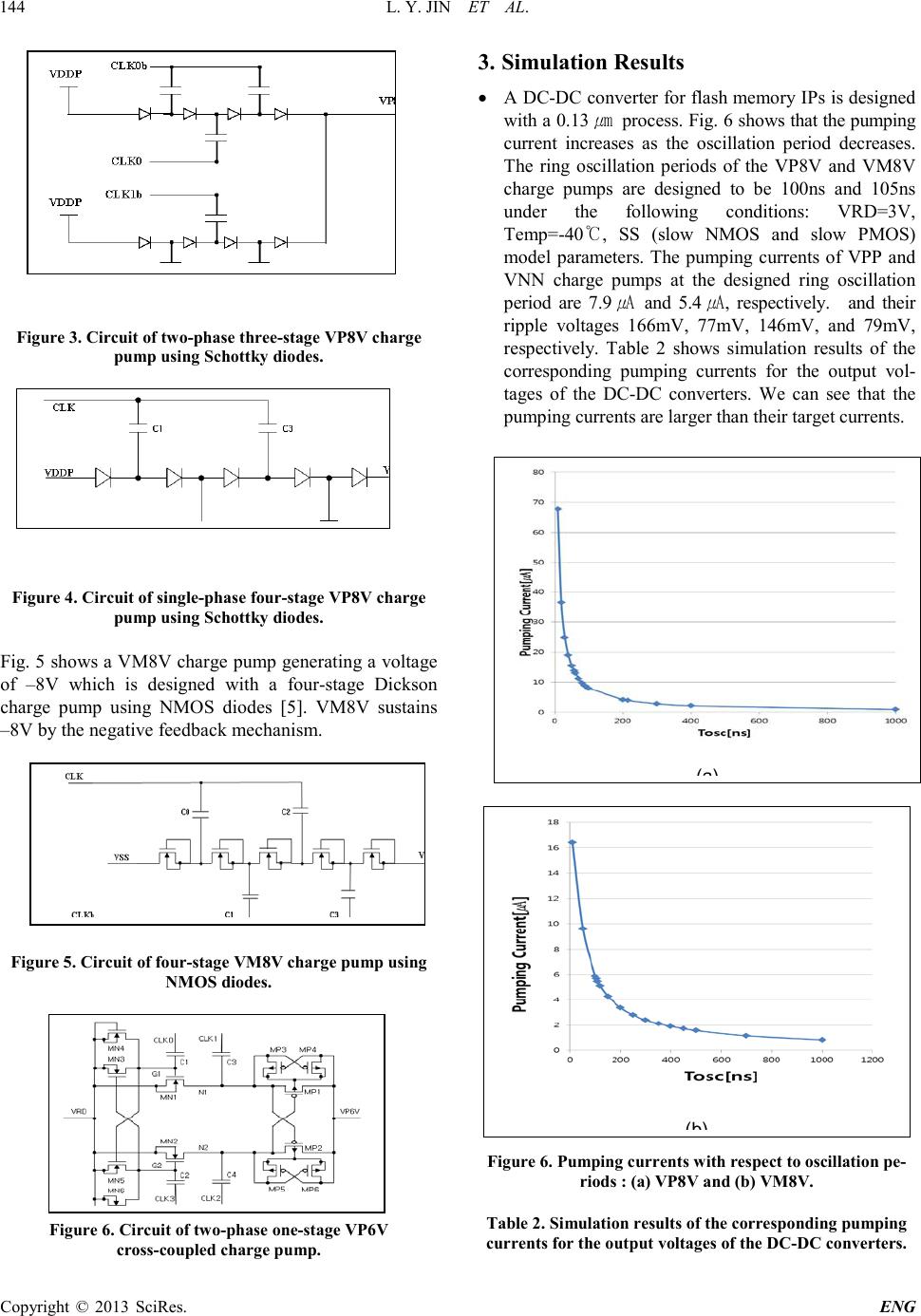 L. Y. JIN ET AL. Copyright © 2013 SciRes. ENG 144 Figure 3. Circuit of tw o-phase three-stage VP8V charge pump using Schot t ky di o des . Figure 4. Circuit of single-phase four-stage VP8 V c harge pump using Schot t ky di o des. Fig. 5 sho ws a V M8V cha rge pump genera ting a volta ge of –8V which is designed with a four-stage Dickson charge pump using NMOS diodes [5]. VM8V sustains –8V by the negative feedback mechanism. Figure 5. Circuit of four-stage VM8V charge p ump usi ng NMOS diodes. Figure 6. Circuit of tw o-ph as e o ne-stage VP6V cross-coupled charge pump. 3. Simulation Results • A DC-D C co nver ter for f las h me mor y IPs is de sig ned with a 0.13㎛ proce ss. Fig. 6 shows that the pumping current increases as the oscillation period decreases. The ring oscillation periods of the VP8V and VM8V charge pumps are designed to be 100ns and 105ns under the following conditions: VRD=3V, Temp=-40℃, SS (slow NMOS and slow PMOS) model parameters. The pumping currents of VPP and VNN charge pumps at the designed ring oscillation period are 7.9㎂ and 5.4㎂, respectively. and their ripple voltages 166mV, 77mV, 146mV, and 79mV, re spect ively. Table 2 shows simulation results of the corresponding pumping currents for the output vol- tages of the DC-DC converters. We can see that the pumping currents are larger than their target currents. Figure 6. Pumping currents wi th r e spect to oscillation pe- riods : (a) VP8V and (b) VM8V. Table 2. Simulation results of the co r res ponding pumping curr ents for the out put voltages of the DC-DC converters. (a) (b) 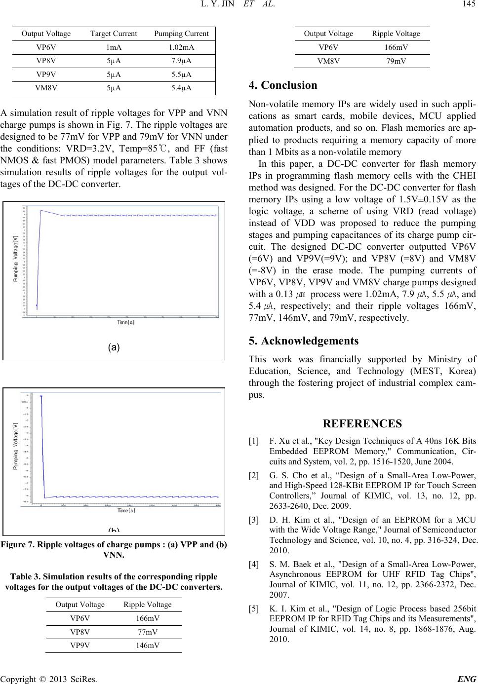 L. Y. JIN ET AL. Copyright © 2013 SciRes. ENG 145 Output Voltage Target Current Pumping Current VP6V 1mA 1.02mA VP8V 5µA 7.9µA VP9V 5µA 5.5µA VM8V 5µA 5.4µA A simulation result of ripple voltages for VPP and VNN char ge pump s is s hown in F ig. 7. The ripp le volta ges are designed to be 77mV for VPP and 79mV for VNN under the conditions: VRD=3.2V, Temp=85℃, and FF (fast NMOS & fast PMOS) model parameters. Table 3 shows simulation results of ripple voltages for the output vol- tages of the DC-DC converter. Figure 7. Ripple voltages of charge pumps : (a) VPP and (b) VNN. Table 3. Simulation results of the co r res ponding ripple voltag e s for the output voltages of the DC-DC converte rs . Output Voltage Ripple Voltage VP6V 166mV VP8V 77mV VP9V 146mV Output Voltage Ripple Voltage VP6V 166mV VM8V 79mV 4. Conclusion Non-volatile memory IPs are widely used in such appli- cations as smart cards, mobile devices, MCU applied automation products, and so on. Flash memories are ap- plied to products requiring a memory capacity of more than 1 Mbits a s a non-volatile memor y In this paper, a DC-DC converter for flash memory IPs in programming flash memory cells with the CHEI method was designed. For the DC-DC converter for flash memory IPs using a low voltage of 1.5V±0.15V as the logic voltage, a scheme of using VRD (read voltage) instead of VDD was proposed to reduce the pumping stages and pumping capacitances of its charge pump cir- cuit. The designed DC-DC converter outputted VP6V (=6V) and VP9V(=9V); and VP8V (=8V) and VM8V (=-8V) in the erase mode. The pumping currents of VP6V, VP8 V, VP9V and VM 8V charge pumps desig ned with a 0.13㎛ process were 1.02mA, 7.9㎂, 5.5㎂, and 5.4 ㎂, respectively; and their ripple voltages 166mV, 77mV, 146mV, and 79mV, respectively. 5. Acknowledgements This work was financially supported by Ministry of Education, Science, and Technology (MEST, Korea) through the fostering project of industrial complex cam- pus. REFERENCES [1] F. Xu et al., "Key Design Techniques of A 40ns 16K Bits Embedded EEPROM Memory," Communication, Cir- cuits and System, vol. 2, pp. 1516-15 20, June 20 04. [2] G. S. Cho et al., “Design of a Small-Area Low-Power, and High-Speed 128-KBit EEP ROM IP for To uch Scr een Controllers,” Journal of KIMIC, vol. 13, no. 12, pp. 2633-2640, Dec. 20 09. [3] D. H. Kim et al., "Design of an EEPROM for a MCU with the Wide Voltage Range," Journal of Semiconductor Technology and Science, vol. 10, no. 4, pp. 316-324, Dec. 2010. [4] S. M. Baek et al., "Design of a Small-Area Low-Power, Asynchronous EEPROM for UHF RFID Tag Chips", Journal of KIMIC, vol. 11, no. 12, pp. 2366-2372, Dec. 2007. [5] K. I. Kim et al., "Design of Logic Process based 256bit EEPROM IP for RFID Tag Chips and its Measurements", Journal of KIMIC, vol. 14, no. 8, pp. 1868-1876, Aug. 2010. (a) (b) |