Paper Menu >>
Journal Menu >>
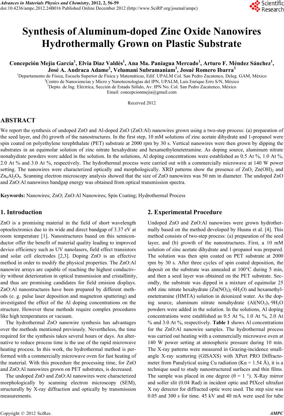 Advances in Materials Physics and Chemistry, 2012, 2, 56-59 doi:10.4236/ampc.2012.24B016 Published Online December 2012 (http://www.SciRP.org/journal/ampc) Synthesis of Aluminum-doped Zinc Oxide Nanowires Hydrothermally Grown on Plastic Substrate Concepción Mejía García1, Elvia Díaz Valdés1, Ana Ma. Paniagua Mercado1, Arturo F. Méndez Sánchez1, José A . Andr aca Adame2, Velumani Subr amaniam3, Josué Romero Ibarra3 1Departamento de Física, Escuela Superior de Física y Matemáticas, Edif. UPALM Col. San Pedro Zacatenco, Deleg. GAM, México 2Centro de Nanociencias y Micro y Nanotecnologías del IPN, UPALM, Luis Enrique Erro S/N, México 3Depto. de Ing. Eléctrica, Sección de Estado Sólido, Av. IPN No. Col. San Pedro Zacatenco, México Email: concepcionmejia@gmail.com Received 2012 ABSTRACT We report the synthesis of undoped ZnO and Al-doped ZnO (ZnO:Al) nanowires grown using a two-step process: (a) preparation of the seed layer, and (b) growth of the nanostructures. In the first step, 10 mM solutions of zinc acetate dihydrate and 1-propanol were spin coated on polyethylene terephthalate (PET) substrate at 2000 rpm by 30 s. Vertical nanowires were then grown by dipping the substrates in an equimolar solution of zinc nitrate hexahydrate and hexamethylenetetramine. As doping source, aluminum nitrate nonahydrate powders were added in the solution. In the solutions, Al doping concentrations were established as 0.5 At %, 1.0 At %, 2.0 At % and 3.0 At %, respectively. The hydrothermal process were carried out with a commercially microwave at 140 W power setting. The nanowires were characterized optically and morphologically. XRD patterns show the presence of ZnO, Zn(OH)2 and Zn6Al2O9. Scanning electron microscopy analysis showed that the size of ZnO nanowires was 50 nm in diameter. The undoped ZnO and ZnO:Al nanowires bandgap energy was obtained from optical transmission spectra. Keywords: Nanowires; ZnO; ZnO:Al Nanowires; Spin Coating; Hydrothermal Process 1. Introduction ZnO is a promising material in the field of short wavelength optoelectronics due to its wide and direct bandgap of 3.37 eV at room temperature [1]. Nanostructures based on this semicon- ductor offer the benefit of material quality leading to improved device efficiency such as UV nanolasers, field effect transistors and solar cell electrodes [2,3]. Doping ZnO is an effective method in order to modify the physical properties. The ZnO:Al nanowire arrays are capable of reaching the highest conductiv- ity without deterioration in optical transmission and cristallinity, and thus are promising candidates for field emision displays. ZnO:Al nanostructures have been prepared by different meth- ods (e. g. pulse laser deposition and magnetron sputtering) and investigated the effect of the Al doping concentrations on the structure. However these methods require complex procedures like high temperatures or vacuum. The hydrothermal ZnO nanowire synthesis has advantages over the methods mentioned previously. Nevertheless, the time required for the synthesis takes several hours or days. An alter- native to reduce process time is the use of the rapid microwave heating process. In this work, the hydrothermal method is per- formed with a commercially microwave oven for fast heating of the material. With this procedure the processing time, for ZnO and ZnO:Al nanowires grown on PET substrates, is decreased. The undoped ZnO and ZnO:Al nanowires were characterized morphologically by scanning electron microscopy (SEM), structurally by X-ray diffraction and optically by transmission measurements. 2. Experimental Procedure Undoped ZnO and ZnO:Al nanowires were grown hydrother- mally based on the method developed by Husnu et al. [4]. This method consists of two-step process: (a) preparation of the seed layer, and (b) growth of the nanostructures. First, a 10 mM solution of zinc acetate dihydrate and 1-propanol was prepared. The solution was then spin coated on PET substrate at 2000 rpm by 30 s. After three cycles of spin coated deposition, the deposit on the substrate was annealed at 100°C during 5 min, and then a seed layer was obtained on the PET substrate. Sec- ondly, the substrate was dipped in a mixture of equimolar 25 mM zinc nitrate hexahydrate (Zn(NO3)2·6H2O) and hexamethyl- enetetramine (HMTA) solution in deionized water. As the dop- ing source, aluminum nitrate nonahydrate (Al(NO3)3·9H2O powders were added in the solution. In the solutions, Al doping concentrations were established as 0.5 At %, 1.0 At %, 2.0 At % and 3.0 At %, respectively. Table 1 shows Al concentrations for the ZnO:Al nanowire samples. The hydrothermal process was carried out heating with a commercially microwave oven at 140 W power setting at atmospheric pressure during 10 min. The X-ray patterns were measured in Grazing-incidence small- angle X-ray scattering (GISAXS) with XPert PRO Diffracto- meter from Panalytical using Cu radiation (Kα = 1.54 Å), it is a technique used to study nanostructured surfaces and thin films. The sample was placed in one degree (θ = 1 °). X-Ray mirror and soller slit (0.04 Rad) in incident optic and PIXcel ultrafast X ray detector for diffracted optic were used. The step size was 0.05 and 300 s for time. 45 kV and 40 mA were used for tube Copyright © 2012 SciRes. AMPC 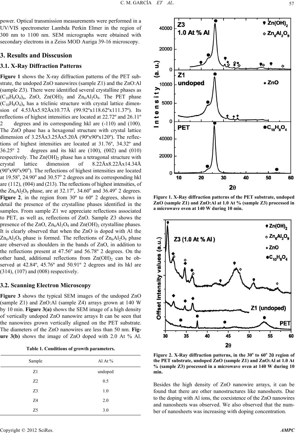 C. M. GARCÍA ET AL. 57 power. Optical transmission measurements were performed in a UV/VIS spectrometer Lambda Perkin Elmer in the region of 300 nm to 1100 nm. SEM micrographs were obtained with secondary electrons in a Zeiss MOD Auriga 39-16 microscopy. 3. Results and Disscusion 3.1. X-Ray Diffraction Patterns Figure 1 shows the X-ray diffraction patterns of the PET sub- strate, the undoped ZnO nanowires (sample Z1) and the ZnO:Al (sample Z3). There were identified several crystalline phases as (C10H8O4)n, ZnO, Zn(OH)2 and Zn6Al2O9. The PET phase (C10H8O4)n has a triclinic structure with crystal lattice dimen- sion of 4.53Åx5.92Åx10.77Å (99.92ºx118.62ºx111.37º). Its reflections of highest intensities are located at 22.72º and 26.11º 2degrees and its corresponding hkl are ( -110) and (100). The ZnO phase has a hexagonal structure with crystal lattice dimension of 3.25Åx3.25Åx5.20Å (90ºx90ºx120º). The reflec- tions of highest intensities are located at 31.76º, 34.32º and 36.25º 2degrees and its hkl are (100), (002) and (010) respectively. The Zn(OH)2 phase has a tetragonal structure with crystal lattice dimension of 8.22Åx8.22Åx14.34Å (90ox90ox90o). The reflections of highest intensities are located at 19.58o, 24.90o and 30.57o 2 degrees and its corresponding hkl are (112), (004) and (213). The reflections of highest intensities, of the Zn6Al2O9 phase, are at 32.17o, 34.60o and 36.49o 2 degrees. Figure 2, in the region from 30º to 60º 2 degrees, shows in detail the presence of the crystalline phases identified in the samples. From sample Z1 we appreciate reflections associated to PET, as well as, reflections of ZnO. Sample Z3 shows the presence of the ZnO, Zn6Al2O9 and Zn(OH)2 crystalline phases. It is clearly observed that when the ZnO is doped with Al the Zn6Al2O9 phase is formed. The reflections of Zn6Al2O9 phase are observed as shoulders in the bands of ZnO, in addition to the reflections present at 47.56º and 56.78º 2 degrees. On the other hand, additional reflections from Zn(OH)2 can be ob- served at 42.84º, 45.76º and 50.91º 2 degrees and its hkl are (314), (107) and (008) respectively. 3.2. Scanning Electron Microscopy Figure 3 shows the typical SEM images of the undoped ZnO (sample Z1) and ZnO:Al (sample Z4) arrays grown at 140 W by 10 min. Figure 3(a) shows the SEM image of a high density of vertically undoped ZnO nanowire arrays It can be seen that the nanowires grown vertically aligned on the PET substrate. The diameters of the ZnO nanowires are less than 50 nm. Fig- ure 3(b) shows the image of ZnO doped with 2.0 At % Al. Table 1. Conditions of growth parameters. Sample Al At % Z1 undoped Z2 0.5 Z3 1.0 Z4 2.0 Z5 3.0 Figure 1. X-Ray diffraction patterns of the PET substrate, undoped ZnO (sample Z1) and ZnO:Al at 1.0 At % (sample Z3) processed in a microwave oven at 140 W during 10 min. Figure 2. X-Ray diffraction patterns, in the 30o to 60o 2 region of the PET substrate, undoped ZnO (sample Z1) and ZnO:Al at 1.0 At % (sample Z3) processed in a microwave oven at 140 W during 10 min. Besides the high density of ZnO nanowire arrays, it can be found that there are other nanostructures like nanosheets. Due to the doping with Al ions, the coexistence of the ZnO nanowires and nanosheets was observed. We also observed that the num- ber of nanosheets was increasing with doping concentration. Copyright © 2012 SciRes. AMPC 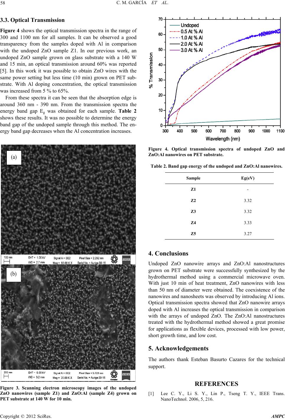 C. M. GARCÍA ET AL. 58 3.3. Optic al Tr ansmission Figure 4 shows the optical transmission spectra in the range of 300 and 1100 nm for all samples. It can be observed a good transparency from the samples doped with Al in comparison with the undoped ZnO sample Z1. In our previous work, an undoped ZnO sample grown on glass substrate with a 140 W and 15 min, an optical transmission around 60% was reported [5]. In this work it was possible to obtain ZnO wires with the same power setting but less time (10 min) grown on PET sub- strate. With Al doping concentration, the optical transmission was increased from 5 % to 65%. From these spectra it can be seen that the absorption edge is around 360 nm - 390 nm. From the transmission spectra the energy band gap Eg was obtained for each sample. Table 2 shows these results. It was no possible to determine the energy band gap of the undoped sample through this method. The en- ergy band gap decreases when the Al concentration increases. (a) (b) Figure 3. Scanning electron microscopy images of the undoped ZnO nanowires (sample Z1) and ZnO:Al (sample Z4) grown on PET substrate at 140 W for 10 min. Figure 4. Optical transmission spectra of undoped ZnO and ZnO:Al nanowires on PET substrate. Table 2. Band gap energy of the undoped and ZnO:Al nanowires. Sample Eg(eV) Z1 - Z2 3.32 Z3 3.32 Z4 3.33 Z5 3.27 4. Conclusions Undoped ZnO nanowire arrays and ZnO:Al nanostructures grown on PET substrate were successfully synthesized by the hydrothermal method using a commercial microwave oven. With just 10 min of heat treatment, ZnO nanowires with less than 50 nm of diameter were obtained. The coexistence of the nanowires and nanosheets was observed by introducing Al ions. Optical transmission spectra showed that ZnO nanowire arrays doped with Al increases the optical transmission in comparison with the arrays of undoped ZnO. The ZnO:Al nanostructures treated with the hydrothermal method showed a great promise for applications as flexible devices, processed with low power, short growth time, and low cost. 5. Acknowledgements The authors thank Esteban Basurto Cazares for the technical support. REFERENCES [1] Lee C. Y., Li S. Y., Lin P., Tseng T. Y., IEEE Trans. NanoTechnol. 2006, 5, 216. Copyright © 2012 SciRes. AMPC 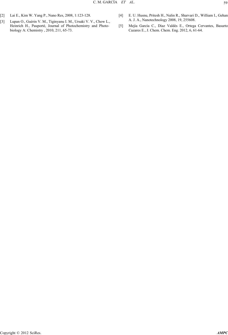 C. M. GARCÍA ET AL. Copyright © 2012 SciRes. AMPC 59 [2] Lai E., Kim W. Yang P., Nano Res, 2008, 1:123-128. [3] Lupan O., Guérin V. M., Tiginyanu I. M., Ursaki V. V., Chow L., Heinrich H., Pauporté, Journal of Photochemistry and Photo- biology A: Chemistry , 2010, 211, 65-73. [4] E. U. Husnu, Pritesh H., Nalin R., Sharvari D., William I., Gehan A. J. A., Nanotechnology 2008, 19, 255608. [5] Mejía García C., Díaz Valdés E., Ortega Cervantes, Basurto Cazares E., J. Chem. Chem. Eng. 2012, 6, 61-64. |