R. AMRANI ET AL.
60
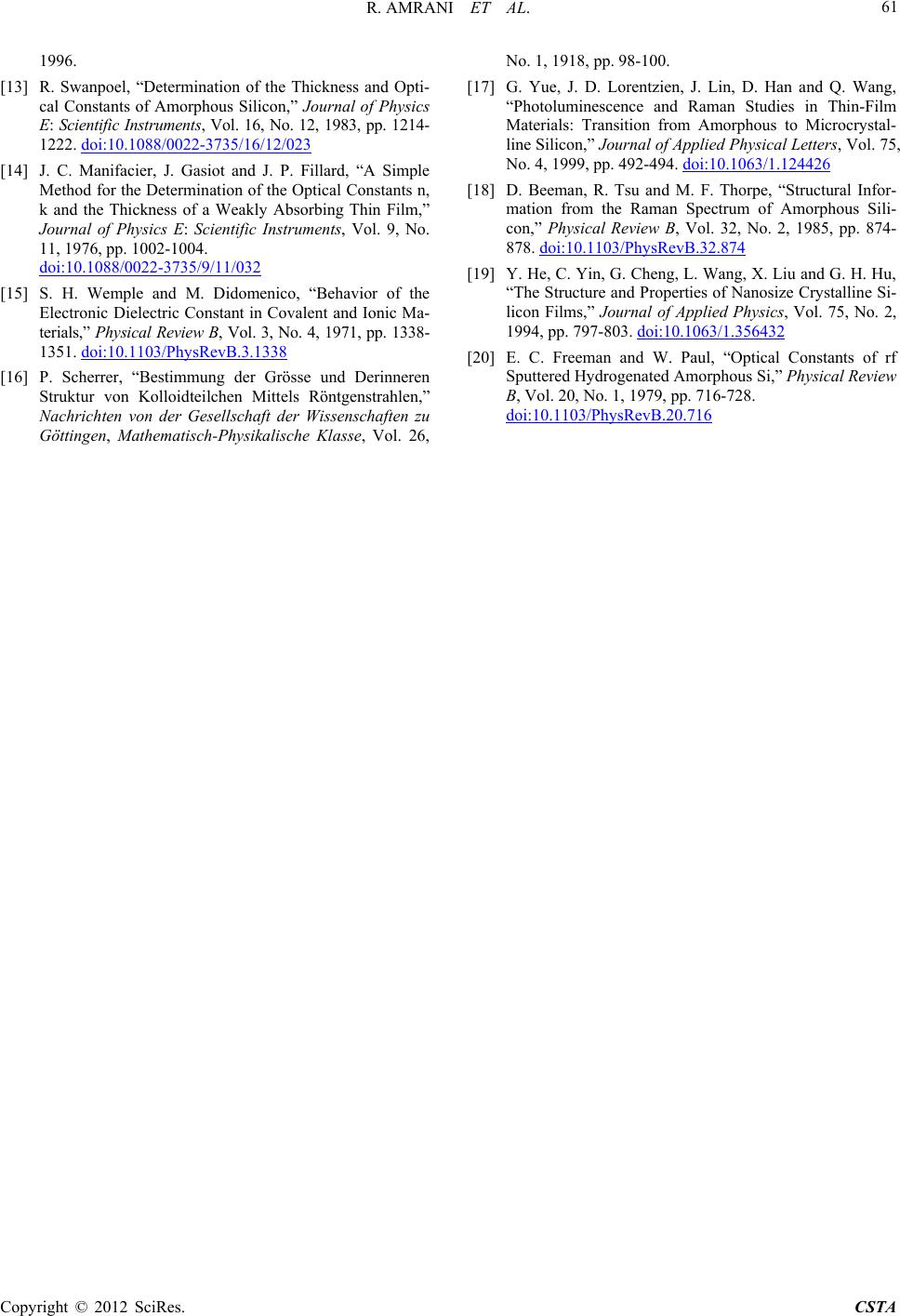
200 W and beyond 800 mTorr, EM decreases considera-
bly. This confirms once again, that beyond these deposi-
tion parameters, an amorphous-nanocrystalline transition
is observed.
The RF bias voltage is an important deposition pa-
rameter of nc-Si:H films. During the growth, the RF bias
has a decisive effect on the energy and natures of (SiHn)
species [19]. The appropriate bias may control the reac-
tion rate at the gas-substrate interface, so as to promote
the nucleation rate, and enhance the densification of
nanocrystallites in the growing films. He et al. demon-
strate also, that bias voltage controls the crystalline frac-
tion for nc-Si:H samples [19]. In this work, and at certain
deposition parameters, the bias varies. For power more
than 200 W and pressure below 800 mTorr, RF bias in-
creases from 3 V to 80 V, after a few minutes for the
beginning of the deposition process. The reflect RF
power is also an important parameter. After a specific
deposition time (~10 min), the reflect power increases,
and in consequence the real power deposition decreases.
To resolve the effects of RF bias and RF power reflect
values, samples were deposited with layer by layer (LBL)
deposition method.
4. Conclusion
As conclusion, we have proved that the formation of
powders in Silane-Argon plasma, initially considered as
a drawback, can be exploited to produce nanocrystalline
silicon particles. We have shown that hydrogenated
nanocrystalline silicon (nc-Si:H) films can be prepared
from silane argon mixture without hydrogen dilution at
high deposition rates (~10 Å/s) and at low substrate tem-
perature (200˚C) using PECVD method. The structural
evolution studies show that beyond 200 W RF power and
beyond 800 mTorr pressure deposition conditions, we
observed an amorphous-nanocrystalline transition. From
the present study it has been concluded that the process
pressure and RF power are the key process parameters to
induce the crystallinity in the Si:H films grown by
PECVD method. From materials and devices application,
especially, photovoltaic devices application, nanocrystal-
line silicon produced at low temperature in silane plasma,
open the way to new applications, like the deposition on
flexible substrate.
5. Acknowledgements
The authors would like to thank D. Bourgogne for Ra-
man experiments assistance and B. Fraisse for the X-ray
diffraction measurements. This work is kindly supported
by Averroes Program.
REFERENCES
[1] W. E. Spear and P. G. LeComber, “Subtitutional Doping
of Amorphous Silicon,” Solid State Communications, Vol.
17, No. 9, 1975, pp. 1193-1196.
doi:10.1016/0038-1098(75)90284-7
[2] D. L. Staebler and C. R. Wronki, “Reversible Conduc-
tivity Changes in Discharge Produced Amorphous Si,”
Applied Physical Letters, Vol. 31, No. 4, 1977, p. 292.
doi:10.1063/1.89674
[3] H. Li, R. H. Franken, R. L. Stolk, C. H. M. van der Werf,
J. K. Rath and R. E. I. Schropp, “Controlling the Quality
of Nanocrystalline Silicon Made by Hot-Wire Chemical
Vapor Deposition by Using a Reverse H2 Profiling Tech-
nique,” Journal of Non-Crystalline Solids, Vol. 354, No.
19-25, 2008, pp. 2087-2091.
[4] M. Birkholz, B. Selle, E. Conrad, K. Lips and W. Fuhs,
“Evolution of Structure in Thin Microcrystalline Silicon
Films Grown by Electron-Cyclotron Resonance Chemical
Vapor Deposition,” Journal of Applied Physics, Vol. 88,
No. 7, 2000, pp. 4376-4379. doi:10.1063/1.1289783
[5] B. Rech, T. Roschek, J. Müller, S. Wieder and H. Wagner,
“Amorphous and Microcrystalline Silicon Solar Cells
Prepared at High Deposition Rates Using RF (13.56 MHz)
Plasma Excitation Frequencies,” Solar Energy Materials
and Solar Cells, Vol. 66, No. 1-4, 2001, pp. 267-273.
doi:10.1016/S0927-0248(00)00183-5
[6] Y. Mai, S. Klein, R. Carius, L. Houben, X. Geng and F.
Finger, “Improvement of Open Circuit Voltage in Micro-
crystalline Silicon Solar Cells Using Hot Wire Buffer
Layers,” Journal of Non-Crystalline Solids, Vol. 352, No.
9-20, 2006, pp. 1859-1862.
[7] M. van Veen, C. van der Werf and R. Schropp, “Tandem
Solar Cells Deposited Using Hot-Wire Chemical Vapor
Deposition,” Journal of Non-Crystalline Solids, Vol. 338-
340, No. 1, 2004, pp. 655-658.
doi:10.1016/j.jnoncrysol.2004.03.071
[8] R. Amrani, D. Benlekehal, R. Baghdad, D. Senouci, A.
Zeinert, K. Zellama, L. Chahed, J. D. Sib and Y. Bouizem,
“Low-Temperature Growth of Nanocrystalline Silicon
Films Prepared by RF Magnetron Sputtering: Structural
and Optical Studies,” Journal of Non-Crystalline Solids,
Vol. 354, No. 19-25, 2008, pp. 2291-2295.
doi:10.1016/j.jnoncrysol.2007.10.044
[9] J. L. Dorier, C. Hollenstein, A. A. Howling and U. Kroll,
“Powder Dynamics in Very High Frequency Silane Plas-
mas,” Journal of Vacuum Science & Technology, Vol.
A10, No. 4, 1992, pp. 1048-1052. doi:10.1116/1.578200
[10] J. L. Dorier, C. Hollenstein and A. A. Howling, “Spatio-
temporal Powder Formation and Trapping in Radio Fre-
quency Silane Plasmas Using Two-Dimensional Polari-
zation-Sensitive Laser Scattering,” Journal of Vacuum
Science & Technology, Vol. A13, No. 3, 1995, pp. 918-
926. doi:10.1116/1.579852
[11] A. A. Howling, J. L. Dorier, C. Hollenstein, U. Kroll and
F. Finger, “Frequency Effects in Silane Plasmas for
Plasma Enhanced Chemical Vapor Deposition,” Journal
of Vacuum Science & Technology, A10, No. 4, 1992, pp.
1080-1085. doi:10.1116/1.578205
[12] J. L. Dorier,“Genèse, Croissance et Conséquences de
Particules Dans les Plasmas en Silane à Basse Pression et
Basse Température,” Ph.D. Thesis, E.P.F.L, Switzerland,
Copyright © 2012 SciRes. CSTA