 Optics and Photonics Journal, 2012, 2, 326-331 http://dx.doi.org/10.4236/opj.2012.24040 Published Online December 2012 (http://www.SciRP.org/journal/opj) The Efficiency of a p-n Solar Diode as a Function of the Recombination Velocity within the Depletion Layer Mohamed K. El-Adawi1, Najla S. Al-Shameri2 1Physics Department, Faculty of Education, Ain Shams University, Cairo, Egypt 2Physics Department, College of Science for Girls, Dammam University, Dammam, KSA Email: adawish1@hotmail.com Received September 14, 2012; revised October 16, 2012; accepted October 30, 2012 ABSTRACT The role of the carrier’s recombination velocity i within the depletion Layer of junction solar cell and the ex- ternal bias voltage across the junction in determining the current density “J” through the cell is revealed. The un- steady carrier diffusion equation is solved under illumination conditions considering a source spectral function -pn a V G . The efficiency of the device as a function of i , , a V G is obtained. Computations considering a silicon solar cell are given as an illustrative example. Keywords: Efficiency; Diffusion Equation; Recombination Velocity 1. Introduction The performance of a solar cell has aroused the interest of many investigators [1-17]. The solar p-n cell is a semiconductor photovoltaic cell. It is a passive trans- ducer. It is fabricated such that one region is more highly doped denoted by region. The density of the charge carriers in the highly doped region may be of three orders larger than the other region. This surface is usually subjected to the incident illuminations (emitter region). Due to large gradients, diffusion of charge carri- ers take place, holes from or np P region diffuse to the n- region, while electrons diffuse from n-region to P region. As a result a depletion layer is formed on both sides of the contact metallurgical surface between both sides. This layer is of small thickness and is called as the space-charge region (SCR). This layer con- tains the positive ions of the donner atoms on one side of the contact surface and the negative ions of the acceptor atoms on the other side, and thus an electric field is built and one gets what is called the built-in-voltage 1μm bi . It is also called the contact potential or the barrier potential. The direction of the electric field within the depletion layer will be from the N-region to the P-region. V At equilibrium the net current (the sum of the diffusion currents and the drift currents) through the depletion layer must be zero. Now if the cell is subjected to an ex- ternal reverse voltage bias, the established external field will strengthen the internal one, and less current density passes through the depletion layer and vice versa [18]. This bias voltage disturbs the thermal equilibrium state of the device. When light strikes the highly doped sur- face, the absorbed quanta excite the bound electrons and electron-hole pairs are produced that move in all direc- tions within the crystal [2]. The electron-hole generation process is accompanied with recombination processes. Now if the bias voltage is switched off, the built- in-voltage will change towards its equilibrium value, through a recombination process between the electrons and the holes during the decay of the external voltage [3]. The equilibrium state will be restored within a time in- terval called as the relaxation time or it is defined as the minority carrier life time .It is worth to note that the electric potential across the depletion layer controls its electric resistance [4]. Different factors affect the charge transport properties within the cell, such as the electric potential across the device, the recombination velocity between the charge carriers. The most important factor is the doping level [5,6]. This factor can be controlled through the fabrication technology. These factors affect the current density passing through the cell and thus change its efficiency. Different trials are oriented to study the performance of the solar cell through the study of the recombination velocity between the charge carri- ers. With this respect one finds in principal two trends namely: C opyright © 2012 SciRes. OPJ 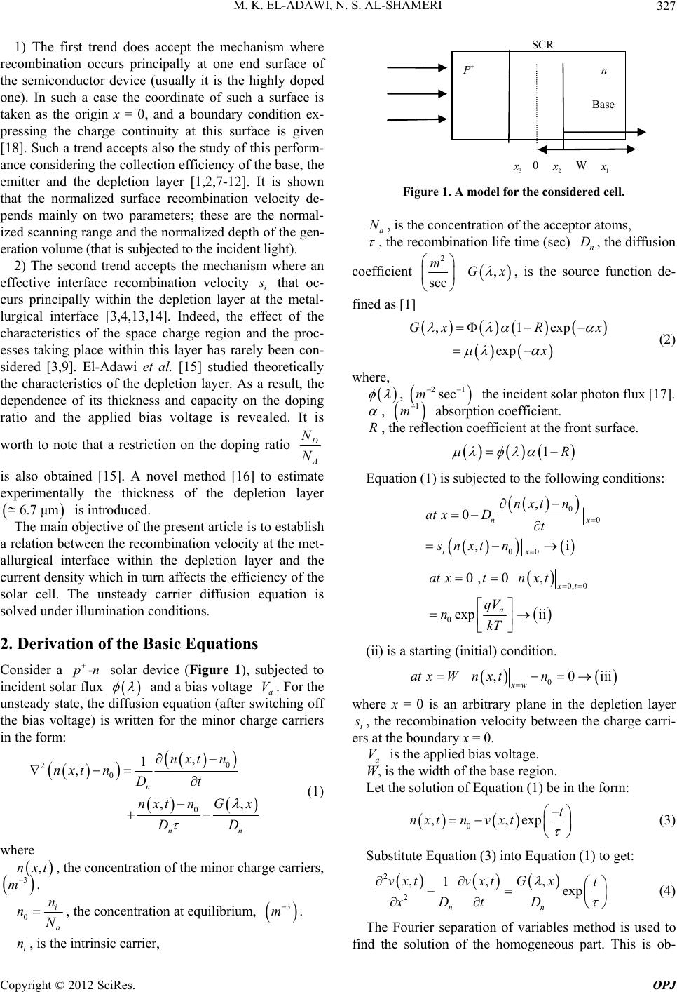 M. K. EL-ADAWI, N. S. AL-SHAMERI 327 1) The first trend does accept the mechanism where recombination occurs principally at one end surface of the semiconductor device (usually it is the highly doped one). In such a case the coordinate of such a surface is taken as the origin x = 0, and a boundary condition ex- pressing the charge continuity at this surface is given [18]. Such a trend accepts also the study of this perform- ance considering the collection efficiency of the base, the emitter and the depletion layer [1,2,7-12]. It is shown that the normalized surface recombination velocity de- pends mainly on two parameters; these are the normal- ized scanning range and the normalized depth of the gen- eration volume (that is subjected to the incident light). 2) The second trend accepts the mechanism where an effective interface recombination velocity i that oc- curs principally within the depletion layer at the metal- lurgical interface [3,4,13,14]. Indeed, the effect of the characteristics of the space charge region and the proc- esses taking place within this layer has rarely been con- sidered [3,9]. El-Adawi et al. [15] studied theoretically the characteristics of the depletion layer. As a result, the dependence of its thickness and capacity on the doping ratio and the applied bias voltage is revealed. It is worth to note that a restriction on the doping ratio A N N is also obtained [15]. A novel method [16] to estimate experimentally the thickness of the depletion layer is introduced. 6.7 μm The main objective of the present article is to establish a relation between the recombination velocity at the met- allurgical interface within the depletion layer and the current density which in turn affects the efficiency of the solar cell. The unsteady carrier diffusion equation is solved under illumination conditions. 2. Derivation of the Basic Equations Consider a solar device (Figure 1), subjected to incident solar flux -pn and a bias voltage a. For the unsteady state, the diffusion equation (after switching off the bias voltage) is written for the minor charge carriers in the form: V 0 2 0 0 , 1 , ,, n nn nxtn nxtnDt nxtnGx DD (1) where ,nxt 3 m, the concentration of the minor charge carriers, . 0 i a n nN , the concentration at equilibrium, 3 m. i n, is the intrinsic carrier, P + n Base SCR 3 0 2 W 1 Figure 1. A model for the considered cell. a N, is the concentration of the acceptor atoms, , the recombination life time (sec) , the diffusion n D coefficient 2 sec m ,Gx , is the source function de- fined as [1] ,1exp exp GxR x x (2) where, , 21 secm the incident solar photon flux [17]. , 1 m absorption coefficient. R, the reflection coefficient at the front surface. 1R Equation (1) is subjected to the following conditions: 0 0 00 , 0 ,i nx ix nxtn at xDt snxt n 0, 0 0 0 ,0, exp ii t a at xtnx t qV nkT (ii) is a starting (initial) condition. 0 ,0 iii xw at xWnx tn where x = 0 is an arbitrary plane in the depletion layer i , the recombination velocity between the charge carri- ers at the boundary x = 0. a W, is the width of the base region. V is the applied bias voltage. Let the solution of Equation (1) be in the form: 0 ,,exp t nxtnvxt (3) Substitute Equation (3) into Equation (1) to get: 2 2 ,,, 1exp nn vxtvxtG xt Dt D x (4) The Fourier separation of variables method is used to find the solution of the homogeneous part. This is ob- Copyright © 2012 SciRes. OPJ 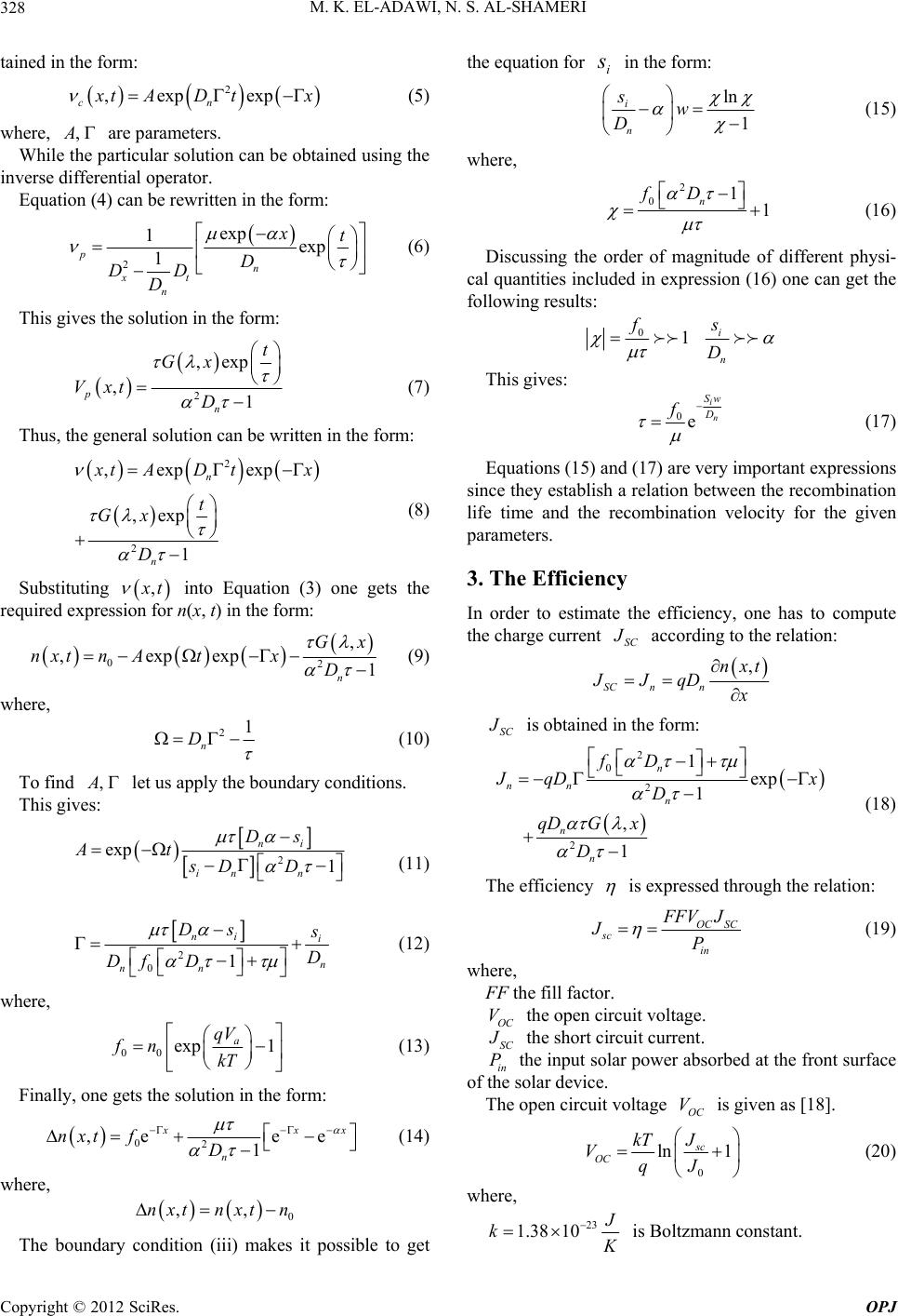 M. K. EL-ADAWI, N. S. AL-SHAMERI 328 tained in the form: 2 ,exp exp cn tA Dtx (5) where, , are parameters. While the particular solution can be obtained using the inverse differential operator. Equation (4) can be rewritten in the form: 2 exp 1exp 1 pn xt n xt D DD D (6) This gives the solution in the form: 2 ,exp ,1 p n t Gx Vxt D (7) Thus, the general solution can be written in the form: 2 2 ,exp exp ,exp 1 n n tA Dtx t Gx D (8) Substituting , t into Equation (3) one gets the required expression for n(x, t) in the form: 02 , ,expexp 1 n Gx nxtnAtxD (9) where, 21 n D (10) To find , let us apply the boundary conditions. This gives: 2 exp 1 ni in n Ds At sD D (11) 2 01 ni i n nn Ds D Df D (12) where, 00 exp 1 a qV fn kT (13) Finally, one gets the solution in the form: 02 ,e ee 1 xx n nxtfD (14) where, 0 ,,nxtnxtn The boundary condition (iii) makes it possible to get the equation for in the form: i s ln 1 i n sw D (15) where, 2 011 n fD (16) Discussing the order of magnitude of different physi- cal quantities included in expression (16) one can get the following results: 01 f i n s D This gives: 0e i n Sw f (17) Equations (15) and (17) are very important expressions since they establish a relation between the recombination life time and the recombination velocity for the given parameters. 3. The Efficiency In order to estimate the efficiency, one has to compute the charge current SC according to the relation: , SC nn nxt JJqD SC is obtained in the form: 2 0 2 2 1 exp 1 , 1 n nn n n n fD qD x D qD Gx D (18) The efficiency is expressed through the relation: OC SC sc in FV J JP (19) where, FF the fill factor. OC V the open circuit voltage. SC the short circuit current. in the input solar power absorbed at the front surface of the solar device. P The open circuit voltage is given as [18]. OC V 0 ln 1 sc OC J kT VqJ (20) where, 23 1.38 10 k is Boltzmann constant. Copyright © 2012 SciRes. OPJ  M. K. EL-ADAWI, N. S. AL-SHAMERI 329 0 ,TK is the absolute temperature. 02 , Jm is the diode saturation current density. 19 1.6 10Cq is the charge of an electron. The value of 0 is expressed as [19] 3 0exp g E JAT kT (21) where, A is the ideality factor. It is taken as unity for simplification. E is the energy gap expressed as [20]. 2 0 gg aT ET ETb (22) where, a and b are parameters. 4. Computations As an illustrative example, computations for a silicon p-n solar cell are given concerning the above mentioned functions. For a silicon solar cell [20]: 4 4.7310eV Ka , 0 636bK 01.17eV g E, 0 300TK The following values for further parameters are also considered [1,17,21]: 2 421 n 10 319 02 m 10.678, D32.310, 810m, sec 1 n110m, 710 msec R 1) The recombination life time as a function of the re- combination velocity is computed first with “W” as a parameter, then for a V as a parameter. The obtained results are illustrated graphically in Figures 2 and 3. It is clear that as the recombination velocity increases the recombination life time decreases. 2) The relation between ,nxt Volts, and “x” for follow- ing parameters: a V0.40 20msec i s ustrated graphically in Figure 4. It is clear that the function and 6 0.41 10sec , is ill ,nxt es with “x” through the cell. decreas 3) The current density “J” and the efficiency is computed. The following values of the applied voltage a are considered as parameters: 0.51, 0.52, 0.53, 0.54 volts. V The obtained values are given in Table 1 and are illus- trated graphically in Figure 5. 5. Conclusions The obtained results reveal that: 020 40 60 80100120140 0 0.5 1 1.5 x 10⁻⁶ recom b i n ation velocity (m /sec ) w=200e-6 w=400e-6 w=600e-6 (sec) Figure 2. A relation between the recombination life time and the recombination velocity for “W” as a parameter. 02040 6080100120140 0 1 2 3 4 5 6 7x 10⁻⁶ rec om bi nat i on veloc i t y (m/s ec) V a=0.40v V a=0.42v V a=0.44v (sec) W = 200 microns Figure 3. A relation between the recombination life time and the recombination velocity for as a parameter. a V 1) The recombination velocity i does affect the cur- rent density through the depletion layer. It decreases with the increase of i . This in turns leads to the decrease in the efficiency. 2) Taking the bias voltage a V as a parameter. One finds that for a certain recombination velocity the applied voltage has positive effect on the efficiency. a The efficiency increases with since V a VSC in- creases with . a V Copyright © 2012 SciRes. OPJ 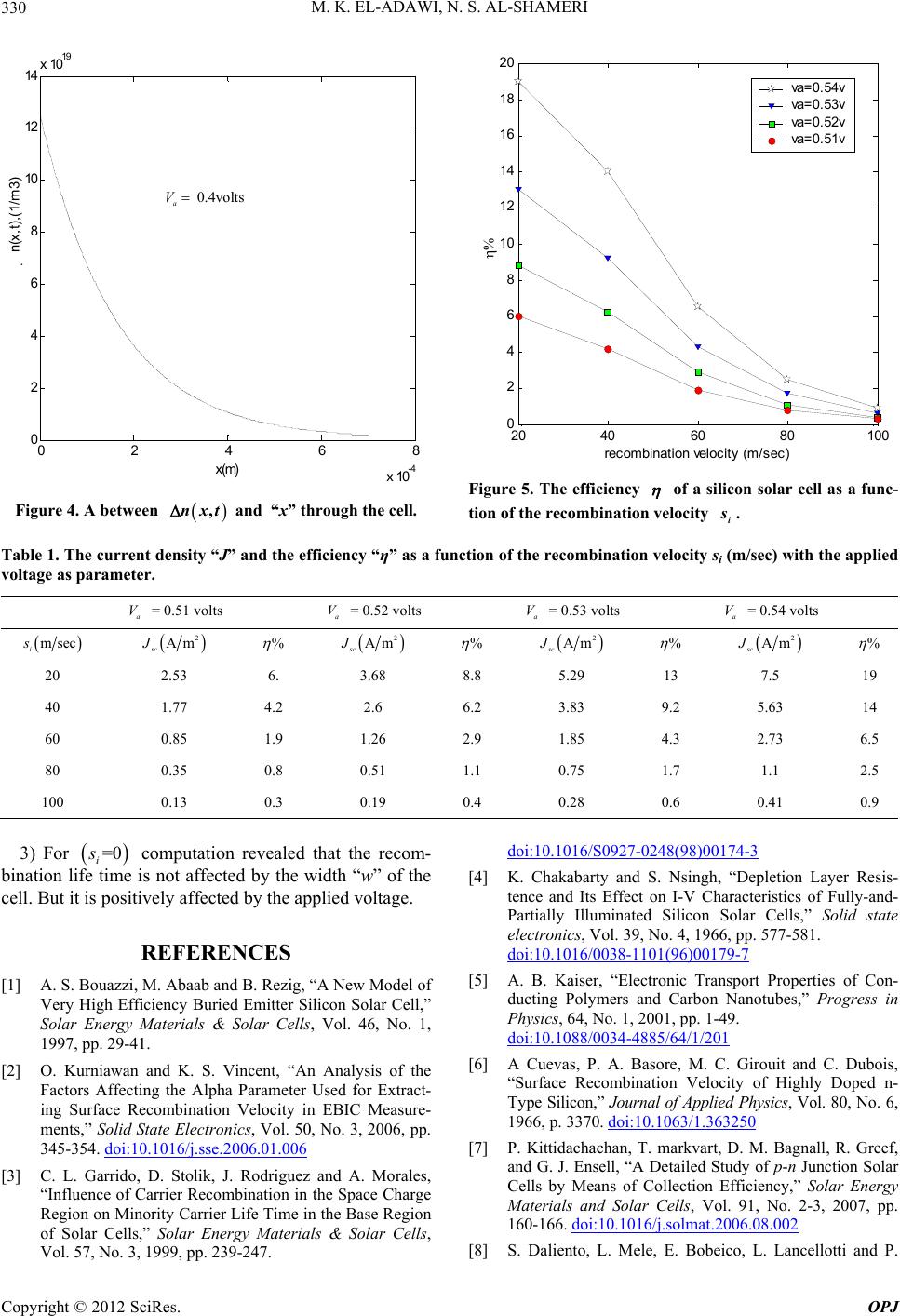 M. K. EL-ADAWI, N. S. AL-SHAMERI Copyright © 2012 SciRes. OPJ 330 20 4060 80100 0 2 4 6 8 10 12 14 16 18 20 recombination velocit y (m/s ec) va=0.54v va=0.53v va=0.52v va=0.51v 0246 8 x 1 0-4 0 2 4 6 8 10 12 14 x 1019 x(m) n( x,t),(1/m3) 0.4volts a V Figure 5. The efficiency of a silicon solar cell as a func- tion of the recombination velocity . i s Figure 4. A between “x” through the cell. ,and nxt Table 1. The current density “J” and the efficiency “η” as a function of the recombination velocity si (m/sec) with the applied voltage as parameter. a V = 0.51 volts a V = 0.52 volts a V = 0.53 volts a V = 0.54 volts msec i s 2 Am sc J % 2 Am sc J % 2 Am sc J % 2 Am sc J % 20 2.53 6. 3.68 8.8 5.29 13 7.5 19 40 1.77 4.2 2.6 6.2 3.83 9.2 5.63 14 60 0.85 1.9 1.26 2.9 1.85 4.3 2.73 6.5 80 0.35 0.8 0.51 1.1 0.75 1.7 1.1 2.5 100 0.13 0.3 0.19 0.4 0.28 0.6 0.41 0.9 3) For computation revealed that the recom- bination life time is not affected by the width “w” of the cell. But it is positively affected by the applied voltage. =0 i s REFERENCES [1] A. S. Bouazzi, M. Abaab and B. Rezig, “A New Model of Very High Efficiency Buried Emitter Silicon Solar Cell,” Solar Energy Materials & Solar Cells, Vol. 46, No. 1, 1997, pp. 29-41. [2] O. Kurniawan and K. S. Vincent, “An Analysis of the Factors Affecting the Alpha Parameter Used for Extract- ing Surface Recombination Velocity in EBIC Measure- ments,” Solid State Electronics, Vol. 50, No. 3, 2006, pp. 345-354. doi:10.1016/j.sse.2006.01.006 [3] C. L. Garrido, D. Stolik, J. Rodriguez and A. Morales, “Influence of Carrier Recombination in the Space Charge Region on Minority Carrier Life Time in the Base Region of Solar Cells,” Solar Energy Materials & Solar Cells, Vol. 57, No. 3, 1999, pp. 239-247. doi:10.1016/S0927-0248(98)00174-3 [4] K. Chakabarty and S. Nsingh, “Depletion Layer Resis- tence and Its Effect on I-V Characteristics of Fully-and- Partially Illuminated Silicon Solar Cells,” Solid state electronics, Vol. 39, No. 4, 1966, pp. 577-581. doi:10.1016/0038-1101(96)00179-7 [5] A. B. Kaiser, “Electronic Transport Properties of Con- ducting Polymers and Carbon Nanotubes,” Progress in Physics, 64, No. 1, 2001, pp. 1-49. doi:10.1088/0034-4885/64/1/201 [6] A Cuevas, P. A. Basore, M. C. Girouit and C. Dubois, “Surface Recombination Velocity of Highly Doped n- Type Silicon,” Journal of Applied Physics, Vol. 80, No. 6, 1966, p. 3370. doi:10.1063/1.363250 [7] P. Kittidachachan, T. markvart, D. M. Bagnall, R. Greef, and G. J. Ensell, “A Detailed Study of p-n Junction Solar Cells by Means of Collection Efficiency,” Solar Energy Materials and Solar Cells, Vol. 91, No. 2-3, 2007, pp. 160-166. doi:10.1016/j.solmat.2006.08.002 [8] S. Daliento, L. Mele, E. Bobeico, L. Lancellotti and P. 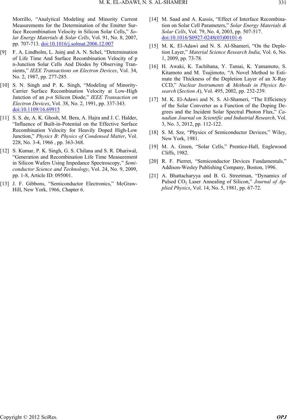 M. K. EL-ADAWI, N. S. AL-SHAMERI 331 Morrillo, “Analytical Modeling and Minority Current Measurements for the Determination of the Emitter Sur- face Recombination Velocity in Silicon Solar Cells,” So- lar Energy Materials & Solar Cells, Vol. 91, No. 8, 2007, pp. 707-713. doi:10.1016/j.solmat.2006.12.007 [9] F. A. Lindholm, L. Juinj and A. N. Schel, “Determination of Life Time And Surface Recombination Velocity of p n-Junction Solar Cells And Diodes by Observing Tran- sients,” IEEE Transactions on Electron Devices, Vol. 34, No. 2, 1987, pp. 277-285. [10] S. N. Singh and P. K. Singh, “Modeling of Minority- Carrier Surface Recombination Velocity at Low-High Junction of an p-n Silicon Diode,” IEEE Transaction on Electron Devi ces, Vol. 38, No. 2, 1991, pp. 337-343. doi:10.1109/16.69915 [11] S. S. de, A. K. Ghosh, M. Bera, A. Hajra and J. C. Halder, “Influence of Built-in-Potential on the Effective Surface Recombination Velocity for Heavily Doped High-Low Junction,” Physics B: Physics of Condensed Matter, Vol. 228, No. 3-4, 1966 , pp. 363-368. [12] S. Kumar, P. K. Singh, G. S. Chilana and S. R. Dhariwal, “Generation and Recombination Life Time Measurement in Silicon Wafers Using Impedance Spectroscopy,” Semi- conductor Science and Technology, Vol. 24, No. 9, 2009, pp. 1-8, Article ID: 095001. [13] J. F. Gibbons, “Semiconductor Electronics,” McGraw- Hill, New York, 1966, Chapter 6. [14] M. Saad and A. Kassis, “Effect of Interface Recombina- tion on Solar Cell Parameters,” Solar Energy Materials & Solar Cells, Vol. 79, No. 4, 2003, pp. 507-517. doi:10.1016/S0927-0248(03)00101-6 [15] M. K. El-Adawi and N. S. Al-Shameri, “On the Deple- tion Layer,” Material Science Research India, Vol. 6, No. 1, 2009, pp. 73-78. [16] H. Awaki, K. Tachibana, Y. Tamai, K. Yamamoto, S. Kitamoto and M. Tsujimoto, “A Novel Method to Esti- mate the Thickness of the Depletion Layer of an X-Ray CCD,” Nuclear Instruments & Methods in Physics Re- search (Sect ion A), Vol. 495, 2002, pp. 232-239. [17] M. K. El-Adawi and N. S. Al-Shameri, “The Efficiency of the Solar Converter as a Function of the Doping De- grees and the Incident Solar Spectral Photon Flux,” Ca- nadian Journal on Scientific and Industrial Research, Vol. 3, No. 3, 2012, pp. 112-122. [18] S. M. Sze, “Physics of Semiconductor Devices,” Wiley, New York, 1981. [19] M. A. Green, “Solar Cells,” Prentice-Hall, Englewood Cliffs, 1982. [20] R. F. Pierret, “Semiconductor Devices Fundamentals,” Addison-Wesley Publishing Company, Boston, 1996. [21] A. Bhattacharyya and B. G. Streetman, “Dynamics of Pulsed CO2 Laser Annealing of Silicon,” Journal of Ap- plied Physics, Vol. 14, No. 5, 1981, pp. 67-72. Copyright © 2012 SciRes. OPJ
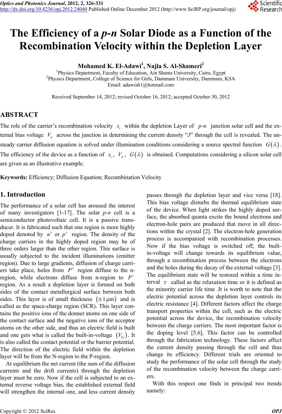
|