 Optics and Photonics Journal, 2012, 2, 300-313 http://dx.doi.org/10.4236/opj.2012.24037 Published Online December 2012 (http://www.SciRP.org/journal/opj) Fully On-Chip Integrated Photodetector Front-End Dedicated to Real-Time Portable Optical Brain Imaging Ehsan Kamrani, Frederic Lesage, Mohamad Sawan Electrical Engineering Department, Ecole Polytechnique, Montreal, Canada Email: ehsan.kamrani@polymtl.ca Received August 10, 2012; revised September 13, 2012; accepted September 28, 2012 ABSTRACT Optical brain imaging using functional near infra-red spectroscopy (fNIRS) offers a portable and noninvasive tool for monitoring of blood oxygenation. In this paper we have introduced a new miniaturized photodetector front-end on a chip to be applied in a portable fNIRS system. It includes silicon avalanche photodiodes (SiAPD), Transimpedance am- plifier (TIA) front-end and Quench-Reset circuitry to operate in both linear and Geiger modes. So it can be applied for both continuous-wave fNIRS (CW-fNIRS) and also single-photon counting. Proposed SiAPD exhibits high-avalanche gain (>100), low-breakdown voltage (<12 V) and high photon detection efficiency accompanying with low dark count rates. The proposed TIA front-end offer a low power consumption (<1 mW), high-transimpedance gain (up to 250 MV/A), tunable bandwidth (1 kHz - 1 GHz) and very low input and output noise (~few fA/√Hz and few µV/√Hz). The Geiger-mode photon counting front-end also exhibits a controllable hold-off and rest time with an ultra fast quench- reset time (few ns). This integrated system has been implemented using submicron (0.35 µm) standard CMOS technol- ogy. Keywords: Biochip; Analog CMOS Integrated Circuit; Trans-Impedance Amplifier; fNIRS; Brain Imaging; Medical Imaging; Optical Sensors 1. Introduction Optical sensors and systems are widely applied in bio- logical and biomedical imaging. Optical coherent tomo- graphy (OCT), pulse-oximetry, Brillouin scattering (BLS) imaging, Optical dermatology, and spectroscopy are some examples. Common brain monitoring systems are bulky, non-portable and invasive and require sophisti- cated and expensive hardware and software tools [1], so they are not a proper platform to be developed as a port- able brain imaging system. The commonly used non- invasive brain imaging techniques are electro-encepha- lography (EEG), magneto-encephalography (MEG), po- sitron emission tomography (PET), functional magnetic resonance imaging (fMRI), and functional near-infrared spectroscopy (fNIRS) [2]. Only EEG and fNIRS can be realized using equipment that is small and light enough to be worn continuously while allowing body move- ments. However some portable EEG systems has been de- veloped currently for brain imaging [3], EEG is not ideal for human-computer interface (HCI) [4], it is susceptible to artifacts from eye and facial movement, as well as near by electronic devices, it requires gel in the participant’s hair, it takes time to setup properly and is not spatially determined [5]. We are applying fNIRS to develop a portable tool for real-time brain imaging. fNIRS is a non-invasive, minimally intrusive, safe, and high-tem- poral resolution imaging technique for real-time and long- term monitoring of the brain function and biological tis- sues. It is considered as one of the most efficient diagno- sis and investigation techniques of different neurological diseases, such as, stroke and epilepsy seizures that re- quire continuous monitoring of the patient at the hospital, which is a costly endeavor. In contrast to the other bulky and high-voltage brain imaging systems suffering from electromagnetic interfaces and slight movement artifacts, fNIRS is portable, low-voltage and immune to electro- magnetic interferences with the advantages of ease of use and short setup time [5]. In fNIRS, the brain tissue is penetrated by near-infrared (NIR) radiation and the re- flected signal is observed to investigate the brain func- tion. In NIR range (650 nm - 950 nm), water has rela- tively low absorption while oxy- and deoxy-hemoglobin have high absorption. Due to these properties, NIR light can penetrate bio- logical tissues in the range of 0.5 - 3 cm allowing inves- tigation of relatively deep brain tissues, and ability to differentiate between healthy and diseased tissues based on their optical properties. The typical CW-fNIRS sys- tem consists of NIR light source, photodetector, data C opyright © 2012 SciRes. OPJ  E. KAMRANI ET AL. 301 Emitter IR Transmitter Computer Demodulator/ Amplifier IR Receiver Driver/ Modulator Photoreceiver Data Acquisition Processing/ Storage (a) (b) Figure 1. Block diagram of a typical portable wireless fNIRS (a) and the phototransceiver front-end building blocks (b). acquisition module and control unit, and a processing block (Figure 1(a)). The light source is placed on the surface of the head (scalp) and it generates light in the NIR range. Generally, the light sources used for NIRS system are either LEDs or laser diodes that emit NIR light with optical power within a range of 5 mW to 17 mW at discrete wavelengths (for example 735, 840, and 940 nm). The fNIRS photodetector front-end includes a photodetector that monitors the intensity of the reflected NIR signal, Quench-Reset Circuit, Trans-impedance Am- plifier (TIA), Limiting Amplifier, post amplifiers and filters (Figure 1(b)). Although fNIRS is compact when compared to other brain imaging systems, but current commercially available NIRS devices are still too bulky to be wearable or portable for monitoring brain function. They are not miniaturized enough in order to be inte- grated with other wireless and portable medical imaging systems intended for bedside real-time brain monitoring. It also suffers from low spatial resolution, high-level noise, susceptible to the internal and ambient light/tem- perature and bias voltage variations. In this paper we propose a miniaturized, reconfigu- rable, low-power, low-noise and high-gain fNIRS photo- receiver for real-time brain imaging. Integrating the pho- todiode and corresponding circuitries on the same chip and on-chip multi-mode operation using smart CMOS image sensor concept has not been considered yet in lit- erature for fNIRS application. Using smart CMOS im- age sensor concept for fabrication of photodiode and photodetection circuitry and integrating them on the same chip with ability to work on different modes of operations, leads to a more compact and miniaturized design. Using p+/n-well topology with guard-ring and negative feedback avalanche concept in fabrication of photodiode, we have designed a photodiode with high detection efficiency and low-noise using standard CMOS process. An integrated low-noise, high-gain and low- power photodetector TIA front-end and an ultra-fast quench-reset front-end also have been introduced in this paper. The remaining parts of this paper are organized as fol- lows. First the implementation of the CMOS photodetec- tor is described at Section 2. The integrated electronics front-ends for linear and Geiger modes of operation are introduced in Sections 3 and 4 respectively. Section 5 depicts the general characteristics of the integrated sys- tem. 2. Design of CMOS SiAPDs as Image Sensor Conventional photodetectors use photon multiplier tubes (PMTs) which are bulky, subtle, sensitive to magnetic fields and require high-supply voltage [6]. The photo- diode used in the photodetector requires being highly sensitive, enabling the reliable conversion of the ultra- low amplitude light signal into a detectable electric sig- nal. Silicon avalanche photodiode (SiAPD) is a potential candidate for low-level light detection in the visible and near-infrared regions due to its bias dependent internal Copyright © 2012 SciRes. OPJ  E. KAMRANI ET AL. 302 gain and its ability to amplify the photogenerated signal by avalanche multiplication [7]. The SiAPDs fabricated in dedicated process have two major disadvantages: the production cost is very high due to the specialized fabrication process, and the impossibil- ity to integrate electronic circuits on the same chip. Op- timizing the performance of both the CMOS devices and the SiAPD is a challenging task. To overcome these problems, researchers have investigated the design and fabrication of SiAPDs in a standard CMOS process [8,9]. The advantages of standard CMOS fabrication process are: the availability of a fully supported, mature and re- liable technology at reasonably low cost, and the possi- bility of developing a complete system on chip with a high degree of complexity [10-12]. The mandatory requirement for SiAPD fabrication in standard CMOS process is that a suitable subset of CMOS fabrication process flow should be able to build a planar p-n junction without device breakdown at the photodiode periphery. SiAPDs fabricated using standard CMOS process involves high doped p or n layer resulting in shallow or medium depth depletion region. As a con- sequence, CMOS SiAPDs are inefficient to detect red and NIR photons, and are not suitable for NIR signal detection in neuroimaging. However, to increase the use of SiAPD-based front-end receivers for biomedical ap- plications, integration of the SiAPD and peripheral cir- cuitry on the same chip using standard CMOS technol- ogy is highly desired. The fabrication of SiAPDs in standard CMOS technology permits fabrication of both the photodetector and the necessary peripheral circuits on the same chip for an integrated system. This leads to fea- sibility of implementation of a portable brain imaging system which is highly desired. However, it is challeng- ing to make SiAPDs in CMOS technology due to lack of special fabrication steps [9], the punch-through, high tunneling and premature edge breakdown (PEB) effects [10,13] and also the trade-offs between several design parameters such as scale, shape, doping, noise, efficiency, gain, speed, etc.. High-level noise and low-efficiency of the currently available detectors [7,8], encourages us to design a new SiAPD with low-noise and high detection efficiency at NIR region [13-15]. Here we have designed the p+/n-well SiAPDs with different guard rings (n-well and p-well) in different shapes and scales. These provide a tradeoff between fill factor and angularity and a feasible way to validate the efficiency of the applied guard-rings. The p-well APD is a p+/n-well APD developed in square and octagonal shape with p-well guard ring to preventing PEBs. The guard ring is achieved by low doped p-well around p+ active area with 100 µm diameter (Figure 2(a)). Another new photodiode (APD2) which is an n+/p-sub SiAPD with n-well PEB prevention (PEBP) technique (Figure 2(b)). It uses the connection between the highly doped n region and the substrate as the active region. Optimiza- tion of the performance of SiAPD is done by device level simulation using Sentaurus TCAD software. The active junction of the photodiode exists between p + (Na = 5 × 10¹⁹/cm3) and deep n-well (Nd = 1.28 × 10¹⁷/cm3). The main characteristics of these APDs are shown in Table 1. The photon detection probability (PDP) and the sensitiv- ity of the APDs also are plated and compared in Figure 3. The results show a higher PDP and sensitivity of the p-well APD comparing to APD2. 3. Geiger-Mode Front-End Implementation A diode working in the region near the breakdown volt- age can be applied in two different modes of operations: Proportional (linear or amplification) mode and Geiger (digital or trigger) mode. In Geiger mode, SiAPDs work as trigger devices rather than amplifying devices. For operating the SiAPD in Geiger mode (single photon counting mode) quenching and reset circuits are neces- sary. Generally three types of quenching circuits have been used for Geiger mode operation: passive, active and mixed quenching circuits. Passive quenching (PQ) is suitable for APDs having small area and small RC time contacts since it can be operated at higher speed. The schematic of two possible configurations of passive quench circuits [16-20] are shown in Figure 4. In Figures 4(b) and (c) the APD cathode voltage and current in response to single photon arrival are plotted. They can also be used with large area devices where high counting rates are not a requirement. Since we require large area APDs for our application that is expected to count photons at high-speed (≥1 MHz), PQ is not a feasible option. p-sub n-well n+ n+ p+ (active area) D eep n-w ell poly polyMetal RingMeta l Ring n-welln-wellp-wellp-well (a) p-sub n-well n+ n+ p+ (active area)d Deep n-w ell poly polyMetal RingMetal Ring n-well d n-well (b) Figure 2. Cross-section of the proposed APDs: (a) The p- well (APD1) and (b) The p-sub (APD2). Copyright © 2012 SciRes. OPJ  E. KAMRANI ET AL. Copyright © 2012 SciRes. OPJ 303 Table 1. The characteristics of the proposed SiAPDs. SiAPD p-well (APD1) p-sub (APD2) Reference Parameter Rectangular Rectangular Rectangular Octagonal Linear Gain 200 220 140 100 Area(~µm2) 100 × 100 400 × 400 100 × 100 100 ×100 PDE @550 nm 45% 75% 22% 52% F@M = 20 89@800nm 60@800nm 59@800nm 138@800nm Impedance (Ω) 600 600 0.5 0.5 Capacitance 1pF 30 pF 1pF 1pF (a) (b) Figure 3. Comparison of different implemented APDs: (a) PDP and (b) Sensitivity. of the circuit does not depend on the component values and can be accurately controlled, hence determination of precise dead time is possible for satisfactory circuit op- eration [12]. However, it is difficult to design an effec- tive AQC and it needs extra and complicated ultra-pre- cise circuitry to reduce propagation delays as well as stray capacitances. In order to achieve faster quenching, active quenching circuit (AQC) is used [11]. This method forces back on the APD to drop the bias voltage much quicker enabling significant speed improvements over the PQ method. It causes high accuracy in photon timing. Small delay in quenching the avalanche resulting in fewer carriers crossing the junction and hence low false re-triggering of avalanche (lower after pulse). This also results in lower power loss and hence less heating of the APD. Dead time Using proposed mixed quench circuit (MQC), depicted in Figure 5 [12], reduces the required size of load resistor 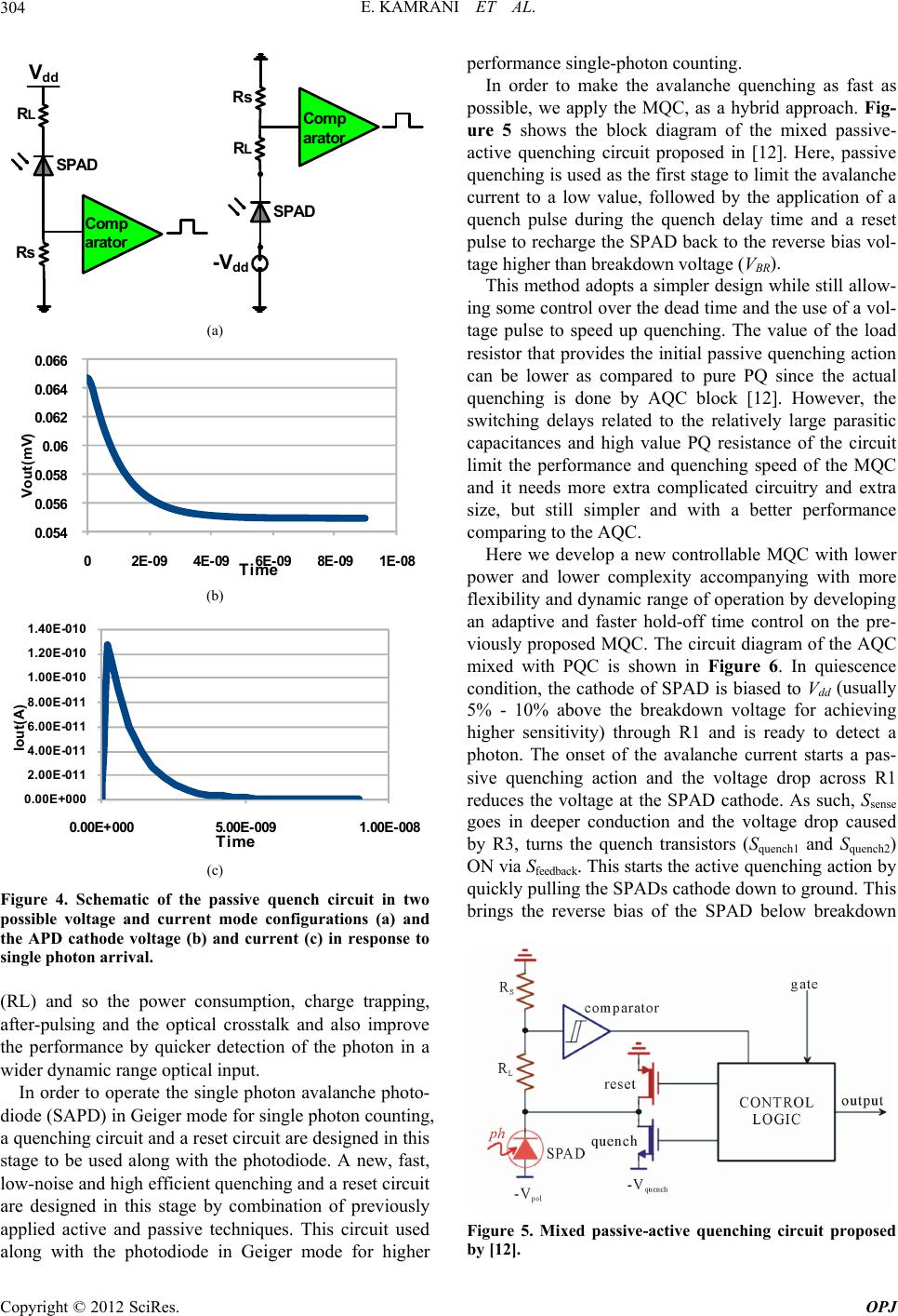 E. KAMRANI ET AL. 304 Comp arator RL Rs Vdd SPAD SPAD Comp arat or Rs RL -Vdd (a) 0.054 0.056 0.058 0.06 0.062 0.064 0.066 02E-09 4E-09 6E-09 8E-09 1E-08 Vout (mV) Time (b) 0.00E+000 2.00E-011 4.00E-011 6.00E-011 8.00E-011 1.00E-010 1.20E-010 1.40E-010 0.00E+000 5.00E-0091.00E-008 Iout(A) Time (c) Figure 4. Schematic of the passive quench circuit in two possible voltage and current mode configurations (a) and the APD cathode voltage (b) and current (c) in response to single photon arrival. (RL) and so the power consumption, charge trapping, after-pulsing and the optical crosstalk and also improve the performance by quicker detection of the photon in a wider dynamic range optical input. In order to operate the single photon avalanche photo- diode (SAPD) in Geiger mode for single photon counting, a quenching circuit and a reset circuit are designed in this stage to be used along with the photodiode. A new, fast, low-noise and high efficient quenching and a reset circuit are designed in this stage by combination of previously applied active and passive techniques. This circuit used along with the photodiode in Geiger mode for higher performance single-photon counting. In order to make the avalanche quenching as fast as possible, we apply the MQC, as a hybrid approach. Fig- ure 5 shows the block diagram of the mixed passive- active quenching circuit proposed in [12]. Here, passive quenching is used as the first stage to limit the avalanche current to a low value, followed by the application of a quench pulse during the quench delay time and a reset pulse to recharge the SPAD back to the reverse bias vol- tage higher than breakdown voltage (VBR). This method adopts a simpler design while still allow- ing some control over the dead time and the use of a vol- tage pulse to speed up quenching. The value of the load resistor that provides the initial passive quenching action can be lower as compared to pure PQ since the actual quenching is done by AQC block [12]. However, the switching delays related to the relatively large parasitic capacitances and high value PQ resistance of the circuit limit the performance and quenching speed of the MQC and it needs more extra complicated circuitry and extra size, but still simpler and with a better performance comparing to the AQC. Here we develop a new controllable MQC with lower power and lower complexity accompanying with more flexibility and dynamic range of operation by developing an adaptive and faster hold-off time control on the pre- viously proposed MQC. The circuit diagram of the AQC mixed with PQC is shown in Figure 6. In quiescence condition, the cathode of SPAD is biased to Vdd (usually 5% - 10% above the breakdown voltage for achieving higher sensitivity) through R1 and is ready to detect a photon. The onset of the avalanche current starts a pas- sive quenching action and the voltage drop across R1 reduces the voltage at the SPAD cathode. As such, Ssense goes in deeper conduction and the voltage drop caused by R3, turns the quench transistors (Squench1 and Squench2) ON via Sfeedback. This starts the active quenching action by quickly pulling the SPADs cathode down to ground. This brings the reverse bias of the SPAD below breakdown Figure 5. Mixed passive-active quenching circuit proposed by [12]. Copyright © 2012 SciRes. OPJ 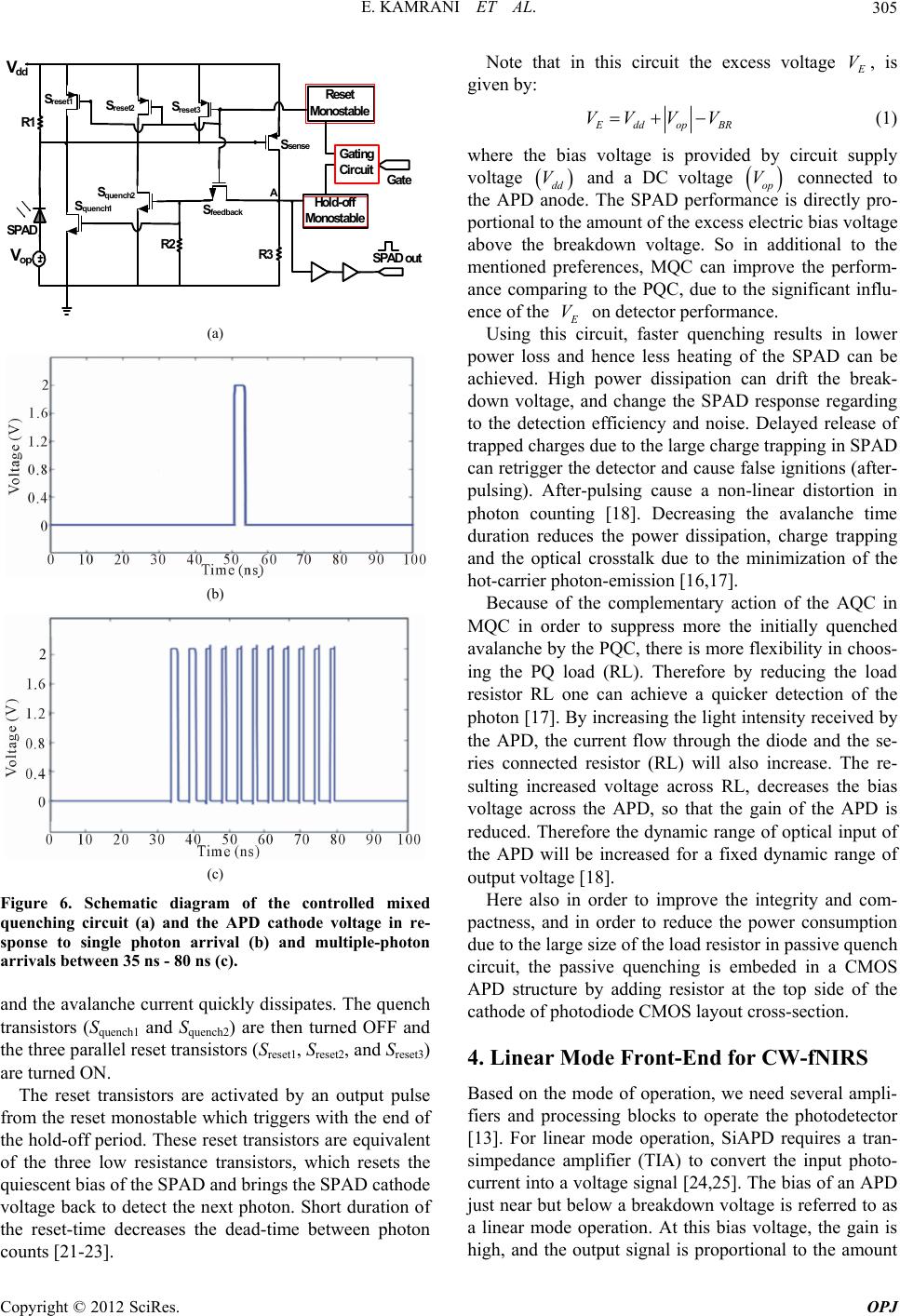 E. KAMRANI ET AL. 305 Reset Monostable Gate Vop H o ld -o ff Monostable R2 R1 R3 Sreset1 Sreset2 Sreset3 Ssense Squench1 Squench2Sfeedback Vdd SPAD out Gating Cir cuit SPAD + A (a) (b) (c) Figure 6. Schematic diagram of the controlled mixed quenching circuit (a) and the APD cathode voltage in re- sponse to single photon arrival (b) and multiple-photon arrivals between 35 ns - 80 ns (c). and the avalanche current quickly dissipates. The quench transistors (Squench1 and Squench2) are then turned OFF and the three parallel reset transistors (Sreset1, Sreset2, and Sreset3) are turned ON. The reset transistors are activated by an output pulse from the reset monostable which triggers with the end of the hold-off period. These reset transistors are equivalent of the three low resistance transistors, which resets the quiescent bias of the SPAD and brings the SPAD cathode voltage back to detect the next photon. Short duration of the reset-time decreases the dead-time between photon counts [21-23]. Note that in this circuit the excess voltage V, is given by: ddop BR VVV V (1) where the bias voltage is provided by circuit supply voltage dd V and a DC voltage connected to the APD anode. The SPAD performance is directly pro- portional to the amount of the excess electric bias voltage above the breakdown voltage. So in additional to the mentioned preferences, MQC can improve the perform- ance comparing to the PQC, due to the significant influ- ence of the op V V on detector performance. Using this circuit, faster quenching results in lower power loss and hence less heating of the SPAD can be achieved. High power dissipation can drift the break- down voltage, and change the SPAD response regarding to the detection efficiency and noise. Delayed release of trapped charges due to the large charge trapping in SPAD can retrigger the detector and cause false ignitions (after- pulsing). After-pulsing cause a non-linear distortion in photon counting [18]. Decreasing the avalanche time duration reduces the power dissipation, charge trapping and the optical crosstalk due to the minimization of the hot-carrier photon-emission [16,17]. Because of the complementary action of the AQC in MQC in order to suppress more the initially quenched avalanche by the PQC, there is more flexibility in choos- ing the PQ load (RL). Therefore by reducing the load resistor RL one can achieve a quicker detection of the photon [17]. By increasing the light intensity received by the APD, the current flow through the diode and the se- ries connected resistor (RL) will also increase. The re- sulting increased voltage across RL, decreases the bias voltage across the APD, so that the gain of the APD is reduced. Therefore the dynamic range of optical input of the APD will be increased for a fixed dynamic range of output voltage [18]. Here also in order to improve the integrity and com- pactness, and in order to reduce the power consumption due to the large size of the load resistor in passive quench circuit, the passive quenching is embeded in a CMOS APD structure by adding resistor at the top side of the cathode of photodiode CMOS layout cross-section. 4. Linear Mode Front-End for CW-fNIRS Based on the mode of operation, we need several ampli- fiers and processing blocks to operate the photodetector [13]. For linear mode operation, SiAPD requires a tran- simpedance amplifier (TIA) to convert the input photo- current into a voltage signal [24,25]. The bias of an APD just near but below a breakdown voltage is referred to as a linear mode operation. At this bias voltage, the gain is high, and the output signal is proportional to the amount Copyright © 2012 SciRes. OPJ 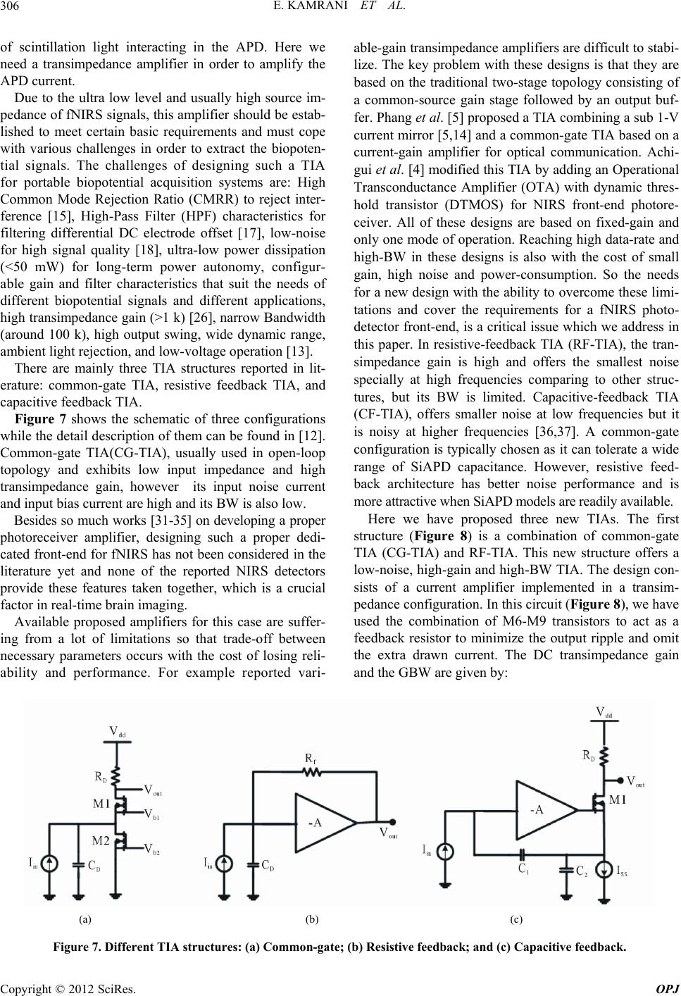 E. KAMRANI ET AL. Copyright © 2012 SciRes. OPJ 306 of scintillation light interacting in the APD. Here we need a transimpedance amplifier in order to amplify the APD current. able-gain transimpedance amplifiers are difficult to stabi- lize. The key problem with these designs is that they are based on the traditional two-stage topology consisting of a common-source gain stage followed by an output buf- fer. Phang et al. [5] proposed a TIA combining a sub 1-V current mirror [5,14] and a common-gate TIA based on a current-gain amplifier for optical communication. Achi- gui et al. [4] modified this TIA by adding an Operational Transconductance Amplifier (OTA) with dynamic thres- hold transistor (DTMOS) for NIRS front-end photore- ceiver. All of these designs are based on fixed-gain and only one mode of operation. Reaching high data-rate and high-BW in these designs is also with the cost of small gain, high noise and power-consumption. So the needs for a new design with the ability to overcome these limi- tations and cover the requirements for a fNIRS photo- detector front-end, is a critical issue which we address in this paper. In resistive-feedback TIA (RF-TIA), the tran- simpedance gain is high and offers the smallest noise specially at high frequencies comparing to other struc- tures, but its BW is limited. Capacitive-feedback TIA (CF-TIA), offers smaller noise at low frequencies but it is noisy at higher frequencies [36,37]. A common-gate configuration is typically chosen as it can tolerate a wide range of SiAPD capacitance. However, resistive feed- back architecture has better noise performance and is more attractive when SiAPD models are readily available. Due to the ultra low level and usually high source im- pedance of fNIRS signals, this amplifier should be estab- lished to meet certain basic requirements and must cope with various challenges in order to extract the biopoten- tial signals. The challenges of designing such a TIA for portable biopotential acquisition systems are: High Common Mode Rejection Ratio (CMRR) to reject inter- ference [15], High-Pass Filter (HPF) characteristics for filtering differential DC electrode offset [17], low-noise for high signal quality [18], ultra-low power dissipation (<50 mW) for long-term power autonomy, configur- able gain and filter characteristics that suit the needs of different biopotential signals and different applications, high transimpedance gain (>1 k) [26], narrow Bandwidth (around 100 k), high output swing, wide dynamic range, ambient light rejection, and low-voltage operation [13]. There are mainly three TIA structures reported in lit- erature: common-gate TIA, resistive feedback TIA, and capacitive feedback TIA. Figure 7 shows the schematic of three configurations while the detail description of them can be found in [12]. Common-gate TIA(CG-TIA), usually used in open-loop topology and exhibits low input impedance and high transimpedance gain, however its input noise current and input bias current are high and its BW is also low. Here we have proposed three new TIAs. The first structure (Figure 8) is a combination of common-gate TIA (CG-TIA) and RF-TIA. This new structure offers a low-noise, high-gain and high-BW TIA. The design con- sists of a current amplifier implemented in a transim- pedance configuration. In this circuit (Figure 8), we have used the combination of M6-M9 transistors to act as a feedback resistor to minimize the output ripple and omit the extra drawn current. The DC transimpedance gain and the GBW are given by: Besides so much works [31-35] on developing a proper photoreceiver amplifier, designing such a proper dedi- cated front-end for fNIRS has not been considered in the literature yet and none of the reported NIRS detectors provide these features taken together, which is a crucial factor in real-time brain imaging. Available proposed amplifiers for this case are suffer- ing from a lot of limitations so that trade-off between necessary parameters occurs with the cost of losing reli- ability and performance. For example reported vari- (a) (b) (c) Figure 7. Different TIA structures: (a) Common-gate; (b) Resistive feedback; and (c) Capacitive feedback. 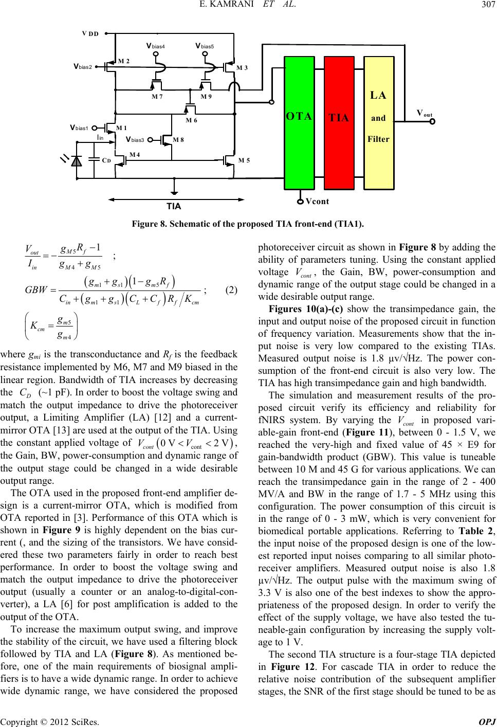 E. KAMRANI ET AL. 307 M4 M2 M1 M3 VDD M6 M7 CDM5 M8 Vbias1 Vbias2 Vbias3 Vbias4 Iin Vcont OTA TIA LA and Filter Vout TIA M9 Vbias5 Figure 8. Schematic of the proposed TIA front-end (TIA1). 5 45 11 5 11 5 4 1; 1; Mf out inM M ms mf inmsLf fcm m cm m R g V Igg gg gR GBW CggCCRK g Kg (2) where gmi is the transconductance and Rf is the feedback resistance implemented by M6, M7 and M9 biased in the linear region. Bandwidth of TIA increases by decreasing the C (~1 pF). In order to boost the voltage swing and match the output impedance to drive the photoreceiver output, a Limiting Amplifier (LA) [12] and a current- mirror OTA [13] are used at the output of the TIA. Using the constant applied voltage of , the Gain, BW, power-consumption and dynamic range of the output stage could be changed in a wide desirable output range. cont 0V 2V cont VV The OTA used in the proposed front-end amplifier de- sign is a current-mirror OTA, which is modified from OTA reported in [3]. Performance of this OTA which is shown in Figure 9 is highly dependent on the bias cur- rent (, and the sizing of the transistors. We have consid- ered these two parameters fairly in order to reach best performance. In order to boost the voltage swing and match the output impedance to drive the photoreceiver output (usually a counter or an analog-to-digital-con- verter), a LA [6] for post amplification is added to the output of the OTA. To increase the maximum output swing, and improve the stability of the circuit, we have used a filtering block followed by TIA and LA (Figure 8). As mentioned be- fore, one of the main requirements of biosignal ampli- fiers is to have a wide dynamic range. In order to achieve wide dynamic range, we have considered the proposed photoreceiver circuit as shown in Figure 8 by adding the ability of parameters tuning. Using the constant applied voltage cont , the Gain, BW, power-consumption and dynamic range of the output stage could be changed in a wide desirable output range. V Figures 10(a)-(c) show the transimpedance gain, the input and output noise of the proposed circuit in function of frequency variation. Measurements show that the in- put noise is very low compared to the existing TIAs. Measured output noise is 1.8 µv/√Hz. The power con- sumption of the front-end circuit is also very low. The TIA has high transimpedance gain and high bandwidth. The simulation and measurement results of the pro- posed circuit verify its efficiency and reliability for fNIRS system. By varying the cont V in proposed vari- able-gain front-end (Figure 11), between 0 - 1.5 V, we reached the very-high and fixed value of 45 × E9 for gain-bandwidth product (GBW). This value is tuneable between 10 M and 45 G for various applications. We can reach the transimpedance gain in the range of 2 - 400 MV/A and BW in the range of 1.7 - 5 MHz using this configuration. The power consumption of this circuit is in the range of 0 - 3 mW, which is very convenient for biomedical portable applications. Referring to Table 2, the input noise of the proposed design is one of the low- est reported input noises comparing to all similar photo- receiver amplifiers. Measured output noise is also 1.8 µv/√Hz. The output pulse with the maximum swing of 3.3 V is also one of the best indexes to show the appro- priateness of the proposed design. In order to verify the effect of the supply voltage, we have also tested the tu- neable-gain configuration by increasing the supply volt- age to 1 V. The second TIA structure is a four-stage TIA depicted in Figure 12. For cascade TIA in order to reduce the relative noise contribution of the subsequent amplifier stages, the SNR of the first stage should be tuned to be as Copyright © 2012 SciRes. OPJ 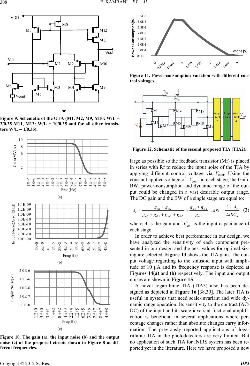 E. KAMRANI ET AL. 308 VDD M7 M8 M5 M3 M6 M4 M9 M2 M1 M12 M10 M11 Vcont Vout Vi n Figure 9. Schematic of the OTA (M1, M2, M9, M10: W/L = 2/0.35 M11, M12: W/L = 10/0.35 and for all other transis- tors W/L = 1/0.35). 2 4 6 8 10 1E+0 3E+0 1E+1 4E+1 1E+2 5E+2 2E+3 6E+3 2E+4 7E+4 3E+5 9E+5 3E+6 1E+7 4E+7 1E+8 4E+8 Gain(MV/A) Freq(Hz ) (a) 0.0 E+00 2.0E-10 4.0E-10 6.0E-10 8.0E-10 1.0E-09 1.2E-09 1.4E-09 1E+0 5E+0 3E+1 1E+2 8E+2 4E+3 2E+4 1E+5 6E+5 3E+6 2E+7 8E+7 4E+8 Input Noise(A/sqrt(Hz)) Freq(Hz) (b) 0.0E+0 5.0E-7 1.0E-6 1.5E-6 2.0E-6 1E+0 5E+0 3E+1 1E+2 8E+2 4E+3 2E+4 1E+5 6E+5 3E+6 2E+7 8E+7 4E+8 Output Noise(V) Freq(Hz) (c) Figure 10. The gain (a), the input noise (b) and the output noise (c) of the proposed circuit shown in Figure 8 at dif- ferent frequencies. 0.0E+0 5.0E-4 1.0E-3 1.5E-3 2.0E-3 2.5E-3 3.0E-3 3.5E 3 Power Consumption(W) Vcont (V) Figure 11. Power-consumption variation with different con- trol voltages. Figure 12. Schematic of the second proposed TIA (TIA2). large as possible so the feedback transistor (Mf) is placed in series with Rf to reduce the input noise of the TIA by applying different control voltage via Vcont. Using the constant applied voltage of cont at each stage, the Gain, BW, power-consumption and dynamic range of the out- put could be changed in a vast desirable output range. The DC gain and the BW of a single stage are equal to: V 12 12 3123 3 1 ;BW2π mm mmi i mdsdsds min ggg AA ggg gRC (3) where A is the gain and is the input capacitance of each stage. in C In order to achieve best performance in our design, we have analyzed the sensitivity of each component pre- sented in our design and the best values for optimal siz- ing are selected. Figure 13 shows the TIA gain. The out- put voltage regarding to the sinusoid input with ampli- tude of 10 µA and its frequency response is depicted at Figures 14(a) and (b) respectively. The input and output noises are shown in Figure 15. A novel logarithmic TIA (TIA3) also has been de- signed as depicted in Figure 16 [38,39]. The later TIA is useful in systems that need scale-invariant and wide dy- namic range operation. Its sensitivity to the contrast (AC/ DC) of the input and its scale-invariant fractional amplifi- cation is beneficial in several applications where per- centage changes rather than absolute changes carry infor- mation. The previously reported applications of loga- rithmic TIA in the photodetectors are very limited. But no application of such TIA for fNIRS system has been re- ported yet in the literature. Here we have proposed a new Copyright © 2012 SciRes. OPJ 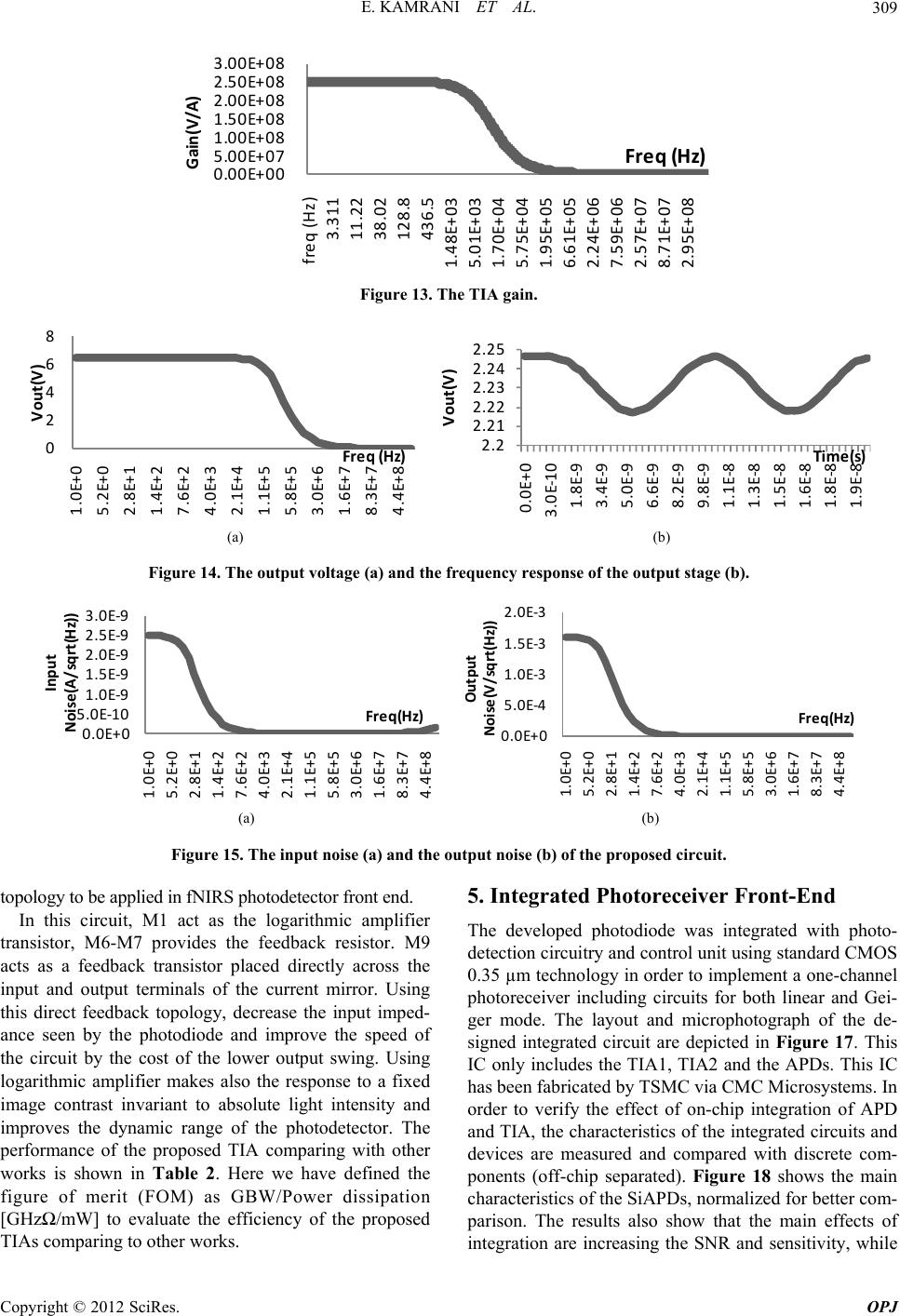 E. KAMRANI ET AL. Copyright © 2012 SciRes. OPJ 309 0.00E+00 5.00E+07 1.00E+08 1.50E+08 2.00E+08 2.50E+08 3.00E+08 freq (Hz) 3.311 11.22 38.02 128.8 436.5 1.48E+03 5.01E+03 1.70E+04 5.75E+04 1.95E+05 6.61E+05 2.24E+06 7.59E+06 2.57E+07 8.71E+07 2.95E+08 Gain(V/A) Freq (Hz) Figure 13. The TIA gain. 0 2 4 6 8 1.0E+0 5.2E+0 2.8E+1 1.4E+2 7.6E+2 4.0E+3 2.1E+4 1.1E+5 5.8E+5 3.0E+6 1.6E+7 8.3E+7 4.4E+8 Vout(V) Freq (Hz) 2.2 2.21 2.22 2.23 2.24 2.25 0.0E+ 0 3.0E-10 1.8E-9 3.4E-9 5.0E-9 6.6E-9 8.2E-9 9.8E-9 1.1E-8 1.3E-8 1.5E-8 1.6E-8 1.8E-8 1.9E-8 Vout(V) Time(s) (a) (b) Figure 14. The output voltage (a) and the frequency response of the output stage (b). 0.0E+0 5.0E-10 1.0E-9 1.5E-9 2.0E-9 2.5E-9 3.0E-9 1.0E+0 5.2E+0 2.8E+1 1.4E+2 7.6E+2 4.0E+3 2.1E+4 1.1E+5 5.8E+5 3.0E+6 1.6E+7 8.3E+7 4.4E+8 Input Noise (A /sq r t (Hz)) Freq(Hz) 0.0E+0 5.0E-4 1.0E-3 1.5E-3 2.0E-3 1.0E+ 0 5.2E+ 0 2.8E+ 1 1.4E+ 2 7.6E+ 2 4.0E+ 3 2.1E+ 4 1.1E+ 5 5.8E+ 5 3.0E+ 6 1.6E+ 7 8.3E+ 7 4.4E+ 8 Output Noise(V/sqrt(Hz)) Freq(Hz) (a) (b) Figure 15. The input noise (a) and the output noise (b) of the proposed circuit. 5. Integrated Photoreceiver Front-End topology to be applied in fNIRS photodetector front end. In this circuit, M1 act as the logarithmic amplifier transistor, M6-M7 provides the feedback resistor. M9 acts as a feedback transistor placed directly across the input and output terminals of the current mirror. Using this direct feedback topology, decrease the input imped- ance seen by the photodiode and improve the speed of the circuit by the cost of the lower output swing. Using logarithmic amplifier makes also the response to a fixed image contrast invariant to absolute light intensity and improves the dynamic range of the photodetector. The performance of the proposed TIA comparing with other works is shown in Table 2. Here we have defined the figure of merit (FOM) as GBW/Power dissipation The developed photodiode was integrated with photo- detection circuitry and control unit using standard CMOS 0.35 µm technology in order to implement a one-channel photoreceiver including circuits for both linear and Gei- ger mode. The layout and microphotograph of the de- signed integrated circuit are depicted in Figure 17. This IC only includes the TIA1, TIA2 and the APDs. This IC has been fabricated by TSMC via CMC Microsystems. In order to verify the effect of on-chip integration of APD and TIA, the characteristics of the integrated circuits and devices are measured and compared with discrete com- ponents (off-chip separated). Figure 18 shows the main characteristics of the SiAPDs, normalized for better com- parison. The results also show that the main effects of ntegration are increasing the SNR and sensitivity, while [GHzΩ/mW] to evaluate the efficiency of the proposed TIAs comparing to other works. i 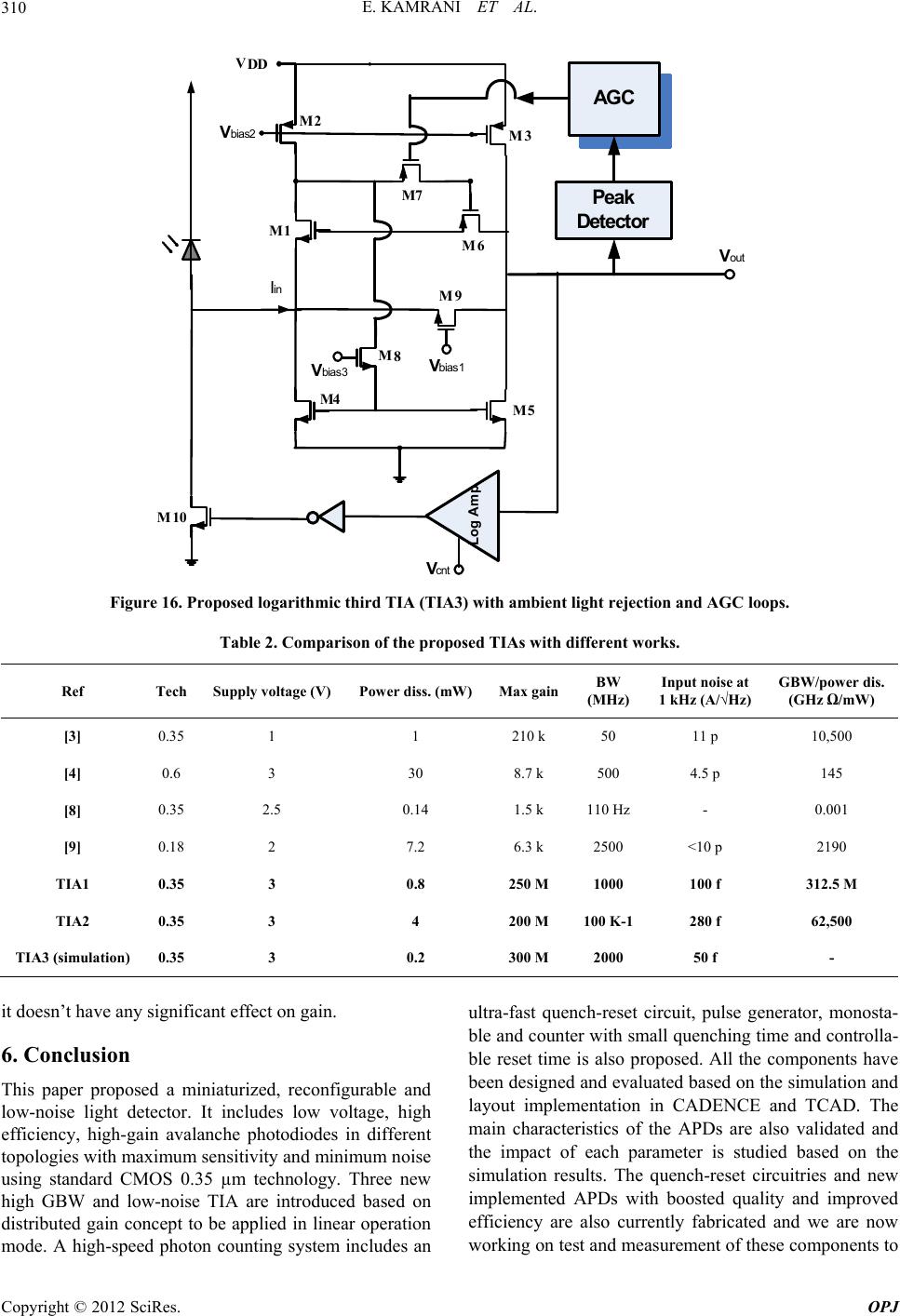 E. KAMRANI ET AL. 310 M4 M2 M1 M3 VDD M6 M7 M5 M8Vbias1 Vbias2 Vbias 3 Iin Vout Log Amp M10 M9 Vcnt AGC Peak Detector Figure 16. Proposed logarithmic third TIA (TIA3) with ambient light rejection and AGC loops. Table 2. Comparison of the proposed TIAs with different works. Ref Tech Supply voltage (V) Power diss. (mW)Max gainBW (MHz) Input noise at 1 kHz (A/√Hz) GBW/power dis. (GHz Ω/mW) [3] 0.35 1 1 210 k 50 11 p 10,500 [4] 0.6 3 30 8.7 k 500 4.5 p 145 [8] 0.35 2.5 0.14 1.5 k 110 Hz - 0.001 [9] 0.18 2 7.2 6.3 k 2500 <10 p 2190 TIA1 0.35 3 0.8 250 M 1000 100 f 312.5 M TIA2 0.35 3 4 200 M 100 K-1280 f 62,500 TIA3 (simulation) 0.35 3 0.2 300 M 2000 50 f - it doesn’t have any significant effect on gain. 6. Conclusion This paper proposed a miniaturized, reconfigurable and low-noise light detector. It includes low voltage, high efficiency, high-gain avalanche photodiodes in different topologies with maximum sensitivity and minimum noise using standard CMOS 0.35 µm technology. Three new high GBW and low-noise TIA are introduced based on distributed gain concept to be applied in linear operation mode. A high-speed photon counting system includes an ultra-fast quench-reset circuit, pulse generator, monosta- ble and counter with small quenching time and controlla- ble reset time is also proposed. All the components have been designed and evaluated based on the simulation and layout implementation in CADENCE and TCAD. The main characteristics of the APDs are also validated and the impact of each parameter is studied based on the simulation results. The quench-reset circuitries and new implemented APDs with boosted quality and improved efficiency are also currently fabricated and we are now working on test and measurement of these components to Copyright © 2012 SciRes. OPJ 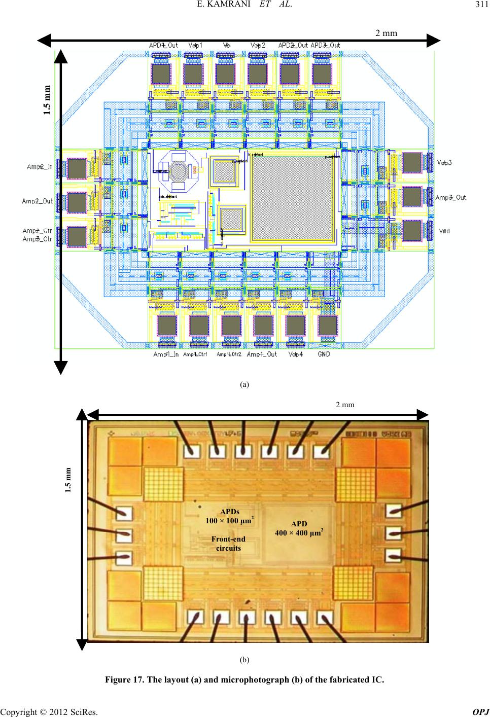 E. KAMRANI ET AL. 311 1.5 mm 2 m (a) 1.5 mm 2 mm APD 400 × 400 μm 2 Front-end circuits APDs 100 × 100 μm 2 (b) Figure 17. The layout (a) and microphotograph (b) of the fabricated IC. Copyright © 2012 SciRes. OPJ 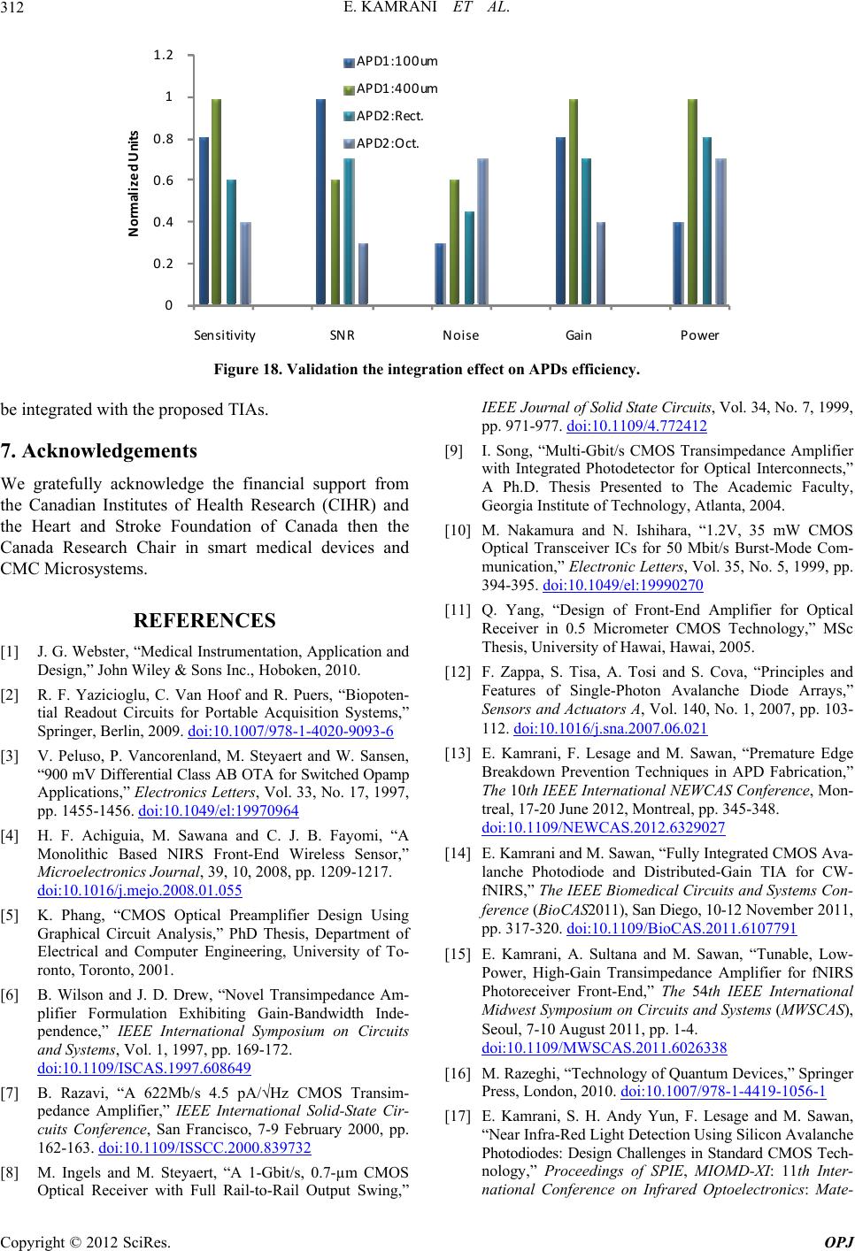 E. KAMRANI ET AL. 312 0 0.2 0.4 0.6 0.8 1 1.2 Sensitivity SNRNoiseGainPowe Normalized Units AP D1: 10 0um AP D1: 40 0um AP D2: R ect. AP D2 : Oct. Figure 18. Validation the integration effect on APDs efficiency. be integrated with the proposed TIAs. 7. Acknowledgements We gratefully acknowledge the financial support from the Canadian Institutes of Health Research (CIHR) and the Heart and Stroke Foundation of Canada then the Canada Research Chair in smart medical devices and CMC Microsystems. REFERENCES [1] J. G. Webster, “Medical Instrumentation, Application and Design,” John Wiley & Sons Inc., Hoboken, 2010. [2] R. F. Yazicioglu, C. Van Hoof and R. Puers, “Biopoten- tial Readout Circuits for Portable Acquisition Systems,” Springer, Berlin, 2009. doi:10.1007/978-1-4020-9093-6 [3] V. Peluso, P. Vancorenland, M. Steyaert and W. Sansen, “900 mV Differential Class AB OTA for Switched Opamp Applications,” Electronics Letters, Vol. 33, No. 17, 1997, pp. 1455-1456. doi:10.1049/el:19970964 [4] H. F. Achiguia, M. Sawana and C. J. B. Fayomi, “A Monolithic Based NIRS Front-End Wireless Sensor,” Microelectronics Journal, 39, 10, 2008, pp. 1209-1217. doi:10.1016/j.mejo.2008.01.055 [5] K. Phang, “CMOS Optical Preamplifier Design Using Graphical Circuit Analysis,” PhD Thesis, Department of Electrical and Computer Engineering, University of To- ronto, Toronto, 2001. [6] B. Wilson and J. D. Drew, “Novel Transimpedance Am- plifier Formulation Exhibiting Gain-Bandwidth Inde- pendence,” IEEE International Symposium on Circuits and Systems, Vol. 1, 1997, pp. 169-172. doi:10.1109/ISCAS.1997.608649 [7] B. Razavi, “A 622Mb/s 4.5 pA/√Hz CMOS Transim- pedance Amplifier,” IEEE International Solid-State Cir- cuits Conference, San Francisco, 7-9 February 2000, pp. 162-163. doi:10.1109/ISSCC.2000.839732 [8] M. Ingels and M. Steyaert, “A 1-Gbit/s, 0.7-µm CMOS Optical Receiver with Full Rail-to-Rail Output Swing,” IE EE J ournal of Solid State Ci rcuits, Vol. 34, No. 7, 1999, pp. 971-977. doi:10.1109/4.772412 [9] I. Song, “Multi-Gbit/s CMOS Transimpedance Amplifier with Integrated Photodetector for Optical Interconnects,” A Ph.D. Thesis Presented to The Academic Faculty, Georgia Institute of Technology, Atlanta, 2004. [10] M. Nakamura and N. Ishihara, “1.2V, 35 mW CMOS Optical Transceiver ICs for 50 Mbit/s Burst-Mode Com- munication,” Electronic Let ters, Vol. 35, No. 5, 1999, pp. 394-395. doi:10.1049/el:19990270 [11] Q. Yang, “Design of Front-End Amplifier for Optical Receiver in 0.5 Micrometer CMOS Technology,” MSc Thesis, University of Hawai, Hawai, 2005. [12] F. Zappa, S. Tisa, A. Tosi and S. Cova, “Principles and Features of Single-Photon Avalanche Diode Arrays,” Sensors and Actuators A, Vol. 140, No. 1, 2007, pp. 103- 112. doi:10.1016/j.sna.2007.06.021 [13] E. Kamrani, F. Lesage and M. Sawan, “Premature Edge Breakdown Prevention Techniques in APD Fabrication,” The 10th IEEE International NEWCAS Conference, Mon- treal, 17-20 June 2012, Montreal, pp. 345-348. doi:10.1109/NEWCAS.2012.6329027 [14] E. Kamrani and M. Sawan, “Fully Integrated CMOS Ava- lanche Photodiode and Distributed-Gain TIA for CW- fNIRS,” The IEEE Biomedical Circuits and Systems Con- ference (BioCAS2011), San Diego, 10-12 November 2011, pp. 317-320. doi:10.1109/BioCAS.2011.6107791 [15] E. Kamrani, A. Sultana and M. Sawan, “Tunable, Low- Power, High-Gain Transimpedance Amplifier for fNIRS Photoreceiver Front-End,” The 54th IEEE International Midwest Symposium on Circuits and Systems (MWSCAS), Seoul, 7-10 August 2011, pp. 1-4. doi:10.1109/MWSCAS.2011.6026338 [16] M. Razeghi, “Technology of Quantum Devices,” Springer Press, London, 2010. doi:10.1007/978-1-4419-1056-1 [17] E. Kamrani, S. H. Andy Yun, F. Lesage and M. Sawan, “Near Infra-Red Light Detection Using Silicon Avalanche Photodiodes: Design Challenges in Standard CMOS Tech- nology,” Proceedings of SPIE, MIOMD-XI: 11th Inter- national Conference on Infrared Optoelectronics: Mate- Copyright © 2012 SciRes. OPJ  E. KAMRANI ET AL. 313 rials and Devices, Chicago, 4-8 September 2012. [18] B. Huang, X. Zhang and H. Chen, “1 Gb/s Zero Pole Cancellation CMOS Transimpednace Amplifier for Giga- bit Ethernet Applications,” Journal of Semiconductors, Vol. 30, No. 10, 2009. [19] S. Cova, “Active Quenching Circuit for Avalanche Pho- todiodes,” US Patent 4,963,727 (Italian Patent 22367A/ 88); Licensed for Industrial Production to Silena SpA, Milano, 1990. [20] Y. Kim, I. Jun and K. H. Kim, “Design and Characteriza- tion of CMOS Avalanche Photodiode with Charge Sensi- tive Preamplifier,” IEEE Transactions on Nuclear Sci- ence, Vol. 55, No. 3, 2008, pp. 1376-1380. doi:10.1109/TNS.2008.924063 [21] E. Roncali and S. R. Cherry, “Application of Silicon Photomultipliers to Positron Emission Tomography,” An- nals of Biomedical Engineering, Vol. 39, No. 4, 2011, pp. 1358-1377. doi:10.1007/s10439-011-0266-9 [22] S. Tisa, F. Zappa, A. Tosi and S. Cova, “Electronics for Single Photon Avalanche Diode Arrays,” Sensors and Actuators A, Vol. 140, No. 1, 2007, pp. 113-122. doi:10.1016/j.sna.2007.06.022 [23] S. Tisa, A. Tosi and F. Zappa, “Fully-Integrated CMOS Single Photon Counter,” Optics Express, Vol. 15, No. 6, 2007, pp. 2873-2887. doi:10.1364/OE.15.002873 [24] V. Peluso, P. Vancorenland, M. Steyaert and W. Sansen, “900 mV Differential Class AB OTA for Switched Opamp Applications,” Electronics Letters, Vol. 33, No. 17, 1997, pp. 1455-1456. doi:10.1049/el:19970964 [25] B. Wilson and J. D. Drew, “Novel Transimpedance Am- plifier Formulation Exhibiting Gain-Bandwidth Inde- pendence,” IEEE Proceedings of International Sympo- sium on Circuits Systems, Vol. 1, 1997, pp. 169-172. [26] M. Tavakoli, L. Turicchia and R. Sarpeshkar, “An Ul- tra-Low-Power Pulse Oximeter Implemented with an En- ergy-Efficient Transimpedance Amplifier,” IEEE Trans- actions on Biomedical Circuits and Systems, Vol. 4, No. 1, 2010, pp. 27-38. doi:10.1109/TBCAS.2009.2033035 [27] T. H. Lee, “The Design of CMOS Radio-Frequency Inte- grated Circuits,” Cambridge University Press, Cambridge, 1998. doi:10.1017/CBO9780511817281 [28] R. Sarpeshkar, R. F. Lyon and C. A. Mead, “A Low- Power Wide-Dynamic-Range Analog VLSI Cochlea,” Analog Integrated Circuits and Signal Processing, Vol. 16, No. 3, 1998, pp. 245-274. doi:10.1023/A:1008218308069 [29] Q. Yang, “Design of Front-End Amplifier for Optical Receiver in 0.5 Micrometer CMOS Technology,” MSc Thesis, University of Hawai, Hawai, 2005. [30] W.-Y. Choi, M.-J. Lee and J.-S. Youn, “Si Integrated Photoreceivers,” 2010 IEEE Bipolar/BiCMOS Circuits and Technology Meeting (BCTM), Austin, 4-6 October 2010, pp. 77-81. doi:10.1109/BIPOL.2010.5667948 [31] S. Radovanovic, A.-J. Annema and B. Nauta, “A 3Gb/s Optical Detector in Standard CMOS for 850 nm Optical Communication,” IEEE Journal of Solid-State Circuits, Vol. 40, No. 8, 2005, pp. 1706-1717. doi:10.1109/JSSC.2005.852030 [32] W.-Z. Chen, S.-H. Huang, G.-W. Wu, C.-C. Liu, Y.-T. Huang, C.-F. Chiu, W.-H. Chang and Y.-Z. Juang, “A 3.125 Gbps CMOS Fully Integrated Optical Receiver with Adaptive Analog Equalizer,” Proceedings of IEEE Asian Solid-State Circuits Conference, Jeju, 12-14 No- vember 2007, pp. 396-399. doi:10.1109/ASSCC.2007.4425714 [33] F. Tavernier and M. Steyaert, “Power Efficient 4. 5 Gbit/s Optical Receiver in 130 nm CMOS with Integrated Pho- todiode,” Proceedings of European Solid-State Circuits Conference, Edinburgh, 15-19 September 2008, pp. 162- 165. [34] W.-Z. Chen and S.-H. Huang, “A 2.5 Gbps CMOS Fully Integrated Optical Receiver with Lateral PIN Detector,” Proceedings of Custom Integrated Circuits Conference, San Jose, 16-19 September 2007, pp. 293-296. doi:10.1109/CICC.2007.4405736 [35] J.-S. Youn, H.-S. Kang, M.-J. Lee, K.-Y. Park and W.-Y. Choi, “High-Speed CMOS Integrated Optical Receiver with an Avalanche Photodetector,” IEEE Photonics Tech- nology Letters, Vol. 21, No. 20, 2009, pp. 1553-1555. doi:10.1109/LPT.2009.2029869 [36] A. Sultana, E. Kamrani and M. Sawan, “CMOS Silicon Avalanche Photodiodes for NIR Light Detection: A Sur- vey,” Journal of Analog Integrated Circuits and Signal Processing, 2012, pp. 1-13. doi:10.1007/s10470-011-9641-6 [37] J.-S. Youn, M.-J. Lee, K.-Y. Park, H. Rücker and W.-Y. Choi, “7-Gb/s Monolithic Photoreceiver Fabricated with 0.25-μm SiGe BiCMOS Technology,” IEICE Electronics Express, Vol. 7, No. 9, 2010, pp. 659-665. doi:10.1587/elex.7.659 [38] E. Kamrani, S. H. A. Yun, F. Lesage and M. Sawan, “State-of-the-Art Logarithmic Transimpedance Amplifier with Automatic Gain Control and Ambient Light Rejec- tion for fNIRS,” Proceedings of SPIE MIOMD-XI, Chi- cago, 4-8 September 2012, pp. 58-59. [39] E. Kamrani, S. H. Andy Yun, F. Lesage and M. Sawan, “Optimal-Adaptive Control System for Low-Noise, Low- Power and Fast Photodetection in Functional Near Infra- Red Spectroscopy,” Proceedings of SPIE, MIOMD-XI, Chicago, 4-8 September 2012. Copyright © 2012 SciRes. OPJ
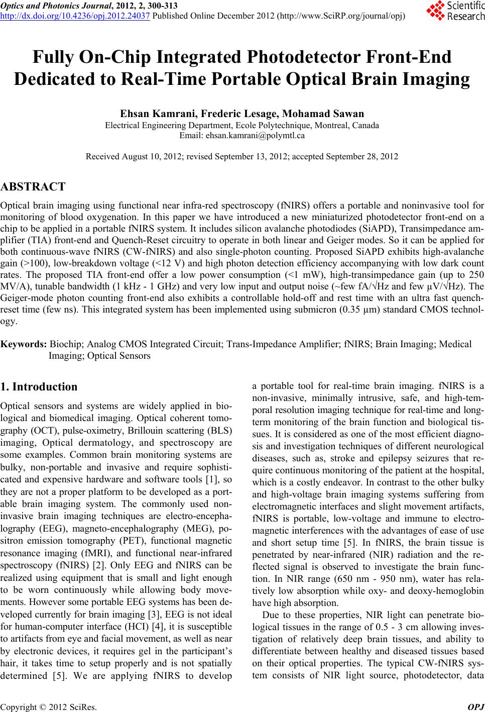
|