Paper Menu >>
Journal Menu >>
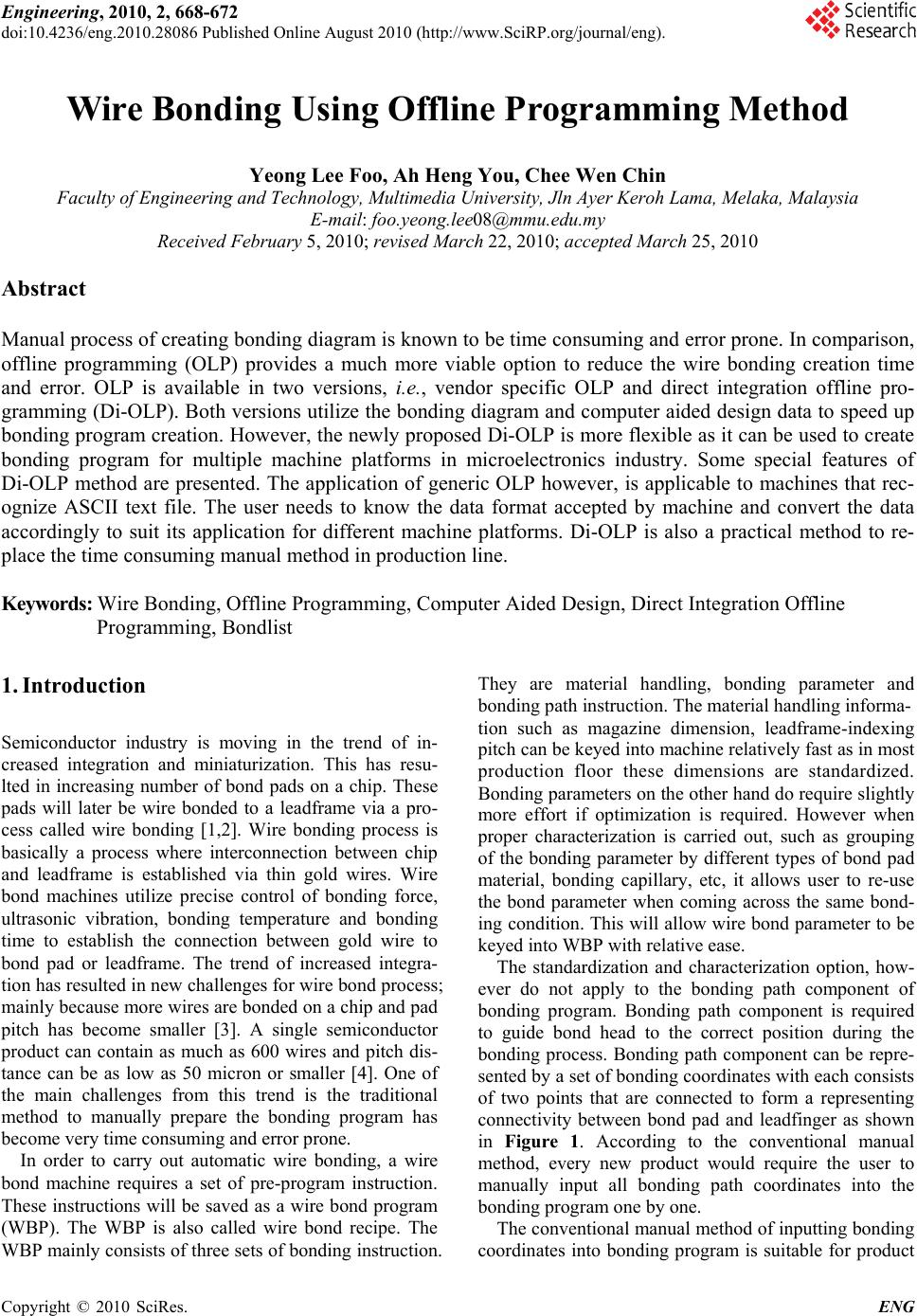 Engineering, 2010, 2, 668-672 doi:10.4236/eng.2010.28086 Published Online August 2010 (http://www.SciRP.org/journal/eng). Copyright © 2010 SciRes. ENG Wire Bonding Using Offline Programming Method Yeong Lee Foo, Ah Heng You, Chee Wen Chin Faculty of Engineering and Technology, Multimedia University, Jln Ayer Keroh Lama, Melaka, Malaysia E-mail: foo.yeong.lee08@mmu.edu.my Received February 5, 2010; revised March 22, 2010; accepted March 25, 2010 Abstract Manual process of creating bonding diagram is known to be time consuming and error prone. In comparison, offline programming (OLP) provides a much more viable option to reduce the wire bonding creation time and error. OLP is available in two versions, i.e., vendor specific OLP and direct integration offline pro- gramming (Di-OLP). Both versions utilize the bonding diagram and computer aided design data to speed up bonding program creation. However, the newly proposed Di-OLP is more flexible as it can be used to create bonding program for multiple machine platforms in microelectronics industry. Some special features of Di-OLP method are presented. The application of generic OLP however, is applicable to machines that rec- ognize ASCII text file. The user needs to know the data format accepted by machine and convert the data accordingly to suit its application for different machine platforms. Di-OLP is also a practical method to re- place the time consuming manual method in production line. Keywords: Wire Bonding, Offline Programming, Computer Aided Design, Direct Integration Offline Programming, Bondlist 1. Introduction Semiconductor industry is moving in the trend of in- creased integration and miniaturization. This has resu- lted in increasing number of bond pads on a chip. These pads will later be wire bonded to a leadframe via a pro- cess called wire bonding [1,2]. Wire bonding process is basically a process where interconnection between chip and leadframe is established via thin gold wires. Wire bond machines utilize precise control of bonding force, ultrasonic vibration, bonding temperature and bonding time to establish the connection between gold wire to bond pad or leadframe. The trend of increased integra- tion has resulted in new challenges for wire bond process; mainly because more wires are bonded on a chip and pad pitch has become smaller [3]. A single semiconductor product can contain as much as 600 wires and pitch dis- tance can be as low as 50 micron or smaller [4]. One of the main challenges from this trend is the traditional method to manually prepare the bonding program has become very time consuming and error prone. In order to carry out automatic wire bonding, a wire bond machine requires a set of pre-program instruction. These instructions will be saved as a wire bond program (WBP). The WBP is also called wire bond recipe. The WBP mainly consists of three sets of bonding instruction. They are material handling, bonding parameter and bonding path instruction. The material handling informa- tion such as magazine dimension, leadframe-indexing pitch can be keyed into machine relatively fast as in most production floor these dimensions are standardized. Bonding parameters on the other hand do require slightly more effort if optimization is required. However when proper characterization is carried out, such as grouping of the bonding parameter by different types of bond pad material, bonding capillary, etc, it allows user to re-use the bond parameter when coming across the same bond- ing condition. This will allow wire bond parameter to be keyed into WBP with relative ease. The standardization and characterization option, how- ever do not apply to the bonding path component of bonding program. Bonding path component is required to guide bond head to the correct position during the bonding process. Bonding path component can be repre- sented by a set of bonding coordinates with each consists of two points that are connected to form a representing connectivity between bond pad and leadfinger as shown in Figure 1. According to the conventional manual method, every new product would require the user to manually input all bonding path coordinates into the bonding program one by one. The conventional manual method of inputting bonding coordinates into bonding program is suitable for product 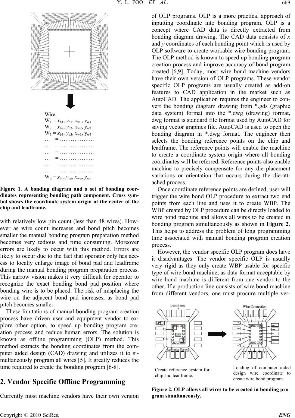 Y. L. FOO ET AL. Copyright © 2010 SciRes. ENG 669 Wire, W 1 = x b1 , y b1 , x w1 , y w1 W 2 = x b2 , y b2 , x w2 , y w2 W 3 = x b3 , y b3 , x w3 , y w3 … = ………………. … = ………………. … = ………………. … = ………………. … = ………………. … = ………………. W n = x bn , y bn , x wn , y wn Figure 1. A bonding diagram and a set of bonding coor- dinates representing bonding path component. Cross sym- bol shows the coordinate system origin at the center of the chip and leadframe. with relatively low pin count (less than 48 wires). How- ever as wire count increases and bond pitch becomes smaller the manual bonding program preparation method becomes very tedious and time consuming. Moreover errors are likely to occur with this method. Errors are likely to occur due to the fact that operator only has acc- ess to locally enlarge image of bond pad and leadframe during the manual bonding program preparation process. This narrow vision makes it very difficult for operator to recognize the exact bonding bond pad position where bonding wire is to be placed. The risk of misplacing the wire on the adjacent bond pad increases, as bond pad pitch becomes smaller. These limitations of manual bonding program creation process have driven user and equipment vendor to ex- plore other option, to speed up bonding program cre- ation process and reduce human errors. The solution is known as offline programming (OLP) method. This method extracts the bonding coordinates from the com- puter aided design (CAD) drawing and utilizes it to si- multaneously program all wires [5]. It greatly reduces the time required to create the bonding program [6-8]. 2. Vendor Specific Offline Programming Currently most machine vendors have their own version of OLP programs. OLP is a more practical approach of inputting coordinate into bonding program. OLP is a concept where CAD data is directly extracted from bonding diagram drawing. The CAD data consists of x and y coordinates of each bonding point which is used by OLP software to create workable wire bonding program. The OLP method is known to speed up bonding program creation process and improve accuracy of bond program created [6,9]. Today, most wire bond machine vendors have their own version of OLP programs. These vendor specific OLP programs are usually created as add-on features to CAD application in the market such as AutoCAD. The application requires the engineer to con- vert the bonding diagram drawing from *.gds (graphic data system) format into the *.dwg (drawing) format, dwg format is standard file format used by AutoCAD for saving vector graphics file. AutoCAD is used to open the bonding diagram in *.dwg format. The engineer then selects the bonding reference points on the chip and leadframe. The reference points will enable the machine to create a coordinate system origin where all bonding coordinates will be referred. Reference points also enable machine to precisely compensate for any die placement variations or orientation that occurs during the die-att- ached process. Once coordinate reference points are defined, user will trigger the wire bond OLP procedure to extract two end points from each line and uses it to create WBP. The WBP created by OLP procedure can be directly loaded to wire bond machine and allows all wires to be created in bonding program simultaneously as shown in Figure 2. This helps to address the problem of long programming time associated with manual bonding program creation process. However, the vendor specific OLP program does have it disadvantages. The vendor specific OLP is usually very rigid as they only create WBP usable for specific type of wire bond machine, as data format acceptable by wire bond machine is different from one vendor to the other. If a production line consists of wire bond machine from different vendors, one must procure multiple ver- Figure 2. OLP allows all wires to be created in bonding pro- gram simultaneously. Create reference system for chip and leadframe. Loading of computer aided design wire coordinate to create wire bond program. 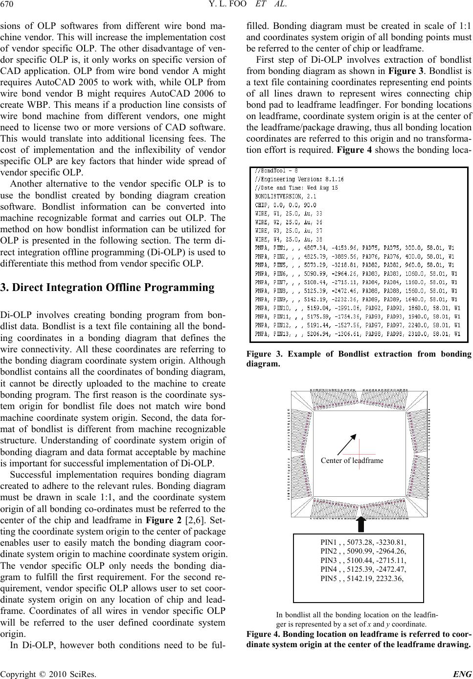 Y. L. FOO ET AL. Copyright © 2010 SciRes. ENG 670 sions of OLP softwares from different wire bond ma- chine vendor. This will increase the implementation cost of vendor specific OLP. The other disadvantage of ven- dor specific OLP is, it only works on specific version of CAD application. OLP from wire bond vendor A might requires AutoCAD 2005 to work with, while OLP from wire bond vendor B might requires AutoCAD 2006 to create WBP. This means if a production line consists of wire bond machine from different vendors, one might need to license two or more versions of CAD software. This would translate into additional licensing fees. The cost of implementation and the inflexibility of vendor specific OLP are key factors that hinder wide spread of vendor specific OLP. Another alternative to the vendor specific OLP is to use the bondlist created by bonding diagram creation software. Bondlist information can be converted into machine recognizable format and carries out OLP. The method on how bondlist information can be utilized for OLP is presented in the following section. The term di- rect integration offline programming (Di-OLP) is used to differentiate this method from vendor specific OLP. 3. Direct Integration Offline Programming Di-OLP involves creating bonding program from bon- dlist data. Bondlist is a text file containing all the bond- ing coordinates in a bonding diagram that defines the wire connectivity. All these coordinates are referring to the bonding diagram coordinate system origin. Although bondlist contains all the coordinates of bonding diagram, it cannot be directly uploaded to the machine to create bonding program. The first reason is the coordinate sys- tem origin for bondlist file does not match wire bond machine coordinate system origin. Second, the data for- mat of bondlist is different from machine recognizable structure. Understanding of coordinate system origin of bonding diagram and data format acceptable by machine is important for successful implementation of Di-OLP. Successful implementation requires bonding diagram created to adhere to the relevant rules. Bonding diagram must be drawn in scale 1:1, and the coordinate system origin of all bonding co-ordinates must be referred to the center of the chip and leadframe in Figure 2 [2,6]. Set- ting the coordinate system origin to the center of package enables user to easily match the bonding diagram coor- dinate system origin to machine coordinate system origin. The vendor specific OLP only needs the bonding dia- gram to fulfill the first requirement. For the second re- quirement, vendor specific OLP allows user to set coor- dinate system origin on any location of chip and lead- frame. Coordinates of all wires in vendor specific OLP will be referred to the user defined coordinate system origin. In Di-OLP, however both conditions need to be ful- filled. Bonding diagram must be created in scale of 1:1 and coordinates system origin of all bonding points must be referred to the center of chip or leadframe. First step of Di-OLP involves extraction of bondlist from bonding diagram as shown in Figure 3. Bondlist is a text file containing coordinates representing end points of all lines drawn to represent wires connecting chip bond pad to leadframe leadfinger. For bonding locations on leadframe, coordinate system origin is at the center of the leadframe/package drawing, thus all bonding location coordinates are referred to this origin and no transforma- tion effort is required. Figure 4 shows the bonding loca- Figure 3. Example of Bondlist extraction from bonding diagram. Figure 4. Bonding location on leadframe is referred to coor- dinate system origin at the center of the leadframe drawing. Center of leadframe PIN1 , , 5073.28, -3230.81, PIN2 , , 5090.99, -2964.26, PIN3 , , 5100.44, -2715.11, PIN4 , , 5125.39, -2472.47, PIN5 , , 5142.19, 2232.36, In bondlist all the bonding location on the leadfin- ger is represented by a set of x and y coordinate. 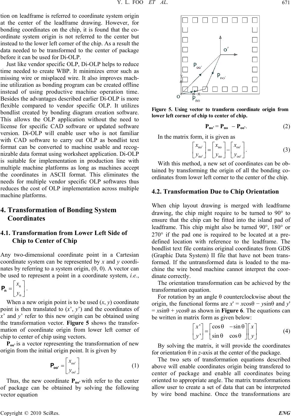 Y. L. FOO ET AL. Copyright © 2010 SciRes. ENG 671 tion on leadframe is referred to coordinate system origin at the center of the leadframe drawing. However, for bonding coordinates on the chip, it is found that the co- ordinate system origin is not referred to the center but instead to the lower left corner of the chip. As a result the data needed to be transformed to the center of package before it can be used for Di-OLP. Just like vendor specific OLP, Di-OLP helps to reduce time needed to create WBP. It minimizes error such as missing wire or misplaced wire. It also improves mach- ine utilization as bonding program can be created offline instead of using productive machine operation time. Besides the advantages described earlier Di-OLP is more flexible compared to vendor specific OLP. It utilizes bondlist created by bonding diagram creation software. This allows the OLP application without the need to license for specific CAD software or updated software version. Di-OLP will enable user who is not familiar with CAD software to carry out OLP as bondlist text format can be converted to machine usable and recog- nizable data format using worksheet application. Di-OLP is suitable for implementation in production line with multiple machine platforms as long as machines accept the coordinates in ASCII format. This eliminates the needs for multiple vendor specific OLP softwares thus reduces the cost of OLP implementation across multiple machine platforms. 4. Transformation of Bonding System Coordinates 4.1. Transformation from Lower Left Side of Chip to Center of Chip Any two-dimensional coordinate point in a Cartesian coordinate system can be represented by x and y coordi- nates by referring to a system origin, (0, 0). A vector can be used to represent a point in a coordinate system, i.e., n n x y n P. When a new origin point is to be used (x, y) coordinate point is then translated to (x’, y’) and the coordinates of x’ and y’ refer to this new origin can be obtained using the transformation vector. Figure 5 shows the transfor- mation of coordinate origin from lower left corner of chip to center of chip using vectors. Poo’ is a vector representing the transformation of new origin from the initial origin point. It is given by oo' oo' x y oo' P (1) Thus, the new coordinate Pno’ with refer to the center of package can be obtained by solving the following vector equation Figure 5. Using vector to transform coordinate origin from lower left corner of chip to center of chip. Pno’ = Pno Poo’. (2) In the matrix form, it is given as no'no oo' no'no oo' x xx yyy . (3) With this method, a new set of coordinates can be ob- tained by transforming the origin of all the bonding co- ordinates from lower left corner to the center of the chip. 4.2. Transformation Due to Chip Orientation When chip layout drawing is merged with leadframe drawing, the chip might require to be turned to 90 to ensure that the chip can be fitted into the island pad of leadframe. This chip might also be turned 90, 180 or 270 if the pad one is required to be located at a pre- defined location with reference to the leadframe. The bondlist text file contains original coordinates from GDS (Graphic Data System) II file that have not been trans- formed. If the untransformed data is loaded to the ma- chine the wire bond machine cannot interpret the coor- dinate correctly. The orientation transformation can be achieved by the transformation equation. For rotation by an angle θ counterclockwise about the origin, the functional forms are x' = xcosθ − ysinθ and y' = xsinθ + ycosθ as shown in Figure 6. The equations can be written in matrix form as given below: 'cos 'sin x y sin cos x y (4) By solving the matrix, it will provide the coordinates for orientation θ in z-axis at the center of the package. The two sets of transformation equations described above will enable coordinates origin being transfered to center of package and enable all coordinates being oriented to appropriate angle. The matrix transformations allow user to create a set of data that can be interpreted by wire bond machine. Once the transformations are 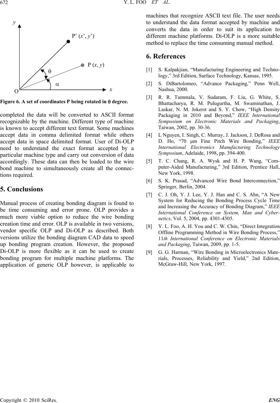 Y. L. FOO ET AL. Copyright © 2010 SciRes. ENG 672 Figure 6. A set of coordinates P being rotated in degree. completed the data will be converted to ASCII format recognizable by the machine. Different type of machine is known to accept different text format. Some machines accept data in comma delimited format while others accept data in space delimited format. User of Di-OLP need to understand the exact format accepted by a particular machine type and carry out conversion of data accordingly. These data can then be loaded to the wire bond machine to simultaneously create all the connec- tions required. 5. Conclusions Manual process of creating bonding diagram is found to be time consuming and error prone. OLP provides a much more viable option to reduce the wire bonding creation time and error. OLP is available in two versions, vendor specific OLP and Di-OLP as described. Both versions utilize the bonding diagram CAD data to speed up bonding program creation. However, the proposed Di-OLP is more flexible as it can be used to create bonding program for multiple machine platforms. The application of generic OLP however, is applicable to machines that recognize ASCII text file. The user needs to understand the data format accepted by machine and converts the data in order to suit its application to different machine platforms. Di-OLP is a more suitable method to replace the time consuming manual method. 6. References [1] S. Kalpakjian, “Manufacturing Engineering and Techno- logy,” 3rd Edition, Surface Technology, Kansas, 1995. [2] S. DiBartolomeo, “Advance Packaging,” Penn Well, Nashua, 2000. [3] R. R. Tummala, V. Sudaram, F. Liu, G. White, S. Bhattacharya, R. M. Pulugurtha, M. Swaminathan, J. Laskar, N. M. Jokerst and S. Y. Chow, “High Density Packaging in 2010 and Beyond,” IEEE International Symposium on Electronic Materials and Packaging, Taiwan, 2002, pp. 30-36. [4] L Nguyen, I. Singh, C. Murray, J. Jackson, J. DeRosa and D. Ho, “70 μm Fine Pitch Wire Bonding,” IEEE International Electronics Manufacturing Technology Symposium, Adelaide, 1998, pp. 394-400. [5] T. C. Chang, R. A. Wysk and H. P. Wang, “Com- puter-Aided Manufacturing,” 3rd Edition, Prentice Hall, New York, 1998. [6] S. K. Prasad, “Advanced Wire Bond Interconnection,” Springer, Berlin, 2004. [7] C. J. Oh, Y. J. Lee, Y. J. Han and C. S. Ahn, “A New System for Reducing the Bonding Process Cycle Time and Increasing the Accuracy of Bonding Diagram,” IEEE International Conference on System, Man and Cyber- netics, Vol. 5, 2004, pp. 4301-4305. [8] Y. L. Foo, A. H. You and C. W. Chin, “Direct Integration Offline Programming Method in Wire Bonding Process,” 11th International Conference on Electronic Materials and Packaging, Taiwan, 2009, pp. 1-5. [9] G. G. Harman, “Wire Bonding in Microelectronics Mate- rials, Processes, Reliability and Yield,” 2nd Edition, McGraw-Hill, New York, 1997. y x P (x, y) P’ (x’, y’) O |