Paper Menu >>
Journal Menu >>
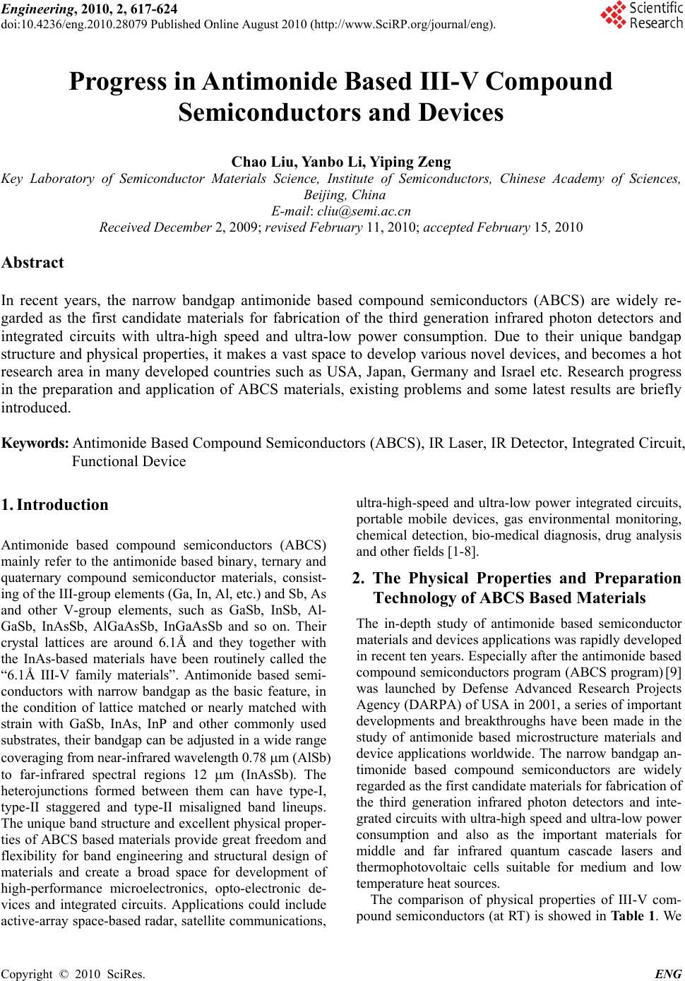 Engineering, 2010, 2, 617-624 doi:10.4236/eng.2010.28079 Published Online August 2010 (http://www.SciRP.org/journal/eng). Copyright © 2010 SciRes. ENG Progress in Antimonide Based III-V Compound Semiconductors and Devices Chao Liu, Yanbo Li, Yiping Zeng Key Laboratory of Semiconductor Materials Science, Institute of Semiconductors, Chinese Academy of Sciences, Beijing, China E-mail: cliu@semi.ac.cn Received December 2, 2009; revised February 11, 2010; accepted February 15, 2010 Abstract In recent years, the narrow bandgap antimonide based compound semiconductors (ABCS) are widely re- garded as the first candidate materials for fabrication of the third generation infrared photon detectors and integrated circuits with ultra-high speed and ultra-low power consumption. Due to their unique bandgap structure and physical properties, it makes a vast space to develop various novel devices, and becomes a hot research area in many developed countries such as USA, Japan, Germany and Israel etc. Research progress in the preparation and application of ABCS materials, existing problems and some latest results are briefly introduced. Keywords: Antimonide Based Compound Semiconductors (ABCS), IR Laser, IR Detector, Integrated Circuit, Functional Device 1. Introduction Antimonide based compound semiconductors (ABCS) mainly refer to the antimonide based binary, ternary and quaternary compound semiconductor materials, consist- ing of the III-group elements (Ga, In, Al, etc.) and Sb, As and other V-group elements, such as GaSb, InSb, Al- GaSb, InAsSb, AlGaAsSb, InGaAsSb and so on. Their crystal lattices are around 6.1Å and they together with the InAs-based materials have been routinely called the “6.1Å III-V family materials”. Antimonide based semi- conductors with narrow bandgap as the basic feature, in the condition of lattice matched or nearly matched with strain with GaSb, InAs, InP and other commonly used substrates, their bandgap can be adjusted in a wide range coveraging from near-infrared wavelength 0.78 m (AlSb) to far-infrared spectral regions 12 m (InAsSb). The heterojunctions formed between them can have type-I, type-II staggered and type-II misaligned band lineups. The unique band structure and excellent physical proper- ties of ABCS based materials provide great freedom and flexibility for band engineering and structural design of materials and create a broad space for development of high-performance microelectronics, opto-electronic de- vices and integrated circuits. Applications could include active-array space-based radar, satellite communications, ultra-high-speed and ultra-low power integrated circuits, portable mobile devices, gas environmental monitoring, chemical detection, bio-medical diagnosis, drug analysis and other fields [1-8]. 2. The Physical Properties and Preparation Technology of ABCS Based Materials The in-depth study of antimonide based semiconductor materials and devices applications was rapidly developed in recent ten years. Especially after the antimonide based compound semiconductors program (ABCS program) [9] was launched by Defense Advanced Research Projects Agency (DARPA) of USA in 2001, a series of important developments and breakthroughs have been made in the study of antimonide based microstructure materials and device applications worldwide. The narrow bandgap an- timonide based compound semiconductors are widely regarded as the first candidate materials for fabrication of the third generation infrared photon detectors and inte- grated circuits with ultra-high speed and ultra-low power consumption and also as the important materials for middle and far infrared quantum cascade lasers and thermophotovoltaic cells suitable for medium and low temperature heat sources. The comparison of physical properties of III-V com- pound semiconductors (at RT) is showed in Table 1. We 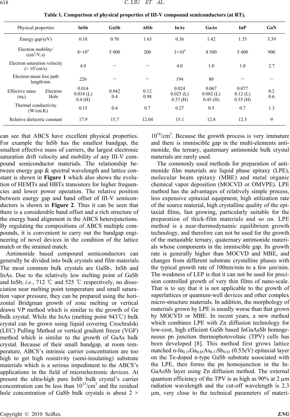 C. LIU ET AL. Copyright © 2010 SciRes. ENG 618 Table 1. Comparison of physical properties of III-V compound semiconductors (at RT). Physical properties InSb GaSb AlSb InAs GaAs InP GaN Energy gap/(eV) 0.18 0.70 1.63 0.36 1.42 1.35 3.39 Electron mobility/ (cm2/V.s) 8×10⁴ 5 000 200 3×10⁴ 8 500 5 400 900 Electron saturation velocity (× 107cm/s) 4.0 - - 4.0 1.0 1.0 2.7 Electron mean free path length/nm 226 - - 194 80 - - Effective mass (m0) Electron Hole 0.014 0.018 (L) 0.4 (H) 0.042 0.4 0.12 0.98 0.024 0.025 (L) 0.37 (H) 0.067 0.082 (L) 0.45 (H) 0.077 0.12 (L) 0.55 (H) 0.2 0.6 Thermal conductivity (W/cm.K) 0.15 0.4 0.7 0.27 0.5 0.7 1.3 Relative dielectric constant 17.9 15.7 12.04 15.1 12.8 12.5 9 can see that ABCS have excellent physical properties. For example the InSb has the smallest bandgap, the smallest effective mass of carriers, the largest electronic saturation drift velocity and mobility of any III-V com- pound semiconductor materials. The relationship be- tween energy gap & spectral wavelength and lattice con- stant is shown in Figure 1 which also shows the evolu- tion of HEMTs and HBTs transistors for higher frequen- cies and lower power operation. The relative position between energy gap and band offset of III-V semicon- ductors is shown in Figure 2. Thus it can be seen that there is a considerable band offset and a rich structure of the energy band alignment in the ABCS heterojunctions. By regulating the compositions of ABCS multiple com- pounds, it is convenient to carry out the bandgap engi- neering of novel devices in the condition of the lattice match or the strained match. Antimonide based compound semiconductors can generally be divided into bulk crystals and film materials. The most common bulk crystals are GaSb、InSb and InAs. Due to the relatively low melting point of GaSb and InSb, i.e., 712 and 525 respectively, no diss℃℃ o- ciation near melting point temperature and small satura- tion vapor pressure, they can be prepared using the hori- zontal Bridgman growth of zone melting or vertical drawn VP method which is similar to the growth of Ge bulk crystal. While the InAs (melting point 943) bulk ℃ crystal can be grown using liquid covering Czochralski (LEC) Pulling Method or vertical gradient freeze (VGF) method which is similar to the growth of GaAs bulk crystal. Because of their small bandgap, at room tem- perature, ABCS’s intrinsic carrier concentration are too high to get high resistivity (semi-insulating) substrate materials which is a serious impediment to the ABCS’s applications in the field of microelectronic devices. At present the ultra-high pure InSb bulk crystal’s carrier concentration can be less than 1013/cm3 and the residual hole concentration of GaSb bulk crystals is about 2 × 10¹⁶/cm3. Because the growth process is very immature and there is immiscible gap in the multi-elements anti- monide, the ternary, quaternary antimonide bulk crystal materials are rarely used. The commonly used methods for preparation of anti- monide film materials are liquid phase epitaxy (LPE), molecular beam epitaxy (MBE) and metal organic chemical vapor deposition (MOCVD or OMVPE). LPE method has the advantages of relatively simple process, less expensive epitaxial equipment, high utilization rate of the source material, high crystalline quality of the epi- taxial films, fast growing, particularly suitable for the preparation of thick-film materials and so on. LPE method is a near-thermodynamic equilibrium growth technology, and therefore can not be used for the growth of the metastable ternary, quaternary antimonide materi- als whose components in the immiscible gap. Its growth rate is generally higher than MOCVD and MBE, and changes from different substrate crystalline phases with the typical growth rate of 100nm/min to a few μm/min. The weakness of LEP is that it can not be used for preci- sion controlled growth of very thin films of nano-scale. That is to say that it is not applicable to the growth of superlattices or quantum-well devices and other complex micro-structure materials. In addition, the morphology of materials grown by LPE is usually worse than that grown by MOCVD or MBE. In recent years, a new method which combines LPE with Zn diffusion technology for low-cost, high efficient GaSb based InGaAsSb homoge- neous pn junction thermophotovoltaic (TPV) cells has been developed [8]. This method first grows lattice matched n-In0.15Ga0.85As0.17Sb0.83 (0.55eV) epitaxial layer on the Te-doped n-type GaSb substrate associated with the LPE, then forms the pn homojunction in the In- GaAsSb layer using Zn diffusion method. The external quantum efficiency of the TPV is as high as 90% at 2 m radiation wavelength and the cut-off wavelength is 2.3 m, very close to the technical parameters of materi- 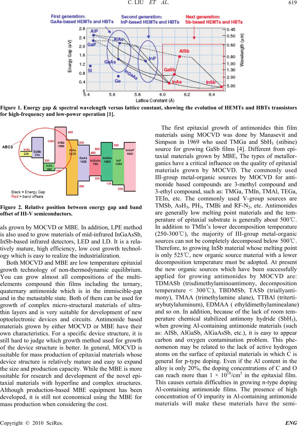 C. LIU ET AL. Copyright © 2010 SciRes. ENG 619 Figure 1. Energy gap & spectral wavelength versus lattice constant, showing the evolution of HEMTs and HBTs transistors for high-frequency and low-power operation [1]. Figure 2. Relative position between energy gap and band offset of III-V semiconductors. als grown by MOCVD or MBE. In addition, LPE method is also used to grow materials of mid-infrared InGaAsSb, InSb-based infrared detectors, LED and LD. It is a rela- tively mature, high efficiency, low cost growth technol- ogy which is easy to realize the industrialization. Both MOCVD and MBE are low temperature epitaxial growth technology of non-thermodynamic equilibrium. You can grow almost all compositions of the multi- elements compound thin films including the ternary, quaternary antimonide which is in the immiscible-gap and in the metastable state. Both of them can be used for growth of complex micro-structural materials of ultra- thin layers and is very suitable for development of new optoelectronic devices and circuits. Antimonide based materials grown by either MOCVD or MBE have their own characteristics. For a specific device structure, it is still hard to judge which growth method used for growth of the device structure is better. In general, MOCVD is suitable for mass production of epitaxial materials whose device structure is relatively mature and easy to expand the size and production capacity. While the MBE is more suitable for research and development of the novel epi- taxial materials with hyperfine and complex structures. Although production-based MBE equipment has been developed, it is still not economical using the MBE for mass production when considering the cost. The first epitaxial growth of antimonides thin film materials using MOCVD was done by Manasevit and Simpson in 1969 who used TMGa and SbH3 (stibine) source for growing GaSb films [4]. Different from epi- taxial materials grown by MBE, The types of metallor- ganics have a critical influence on the quality of epitaxial materials grown by MOCVD. The commonly used III-group metal-organic sources by MOCVD for anti- monide based compounds are 3-methyl compound and 3-ethyl compound, such as: TMGa, TMIn, TMAl, TEGa, TEIn, etc. The commonly used V-group sources are TMSb, AsH3, PH3, TMBi and RF-N2, etc. Antimonides are generally low melting point materials and the tem- perature of epitaxial substrate is generally about 500. ℃ In addition to TMIn’s lower decomposition temperature (250-300), the majority of III℃-group metal-organic sources can not be completely decomposed below 500. ℃ Therefore, to growing InSb material whose melting point is only 525, new organic source material with a lower ℃ decomposition temperature must be adopted. At present the new organic sources which have been successfully applied for growing antimonides by MOCVD are: TDMASb (trisdimethylaminoantimony, decomposition temperature < 300), TBDMSb, TASb (triallyant℃i- mony), TMAA (trimethylamine alane), TTBAl (triterti- arybutylaluminum), EDMAA ( ethyldimethylaminealane) and so on. In addition, because of the lack of room tem- perature chemical stabilized antimony hydride (SbH3), when growing Al-containing antimonide materials (such as: AlSb, AlGaSb, AlGaAsSb, etc.), it is easy to appear carbon and oxygen contamination problem. This phe- nomenon may be related to the lack of active hydrogen atoms on the surface of epitaxial materials in which C is general for p-type doping. Even if the Al content in the alloy is only 20%, the doping concentrations of C and O can reach more than 1 × 10¹⁸/cm3 in the epitaxial film. This causes certain difficulties in growing n-type doping Al-containing antimonide films. The presence of high concentration of O impurity in Al-containing antimonide materials will make these materials have the semi-  C. LIU ET AL. Copyright © 2010 SciRes. ENG 620 insulating properties and difficult to measure their elec- trical properties. The origin of O impurity is very com- plex, and both the purity of the metal organic sources and the epitaxial environment and process conditions are closely related. The development of new organic alumi- num source such as TMAA, TTBAl, EDMAA etc. is precisely in order to inhibit the serious C contamination problem [4-5]. Thus, growing AlSb and their multiele- ment materials using MOCVD is the most challenging work in all the III-V epitaxial materials technologies. The epitaxial growth of antimonide materials using MBE was following earlier pioneering work of the IBM group of L.L Chang and L. Esak, first on InAs/GaSb and InAs/AlSb films [3]. Different from MOCVD process, MBE uses ultra-high vacuum epitaxial environment with single-element materials for molecular beam sources and is easy to implement epitaxy of atomic layer and in situ real-time monitoring, avoiding the C-pollution problem which exits in Al-containing materials growing by MOCVD and greatly reducing the concentration of O doping. In fact most of the prototype devices having complex fine structures and low-dimensional structures (quantum wells, quantum wires and quantum dots) were first achieved using materials grown by MBE. It is noteworthy that, no matter MOCVD or MBE method, the use of substrates whose surface orientation have a small angle offset (i.e., low-density atomic step on the surface of the substrate) seem to be more accessible high-quality epitaxial layers. Experiments confirmed that the use of GaSb (100) substrates miscut 2° towards (110) or 6° towards (1ī1) B may get higher crystal quality of InGaAsSb and AlGaAsSb epitaxial layers [5]. To over- come the difficulty that antimonides have no semi-insu- lating substrate materials, the use of GaAs, Si and other heterogeneous substrate materials for epitaxy of ABCS films have also attracted great attention. H. Toyota, etc. [10] reported that they grown high-quality GaSb/AlGaSb multi-quantum well (MQW) structures with a 5nm AlSb initiation layer and a relatively thick GaSb buffer layer (0.5-2.0 µm) grown on Si (001) substrates by molecular beam epitaxy. The photoluminescence (PL) emission around 1.55 µm wavelength was observed for GaSb/ AlGaSb MQW structure at room temperature. Low dis- location density, high-quality GaSb epitaxial films on GaAs (001) substrates stripe-patterned with SiO2 is also prepared by MOCVD with low temperature epitaxial lateral overgrowth (ELO) method [11]. Apart from common binary, ternary and quaternary antimonides being composed of Al, Ga, In, As and Sb, in order to extend the applications of antimonide-based materials in the far-infrared band ( 5 m), easy to adjust the material lattice constant to match the substrates’ lat- tice constant of GaSb, InAs et al. and develop new func- tional materials, recently some ternary, quaternary anti- monides containing N( 2%), P or Bi( 2%) and five- elements antimonides such as AlGaInAsSb, GaInNAsSb etc have also aroused people’s concern and research in- terest [12-14]. T. Ashlet, etc. [12] found that the addition of a small percentage of nitrogen ( 2%) to GaSb, InSb, and GaInSb materials would significantly change their energy band structures (bandgap become smaller) which is very conducive to develop multi-band infrared detec- tors. 3. Application of ABCS Materials The early focus of antimonide based compound semi- conductors comes from its application prospect in mid- and far-infrared (photon) detectors, but the first to enter the market and get a large-scale industrial production is high-sensitivity InSb magnetoresistive Hall sensors. In 2004, Asahi Kasei Electronic (AKE) of Japan which ac- count for 70% of the global market share of Hall sensors announced that its InSb Hall sensor output had reached more than 100 million per month. These products are widely used in small brushless DC motors, automotive electronics and consumer electronics products and other fields. InSb-based infrared detector arrays have gained a market dominant position of ground-infrared applications and space instrumentation fields. In addition to these more mature products, antimonide materials have made great progress in the third-generation infrared focal plane array detectors, mid and far infrared quantum cascade lasers, quantum dot lasers, ultra-high-speed, ultra-low- power and low-noise amplifiers, thermophotovoltaic devices and so on in recent years. The following de- scribes some latest results and trends of development of application of ABSC materials. 3.1. Microelectronic Devices and Integrated Circuits HEMT and HBT devices and circuits used by millime- ter-wave radar and high-frequency digital communica- tions have so far experienced first generation based on GaAs-based materials, second generation based on InP-based materials and is currently to the development of third generation of HEMT and HBT devices and cir- cuits based on antimonide based compound materials with ultra-high speed, ultra-lower power consumption and noise factor. After DARPA launched the ABCS pro- jects in 2001, Rockwell Scientific Company (RSC) starting in 2003, has developed Ka-band (34-36 GHz), W-band (92-102 GHz) and X-band (8-12 GHz) low noise amplifier microwave monolithic integrated circuit (MMIC) and the transmit/receive (T/R) integrated mod- ules based on InAs/AlSb mHEMT through its mature GaAs pHEMT technology platform. Currently ABCS Integrated Circuit was regarded as a core and key tech- nologies to accelerate the development by DARPA and the short-term goal is to develop practical ABCS IC  C. LIU ET AL. Copyright © 2010 SciRes. ENG 621 products with integration of transistors more than 5000 and the working voltage of about 0.5 V. The five-stage W-band MMIC LNA chip is shown in Figure 3 [15]. The compact 1.2 mm2 five-stage W-band LNA using 0.2-μm gate length InAs/AlSb metamorphic HEMTs demonstrated a 3.9 dB noise-figure at 94 GHz with an associated gain of 20.5 dB, fT = 142GHz, fmax = 178 GHz. The measured dc power dissipation of the ABCS LNA was only 6.0 mW which is less than one- tenth the dc power dissipation of a typical equivalent InGaAs/AlGaAs/GaAs HEMT LNA. The ABCS HEMT structure [15] is grown using MBE on semi-insulating GaAs substrates using an AlSb buffer to accommodate the lattice mismatch and a strained InAlAs cap layer to provide a chemically stable surface layer and minimize gate leakage. Hall measurements show 2DEG of InAs channel concentration and mobility to be 3.7 × 1012 cm-2 and 19,000 cm2/Vs at 295K. Growing the Sb-based HEMTs on Si substrate can combine the high mobility of antimonide based com- pound materials and excellent features of Si substrate with broad application prospects. M.K. Kwang et al. [16] reported their research results of growing AlGaSb/InAs HEMT structure on Si substrates. By using an AlGaSb buffer layer containing InSb quantum dots for dislocation termination, they can effectively terminate the propaga- tion of micro-twin-induced structural defects into over- lying layers, resulting in the low defect material grown on a largely mismatched substrate with a relatively thin buffer layer. Figure 4 shows the schematic of the Al- GaSb/InAs HEMT grown on Si substrate. The high qual- ity AlGaSb/InAs HEMT materials grown on Si (001) substrate with the electron mobility of higher than 16000 cm2V−1s−1 at room-temperature and a sheet density of 2.5 × 1012 cm−2 were obtained by using this technique. It seems to provide a new way of integrating Sb-based de- vices and circuits on Si substrate. 3.2. Infrared Detectors There has been more than 60 years in the study of the infrared photon detectors. The development of the first Figure 3 A photomicrograph of the five-stage ABCS HEMT MMIC W-band LNA fabricated by Rockwell Scientific Company. Figure 4. Schematic of the AlGaSb/InAs HEMT grown on Si substrate [16]. generation of infrared detectors began in the late forties of the last century, using one-dimensional linear arrays which were made of lead salt such as PbSe, and PbTe to detect the mid-infrared (MWIR) (3-5 m). The second generation infrared detector materials were mainly InSb and HgCdTe (MCT) for the two atmospheric IR win- dows of the mid-infrared band and the far-infrared band (LWIR) respectively [17]. The devices with the focal plane array structures of one dimension and two dimen- sions are currently very widely used and more mature products. In recent years, the third generation infrared detectors were researched and developed in many coun- tries, their main features are multi-band infrared detec- tion, high-resolution (high pixels and high frame rate), high operating temperatures, high spatial uniformity, high stability and low cost [18]. As it is difficult for the MCT to achieve large area uniformity and stability, the ABCS superlattice materials is generally considered as the preferred materials of the third-generation infrared detectors [6-7]. In principle, the bandgap of the ABCS superlattice materials can be tailored to cover the entire spectrum area of infrared detection by adjusting the thickness and composition of the ABCS materials [19]. In 2007, C.J. Hill et al. of the Jet Propulsion Labora- tory [20] reported the GaSb/InAs type-II superlattice detectors grown on unintentional doped p-type GaSb (100) substrate designed for 2–5 μm and 8–12 μm bands infrared absorption. The LWIR detectors have detectivi- ties as high as 8 × 10¹⁰ Jones (cm.H1/2/W) with a differ- ential resistance–area product (RoA) greater than 6 Ohm cm2 at 80 K with a cutoff wavelength of approximately 12 μm. The measured internal quantum efficiency (QEi) of these front-side illuminated devices is close to 30% in the 10–11 μm range. The MWIR detectors have detectiv- ities as high as 8 × 10¹³ Jones with a differential resis- tance–area product greater than 3 × 10⁷ Ohm cm2 at 80 K with a cutoff wavelength of approximately 3.7 μm. The measured internal quantum efficiency of these front-side illuminated MWIR devices is close to 40% in the 2–3 μm range at low temperature and increases to over 60% near room temperature. From the RoA and QEi indicators, we 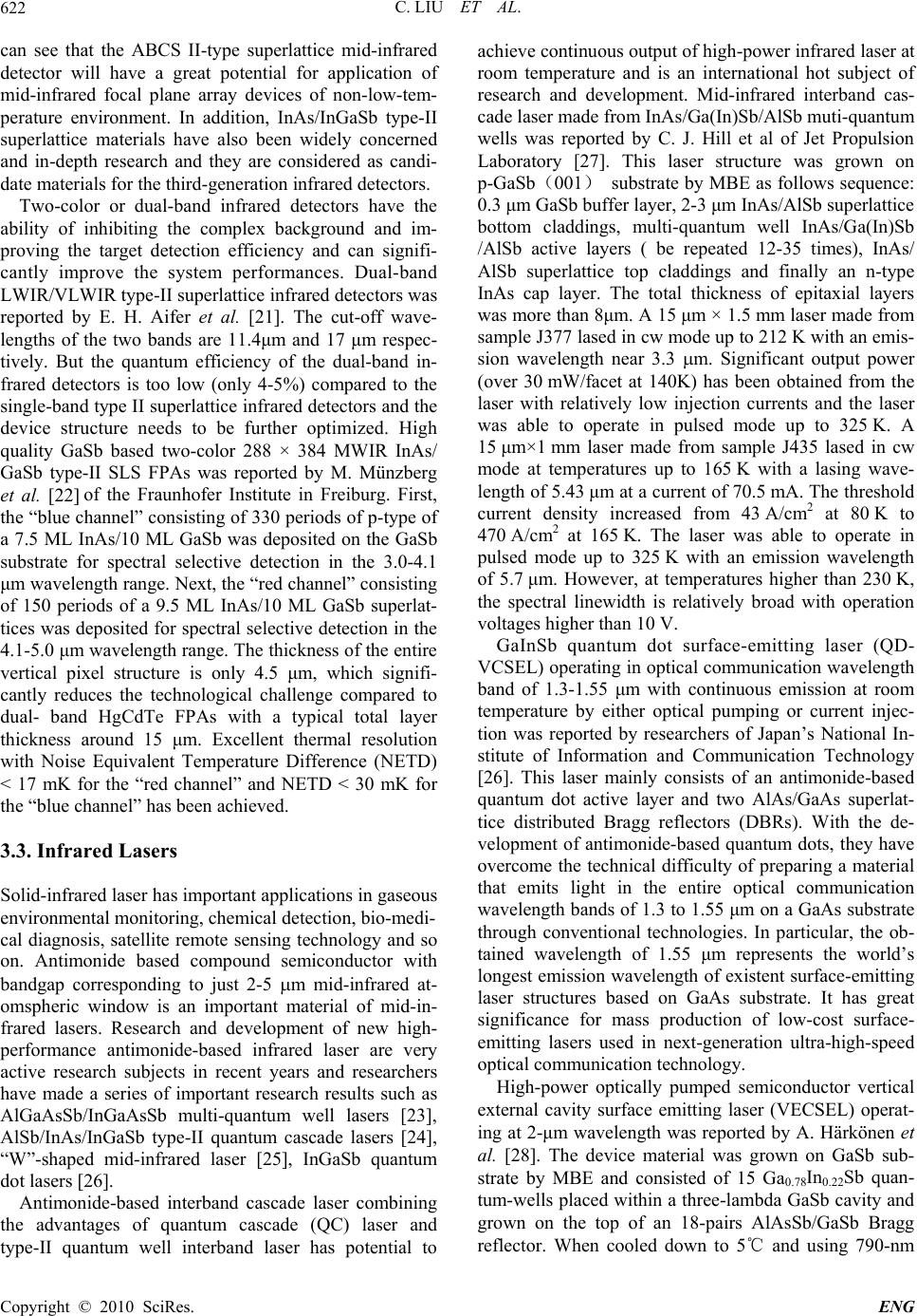 C. LIU ET AL. Copyright © 2010 SciRes. ENG 622 can see that the ABCS II-type superlattice mid-infrared detector will have a great potential for application of mid-infrared focal plane array devices of non-low-tem- perature environment. In addition, InAs/InGaSb type-II superlattice materials have also been widely concerned and in-depth research and they are considered as candi- date materials for the third-generation infrared detectors. Two-color or dual-band infrared detectors have the ability of inhibiting the complex background and im- proving the target detection efficiency and can signifi- cantly improve the system performances. Dual-band LWIR/VLWIR type-II superlattice infrared detectors was reported by E. H. Aifer et al. [21]. The cut-off wave- lengths of the two bands are 11.4μm and 17 μm respec- tively. But the quantum efficiency of the dual-band in- frared detectors is too low (only 4-5%) compared to the single-band type II superlattice infrared detectors and the device structure needs to be further optimized. High quality GaSb based two-color 288 × 384 MWIR InAs/ GaSb type-II SLS FPAs was reported by M. Münzberg et al. [22] of the Fraunhofer Institute in Freiburg. First, the “blue channel” consisting of 330 periods of p-type of a 7.5 ML InAs/10 ML GaSb was deposited on the GaSb substrate for spectral selective detection in the 3.0-4.1 μm wavelength range. Next, the “red channel” consisting of 150 periods of a 9.5 ML InAs/10 ML GaSb superlat- tices was deposited for spectral selective detection in the 4.1-5.0 μm wavelength range. The thickness of the entire vertical pixel structure is only 4.5 μm, which signifi- cantly reduces the technological challenge compared to dual- band HgCdTe FPAs with a typical total layer thickness around 15 μm. Excellent thermal resolution with Noise Equivalent Temperature Difference (NETD) < 17 mK for the “red channel” and NETD < 30 mK for the “blue channel” has been achieved. 3.3. Infrared Lasers Solid-infrared laser has important applications in gaseous environmental monitoring, chemical detection, bio-medi- cal diagnosis, satellite remote sensing technology and so on. Antimonide based compound semiconductor with bandgap corresponding to just 2-5 m mid-infrared at- omspheric window is an important material of mid-in- frared lasers. Research and development of new high- performance antimonide-based infrared laser are very active research subjects in recent years and researchers have made a series of important research results such as AlGaAsSb/InGaAsSb multi-quantum well lasers [23], AlSb/InAs/InGaSb type-II quantum cascade lasers [24], “W”-shaped mid-infrared laser [25], InGaSb quantum dot lasers [26]. Antimonide-based interband cascade laser combining the advantages of quantum cascade (QC) laser and type-II quantum well interband laser has potential to achieve continuous output of high-power infrared laser at room temperature and is an international hot subject of research and development. Mid-infrared interband cas- cade laser made from InAs/Ga(In)Sb/AlSb muti-quantum wells was reported by C. J. Hill et al of Jet Propulsion Laboratory [27]. This laser structure was grown on p-GaSb(001) substrate by MBE as follows sequence: 0.3 μm GaSb buffer layer, 2-3 μm InAs/AlSb superlattice bottom claddings, multi-quantum well InAs/Ga(In)Sb /AlSb active layers ( be repeated 12-35 times), InAs/ AlSb superlattice top claddings and finally an n-type InAs cap layer. The total thickness of epitaxial layers was more than 8μm. A 15 μm × 1.5 mm laser made from sample J377 lased in cw mode up to 212 K with an emis- sion wavelength near 3.3 m. Significant output power (over 30 mW/facet at 140K) has been obtained from the laser with relatively low injection currents and the laser was able to operate in pulsed mode up to 325 K. A 15 μm×1 mm laser made from sample J435 lased in cw mode at temperatures up to 165 K with a lasing wave- length of 5.43 μm at a current of 70.5 mA. The threshold current density increased from 43 A/cm2 at 80 K to 470 A/cm2 at 165 K. The laser was able to operate in pulsed mode up to 325 K with an emission wavelength of 5.7 μm. However, at temperatures higher than 230 K, the spectral linewidth is relatively broad with operation voltages higher than 10 V. GaInSb quantum dot surface-emitting laser (QD- VCSEL) operating in optical communication wavelength band of 1.3-1.55 μm with continuous emission at room temperature by either optical pumping or current injec- tion was reported by researchers of Japan’s National In- stitute of Information and Communication Technology [26]. This laser mainly consists of an antimonide-based quantum dot active layer and two AlAs/GaAs superlat- tice distributed Bragg reflectors (DBRs). With the de- velopment of antimonide-based quantum dots, they have overcome the technical difficulty of preparing a material that emits light in the entire optical communication wavelength bands of 1.3 to 1.55 μm on a GaAs substrate through conventional technologies. In particular, the ob- tained wavelength of 1.55 μm represents the world’s longest emission wavelength of existent surface-emitting laser structures based on GaAs substrate. It has great significance for mass production of low-cost surface- emitting lasers used in next-generation ultra-high-speed optical communication technology. High-power optically pumped semiconductor vertical external cavity surface emitting laser (VECSEL) operat- ing at 2-μm wavelength was reported by A. Härkönen et al. [28]. The device material was grown on GaSb sub- strate by MBE and consisted of 15 Ga0.78In0.22Sb quan- tum-wells placed within a three-lambda GaSb cavity and grown on the top of an 18-pairs AlAsSb/GaSb Bragg reflector. When cooled down to 5℃ and using 790-nm 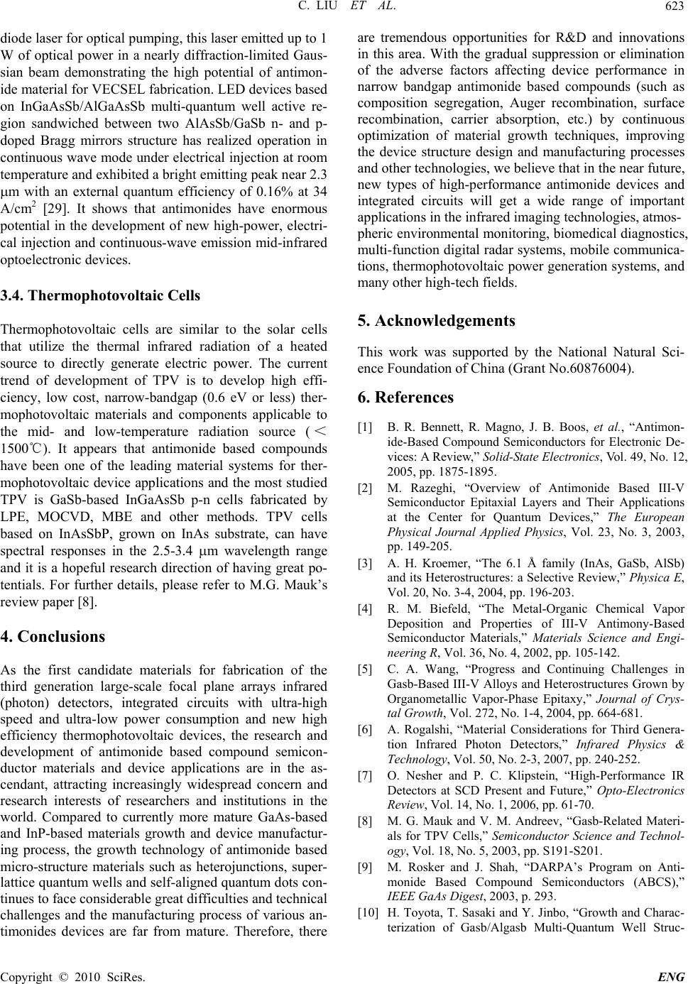 C. LIU ET AL. Copyright © 2010 SciRes. ENG 623 diode laser for optical pumping, this laser emitted up to 1 W of optical power in a nearly diffraction-limited Gaus- sian beam demonstrating the high potential of antimon- ide material for VECSEL fabrication. LED devices based on InGaAsSb/AlGaAsSb multi-quantum well active re- gion sandwiched between two AlAsSb/GaSb n- and p- doped Bragg mirrors structure has realized operation in continuous wave mode under electrical injection at room temperature and exhibited a bright emitting peak near 2.3 m with an external quantum efficiency of 0.16% at 34 A/cm2 [29]. It shows that antimonides have enormous potential in the development of new high-power, electri- cal injection and continuous-wave emission mid-infrared optoelectronic devices. 3.4. Thermophotovoltaic Cells Thermophotovoltaic cells are similar to the solar cells that utilize the thermal infrared radiation of a heated source to directly generate electric power. The current trend of development of TPV is to develop high effi- ciency, low cost, narrow-bandgap (0.6 eV or less) ther- mophotovoltaic materials and components applicable to the mid- and low-temperature radiation source (< 1500). It appears that antimonide based compounds ℃ have been one of the leading material systems for ther- mophotovoltaic device applications and the most studied TPV is GaSb-based InGaAsSb p-n cells fabricated by LPE, MOCVD, MBE and other methods. TPV cells based on InAsSbP, grown on InAs substrate, can have spectral responses in the 2.5-3.4 m wavelength range and it is a hopeful research direction of having great po- tentials. For further details, please refer to M.G. Mauk’s review paper [8]. 4. Conclusions As the first candidate materials for fabrication of the third generation large-scale focal plane arrays infrared (photon) detectors, integrated circuits with ultra-high speed and ultra-low power consumption and new high efficiency thermophotovoltaic devices, the research and development of antimonide based compound semicon- ductor materials and device applications are in the as- cendant, attracting increasingly widespread concern and research interests of researchers and institutions in the world. Compared to currently more mature GaAs-based and InP-based materials growth and device manufactur- ing process, the growth technology of antimonide based micro-structure materials such as heterojunctions, super- lattice quantum wells and self-aligned quantum dots con- tinues to face considerable great difficulties and technical challenges and the manufacturing process of various an- timonides devices are far from mature. Therefore, there are tremendous opportunities for R&D and innovations in this area. With the gradual suppression or elimination of the adverse factors affecting device performance in narrow bandgap antimonide based compounds (such as composition segregation, Auger recombination, surface recombination, carrier absorption, etc.) by continuous optimization of material growth techniques, improving the device structure design and manufacturing processes and other technologies, we believe that in the near future, new types of high-performance antimonide devices and integrated circuits will get a wide range of important applications in the infrared imaging technologies, atmos- pheric environmental monitoring, biomedical diagnostics, multi-function digital radar systems, mobile communica- tions, thermophotovoltaic power generation systems, and many other high-tech fields. 5. Acknowledgements This work was supported by the National Natural Sci- ence Foundation of China (Grant No.60876004). 6. References [1] B. R. Bennett, R. Magno, J. B. Boos, et al., “Antimon- ide-Based Compound Semiconductors for Electronic De- vices: A Review,” Solid-State Electronics, Vol. 49, No. 12, 2005, pp. 1875-1895. [2] M. Razeghi, “Overview of Antimonide Based III-V Semiconductor Epitaxial Layers and Their Applications at the Center for Quantum Devices,” The European Physical Journal Applied Physics, Vol. 23, No. 3, 2003, pp. 149-205. [3] A. H. Kroemer, “The 6.1 Å family (InAs, GaSb, AlSb) and its Heterostructures: a Selective Review,” Physica E, Vol. 20, No. 3-4, 2004, pp. 196-203. [4] R. M. Biefeld, “The Metal-Organic Chemical Vapor Deposition and Properties of III-V Antimony-Based Semiconductor Materials,” Materials Science and Engi- neering R, Vol. 36, No. 4, 2002, pp. 105-142. [5] C. A. Wang, “Progress and Continuing Challenges in Gasb-Based III-V Alloys and Heterostructures Grown by Organometallic Vapor-Phase Epitaxy,” Journal of Crys- tal Growth, Vol. 272, No. 1-4, 2004, pp. 664-681. [6] A. Rogalshi, “Material Considerations for Third Genera- tion Infrared Photon Detectors,” Infrared Physics & Technology, Vol. 50, No. 2-3, 2007, pp. 240-252. [7] O. Nesher and P. C. Klipstein, “High-Performance IR Detectors at SCD Present and Future,” Opto-Electronics Review, Vol. 14, No. 1, 2006, pp. 61-70. [8] M. G. Mauk and V. M. Andreev, “Gasb-Related Materi- als for TPV Cells,” Semiconductor Science and Technol- ogy, Vol. 18, No. 5, 2003, pp. S191-S201. [9] M. Rosker and J. Shah, “DARPA’s Program on Anti- monide Based Compound Semiconductors (ABCS),” IEEE GaAs Digest, 2003, p. 293. [10] H. Toyota, T. Sasaki and Y. Jinbo, “Growth and Charac- terization of Gasb/Algasb Multi-Quantum Well Struc-  C. LIU ET AL. Copyright © 2010 SciRes. ENG 624 tures on Si (0 0 1) Substrates,” Journal of Crystal Growth, Vol. 310, No. 1, 2008, pp. 78-82. [11] K. Zaima, R. Hasimoto, M. Ezaki, et al., “Dislocation Reduction of Gasb on Gaas by Metalorganic Chemical Vapor Deposition with Epitaxial Lateral Overgrowth,” Journal of Crystal Growth, Vol. 310, No. 23, 2008, pp. 4843-4845. [12] T. Ashley, L. Buckle,G. W. Smith, et al., ”Dilute An- timonide Nitrides for Very Long Wavelength Infrared Applications,” Proceedings of SPIE, Orlando, 17 May 2006, pp. 62060L. [13] P. H. Jefferson, L. Buckle , B. R. Bennett, et al., “Growth of Dilute Nitride Alloys of Gainsb Lattice-Matched to Gasb,” Journal of Crystal Growth, Vol. 304, No. 2, 2007, pp. 338-341. [14] D. Jackrel, A. Ptak, B. Seth, et al., “Gainnassb Solar Cells Grown by Molecular Beam Epitaxy,” IEEE 4th World Conference on Photovoltaic Energy Conversion. Waikoloa, HI, 2006, pp. 783-786. [15] J. B. Hacker, J. Bergman, G. Nagy, et al., “An Ultra- Low Power Inas/Alsb HEMT W-Band Low-Noise Am- plifier,” IEEE MTT-S International Microwave Sympo- sium, June 2005, pp. 1029-1032. [16] M. K. Kwang, H. S. Jung, E. K. Dong, et al., “The Growth of a Low Defect Inas HEMT Structure on Si by Using an Algasb Buffer Layer Containing Insb Quantum Dots for Dislocation Termination,” Nanotechnology, Vol. 20, No. 22, 2009, p. 225201. [17] A. Rogalski. “New Material Systems for Third Genera- tion Infrared Photo Detectors,” Opto-Electron Review, Vol. 16, No. 4, 2008, pp. 458-482. [18] M. Walther, R. Rehm, J. Schmitz, et al., “Antimony- Based Superlattices for High-Performance Infrared Imag- ers,” Proceedings of SPIE, Orlandoof, 17 March 2008, pp. 69400A-69400A-8. [19] E. Corbin, M. J. Shaw, M. R. Kitchin, et al., “Systematic Study of Type II Ga1−Xinxsb/Inas Superlattices for In- fra-Red Detection in the 10-12 ΜM Wavelength Range,” Semiconductor Science and Technology, Vol. 16, No. 4, 2001, pp. 263-272. [20] C. J. Hill, J. V. Li, J. M. Mumolo, et al., “MBE Grown Type-II MWIR and LWIR Superlattice Photodiodes,” In- frared Physics & Technology, Vol. 50, No. 2-3, 2007, pp. 187-190. [21] E. H. Aifer, J. G. Tischler, J. H. Warner, et al., “Dual Band LWIR/VLWIR Type-II Superlattice Photodiodes,” Proceedings of SPIE, Orlando, 28 March 2005, Vol. 5783, pp. 112-122. [22] M. Münzberg, R. Breiter, W. Cabanski, et al., “Inas/Gasb Type-II Short-Period Superlattices for Advanced Single And Dual-Color Focal Plane Arrays,” Proceedings of SPIE, Orlando, 9 April 2007, Vol. 6542, p. 654206. [23] Y. G. Zhang, Y. L. Zheng, C. Lin, et al., “Continuous Wave Performance and Tunability of MBE Grown 2.1 µM Ingaassb/Algaassb MQW Lasers,” Chinese Physics Letters, Vol. 23, No. 8, 2006, pp. 2262-2265. [24] A. Bauer, F. Langer, M. Dallner, et al., “Emission Wave- length Tuning of Interband Cascade Lasers in the 3-4 µM Spectral Range,” Applied Physics Letters, Vol. 95, No. 25, 2009, p. 251103. [25] W. W. Bewley, J. R. Lindle, C. S. Kim, et al., “Lifetimes and Auger Coefficients in Type-II W Interband Cascade Lasers,” Applied Physics Letters, Vol. 93, No. 4, 2008, p. 041118. [26] N. Yamamoto, “Next-Generation Optical Communica- tions through Nanotechnology,” NICT News, Vol. 353, 2005, pp. 3-4. [27] C. J. Hill and R. Q. Yang, “MBE Growth Optimization of Sb-Based Interband Cascade Lasers,” Journal of Crystal Growth, Vol. 278, No. 1-4, 2005, pp. 167-172. [28] A. Härkönen, M. Guina, O. Okhotnikov,et al., “1-W An- timonide-Based Vertical External Cavity Surface Emit- ting Laser Operating At 2-ΜM,” Optics Express, Vol.14, No. 14, 2006, pp. 6479-6484. [29] A. Ducanchez, L. Cerutti, P. Grech, et al., “Room Tem- perature Continuous Wave Operation of Electrically-Inje- cted Sb-Based RC-LED Emitting Near 2.3 ΜM,” Super- lattices and Microstructures, Vol. 44, No. 1, 2008, pp. 62-69. |