World Journal of Nano Science and Engineering, 2012, 2, 189-195
http://dx.doi.org/10.4236/wjnse.2012.24025 Published Online December 2012 (http://www.SciRP.org/journal/wjnse)
Molecular Dynamics Study on Mechanical Properties in
the Structur e of Self-Assembled Quantum Dot
Tatsuya Yamaguchi1, Ken-ichi Saitoh2*
1System Design Major, Graduate School of Science and Engineering, Kansai University, Suita, Japan
2Department of Mechanical Engineering, Faculty of Engineering Science, Kansai University, Suita, Japan
Email: *saitou@kansai-u.ac.jp
Received November 7, 2012; revised December 1, 2012; accepted December 8, 2012
ABSTRACT
Stress and strain in the structure of self-assembled quantum dots constructed in the Ge/Si(001) system is calculated by
using molecular dynamics simulation. Pyramidal hut cluster composed of Ge crystal with {105} facets surfaces ob-
served in the early growth stage are computationally modeled. We calculate atomic stress and strain in relaxed pyrami-
dal structure. Atomic stress for triplet of atoms is approximately defined as an average value of pairwise (virial) quan-
tity inside triplet, which is the product of vectors between each two atoms. Atomic strain by means of atomic strain
measure (ASM) which is formulated on the Green’s definition of continuum strain. We find the stress (strain) relaxation
in pyramidal structure and stress (strain) concentration in the edge of pyramidal structure. We discuss size dependency
of stress and strain distribution in pyramidal structure. The relationship between hydrostatic stress and atomic volumet-
ric strain is basically linear for all models, but for the surface of pyramidal structure and Ge-Si interface. This means
that there is a reasonable correlation between atomic stress proposed in the present study and atomic strain measure,
ASM.
Keywords: Molecular Dynamics; Self-Assembled Quantum Dot; Germanium; Silicon; Mechanical Property
1. Introduction
The quantum dot (QD) is a nanostructure which is as-
sembled from a few thousand to a few ten of thousand
semiconductor atoms such as silicon (Si) and germanium
(Ge). This micro-scale structure sometimes shows quan-
tum size effect such that carriers or electrons are con-
fined in very small dimensions. Therefore, previous stu-
dies have been developed so as to be applied to high-
performing electronic devices, the quantum dot laser, the
quantum dot solar cell, and so on.
In order to effectively utilize the special performance
of quantum dots (QDs) for actual device behavior, we
need to obtain high-performance QDs by reducing their
size to approximately 15 - 20 nm (comparable with de-
Broglie wave length) or less in x, y and z directions. In
addition, it is also important that, to some extent, QDs do
not include any crystal defect or any impurity atom
which would disturb the uniformity of the laser wave.
For the purpose of satisfying these requirements in the
industrial production, there is a self-organized growth
method. Formation of three-dimensional island, called
Stranski-Krastanov (S-K) growth, is caused by strain
during epitaxial growth due to lattice mismatch between
different crystals in the substrate and the epitaxial layers.
This method has the advantage that it is quite easy to
form dense array of QDs. However, the shortage of uni-
formity in the cluster arrays, often called array defect,
and the dispersion of cluster sizes are still today’s issues
[1]. Moreover, there is the lack of clarity in understand-
ing detailed mechanical properties of QDs. Unique re-
sidual stress and strain distribute in QDs created by S-K
growth. Indeed, atomic configuration and strain field in
QDs is important because they affect QD’s electronic
structure and mechanical property, so the analysis of
X-ray diffraction and electron scattering experiment have
been conducted. As a result, some understanding in re-
gard with the appearance of dot positions and their con-
figurational correlation has been done and creation of an
equilibrium dot shape becomes possible. From now on,
QD will widely prevail as a new nano material and de-
vice architecture, so we should try to evaluate QD’s me-
chanical properties.
There have been studies on measurement of strain in
QDs by using RHEED or XRD [2,3], but these provide
only the average and qualitative estimation. In the case
when experimental measurement is difficult, the com-
puter simulation is often helpful and gives certain in-
sight. There have been the studies on calculating the dis-
*Corresponding author.
C
opyright © 2012 SciRes. WJNSE
T. YAMAGUCHI, K. SAITOH
190
tribution of strain and stress in Ge islands on the Si(001)
surface by means of atomistic simulation [4-6]. Also,
there have been the studies on Ge/Si(001) system as the
model system of hetero-epitaxial growth. Mo et al. suc-
cessfully captured the STM images of Ge surfaces grow-
ing three-dimensionally on Si(001) substrate [7]. In their
work, they found that Ge atoms aggregate on rectangle or
square bases whose edges become along <100> direc-
tions in the Si substrate. Moreover, it has determined that
there is a structure called hut cluster whose facets of Ge
surface might be especially composed of {105} planes,
though the atoms are crystallographically reconstructed.
After further investigations, using STM and quantum
calculation, the pyramidal structural model of QD with
{105} facets has been constructed [1,8].
Therefore, in this article, using molecular dynamics
(MD), we estimate the mechanical properties in the struc-
ture of self-assembled QD in Ge/Si(001) system. We are
focusing on the Ge hut clusters which have observed in
previous researches [1,7]. There are two main species of
hut clusters: pyramids and wedges. We are to computa-
tionally model pyramidal one because it has higher
symmetry and simpler configuration. We will discuss
stress and strain distribution and size dependency of me-
chanical properties in the pyramidal structure. The
knowledge of QD’s mechanical properties that is ob-
tained by MD in this study contributes to electron state
control and strength design of QDs. This serves as guide-
lines for developing QD.
This paper is organized as follows. First, we formulate
atomic strain measure and atomic stress, and show com-
putational setup and conditions for pyramidal QD struc-
ture. Then, the results of MD simulations are shown and
discussed. Finally, we show conclusions for the mecha-
nical properties in pyramidal hut clusters of QDs.
2. Theory
2.1. Empirical Interatomic Potential
In this study, the interatomic potential of Tersoff type
(T3) is used, in which the potential is capable to describe
the covalent bonding in diamond structure such as those
of silicon and germanium crystal. In the formulation of
this potential, bond strength between atoms implicitly
depends on coordination number of each atom and ex-
perimental binding energy obtained as cohesive one is
integrated. Tersoff potential is superior to other many-
body potentials as for accurate reproduction of the elastic
properties [9]. Here, we use potential parameters given
by former reference [10].
2.2. Atomic Strain Measure
In order to estimate the strain in the three-dimensional
structure using computational result obtained by molecular
dynamics (i.e. atomic coordinates), we introduce herewith
an idea of strain measure defined in the atomic scale [11].


 
2
10
20
ijij ijij ij
ij
ur ur
r
 
0

(1)
where α and β are components (α, β = x, y, z). In Equa-
tion (1), all of the components except for uij
α or uij
β (uij is
displacement between atoms i and j) have been calcu-
lated from the reference (undeformed) atomic configura-
tion, ri
α(0). In order to evaluate strain at individual
atomic sites, Equation (1) is simply averaged over the
neighboring atoms with which the atom i interacts, as
follows:
neighbor
1
neighbor
1N
i
j
Nij

(2)
where Nneighbor is the number of neighbors. The value
obtained by Equation (2) shows a local and atomic strain
around the atom i. We call it atomic strain measure
(ASM) of the atom i.
The atomic strain of Si and Ge should be calculated on
the basis of each equilibrium lattice strain. However, the
initial atomic configuration of simulation model is basi-
cally constructed by using lattice constant of Si. So, the
reference atomic distance rij(0) is adjusted properly in
calculating the atomic strain of Ge using Equation (2).
Since actually lattice constant of Ge is 4.2% longer than
that of Si, rij(0) is modified as follow:

Ge-Ge or Ge-Si
0 |01.042
ij ij
rr (3)
2.3. Atomic Stress for Triplet Potential
Stress of an atom is evaluated by derivative of increase
of potential energy with regard to strain. Based on solid
mechanics and elasticity, this potential energy is sup-
posed to be identical to the strain energy which has been
stored by deformation process. The strain is approxi-
mately obtained from directional vector between atoms,
rij, by assuming uniform strain field in the deformation.
In the MD method, atomic stress is strictly formulated
for pairwise interaction (from virial theorem) and is gen-
erally calculated as for pairwise potential. However,
Tersoff potential includes three-body term. So, it is re-
quired that atomic stress for triplet of atoms is approxi-
mately defined as an average value of pairwise (virial)
quantity inside triplet, which is the product of vectors
between each two atoms.
,,
1
2
i
i
ijijjk jk
tottotik iktot
jikkij ijijik ikjk jk
rr rr
EErrE
rr rr rr

 











(4)
Copyright © 2012 SciRes. WJNSE
T. YAMAGUCHI, K. SAITOH 191
j
kik
rrr
ij
(5)
where i is an ideal volume per atom in reference con-
figuration and Etot is total energy of atomic system.
3. Computation Model
In the Si-Ge system, the nanostructure with {105} crys-
talline facets is observed in the early stage of epitaxial
growth of germanium (Ge) atoms. This characteristic
structure is generally called a hut cluster. Hut clusters are
put into two major categories, pyramids and wedges [1].
The pyramid one is computationally modeled in this
study. Figure 1 shows a schematic drawing of geometri-
cal design for the computation model which is originally
and actually confirmed by previous STM observation [7].
The computation model is consists of Si substrate and Ge
atomic layers. The latter is called wetting layer (WL)
being a few ML thick, where 1 ML corresponds to the
thickness of one atomic layer, i.e., one half of lattice
constant. The pyramidal-shaped cluster is formed on the
WL. Both Si and Ge crystals have diamond structures
though the lattice constant of Ge crystal is set up with
that of Si crystal. As a result, initial configuration of Ge
crystal possesses compressive residual stress and/or
strain. Periodic boundary conditions are applied in x- and
z-directions so that the system is modeled on infinite
two-dimensional superlattice. The 2 ML thickness of Si
substrate on the bottom is supposed to be rigid body and
their atomic displacements are to be all frozen. Figure 2
shows the computation model labeled A created as stated
above. Table 1 shows computational parameters of MD
simulation. To investigate size dependency of mechanic-
cal property of QD, we also calculate models B and C
having different sizes from A. In each model, the height
of pyramidal structure is 8 ML, 12 ML and 16 ML, re-
spectively. WL is 4 ML thick. These models are used as
initial atomic configuration for MD simulation.
In order to analyze the strain in the structure, we first
need to obtain a stable crystal structure. The calculation
procedures are as follows:
1) Structural relaxation (100.0 ps) from the initial con-
figuration without control of system temperature (equili-
bration of the structure).
Figure 1. The schema tic drawing of co mputation model ( g eo -
metrical design).
2) The system temperature is dropped down to 300 K
for relatively long steps, by using conventional velocity
scaling method.
3) Equilibrium calculation (20.0 ps) with the control
temperature.
Then, finally, we obtain stable crystal structure. Table
2 shows the detail of these relaxation procedures.
During the procedure 3), we calculate atomic strain
measure (ASM) and atomic stress of individual atoms by
using the formulation, Equation (2) and Equation (4),
described in Section 2 above. ASMs are measured with
regard to reference configuration of atoms and are calcu-
lated from atomic configuration at any time. Since atoms
are moving all the time, the ASM and atomic stress of
y
[0 0 1]
x
[0 1 0]
z
[1 0 0]
Figure 2. The initial atomic configuration of MD simulation
model A.
Table 1. The model parameters used for MD simulation.
Model A B C
Cell size x,y direction [nm] 20.098 25.53030.961
Cell size in y direction [nm] 6.215 25.53030.961
Base length of the pyramid L [nm] 13.580 16.29521.727
Height of the pyramid h [nm] 2.173 3.259 4.345
Height of Ge wetting layer hw [nm] 1.086
Height of Si substrate hs [nm] 2.173
The number of atoms 76134 132076209009
The number of atoms at the pyramid 7684 2162646559
The number of Ge atoms at the
wetting layer 21904 3534451984
The number of Si atoms 46546 75106110466
The angle θ [deg.] 11.3
Table 2. The model parameters used for relaxation calcula-
tion.
Initial temperature [K] 300.0
Time increment [fs] 0.5
Calculation procedure
Model
(1) (2) (3)
A 13,140
B 16,250
The number of time steps
C
50,000
17,400
10,000
Temperature gradient [K/s] –5.0 × 10¹²
Copyright © 2012 SciRes. WJNSE
T. YAMAGUCHI, K. SAITOH
192
individual atom largely fluctuates at every computational
step. Therefore, we impose a time average to ASM and
atomic stress of individual atom so as to exclude unim-
portant fluctuation and make clearer evaluation. Here, we
focus on the ASM (components εxx and εyy) of individual
atoms along the center axis of pyramidal structure.
4. Result and Discussion
Figures 3 and 4 show the distribution of the ASM, view-
ing on the cross-section parallel to xy plane. These are for
the εxx component in the direction of [010] and for the εyy
components in the direction of [001], respectively. As
shown in Figure 3, εxx is almost zero in top of the py-
ramidal structure. It means that strain relaxation occurs in
the pyramidal structure. In addition to that, relatively
large compressive strain is observed in the bottom edge
of the pyramidal structure. Figure 5 shows the schematic
of local compressive strain. This local compressive strain
observed in edge of the pyramidal structure is understood
as a residual strain which is caused by elastic deforma-
tion in x direction ([010]) in the pyramidal structure and
by strong constraint from Si substrate in WL under the
pyramidal structure. As shown in Figure 4, a certain
large tensile strain is also observed in the region marked
by a circle. This is because a stress component perpen-
dicular to the surface (y direction, [001]) is vanished out,
but strain components in other two directions (x and z,
[100]) reside in compressive regime and they cause lat-
eral strain in the y direction.
Figures 6 and 7 show the distribution of ASM for the
εxx and for the εyy on the center line of the pyramid. The
value of abscissa corresponds to 0 - 8 ML for Si substrate
(0 - 2 ML for fixed atoms), 9 - 12 ML for WL, and 13
ML and larger for pyramidal structure of hut cluster, re-
spectively. As shown in Figure 6, the largest compres-
sive ASM of Ge atom in 9 ML (at the interface be-
tweenWL and Si substrate) is found. This is reasonable
because these Ge atoms and Si atoms join coherently and
Ge atoms are subject to constraint from Si substrate at
the bottom. At the top of pyramidal structure, strain
marks peak value due to atomic rearrangement in the
surface. As shown in Figure 7, pyramidal structure and
WL expand in y direction by compressive elastic strain in
x and z directions.
Next, we discuss the size dependency of pyramidal
structure. Figure 8 shows the relation between εxx and the
position normalized by the height of WL and pyramidal
structure. As shown in Figure 8, the distribution of εxx is
identical in every model. Other components of ASM are
obtained in similar trend as εxx. Accordingly, ASM dis-
tribution in pyramidal structure and WL is three-dimen-
sionally identical and is independent of the size of py-
ramidal structure. Furthermore, in spite of atomic struc-
ture, the ASM is continuous smoothly even at the inter-
face between the pyramidal structure and WL.
y
[0 0 1]
x
[0 1 0]
z
[1 0 0]
Strain
relaxation
Higher
compressive
Strain
Figure 3. Distribution of ASM component εxx (cross-section
onto xy plane).
y
[0 0 1]
x
[0 1 0]
z
[1 0 0]
Tensile
strain
Figure 4. Distribution of ASM component εyy (cross-section
onto xy plane).
Figure 5. Residual compressive strain in the edge of pyra-
midal structure.
-1.4
-1.2
-1
-0.8
-0.6
-0.4
-0.2
0
0.2
0 2 4 6 8 10 12 14 16 18 20 22 24 26 28
Atomic strain
ε
xx
[%]
Monolayer [ML]
model A
model B
model C
Figure 6. ASM distribution at every 1 ML: εxx component.
-3.5
-3
-2.5
-2
-1.5
-1
-0.5
0
0.5
1
1.5
0 2 4 6 8 10 12 14 16 18 20 22 24 26 2
ε
yy
Monolayer [ML]
model A
model B
model C
Figure 7. ASM distribution at every 1 ML: εyy component.
Copyright © 2012 SciRes. WJNSE
T. YAMAGUCHI, K. SAITOH
Copyright © 2012 SciRes. WJNSE
193
atomic coordinate normalized by the length L of pyra-
middal structure as abscissa. As shown in Figures 9 and
10, positive σm (i.e. tensile stress) occurs at the surface of
pyramidal structure. On the other hand, negative σm (i.e.
compressive stress) occurs at Ge atoms in Ge-Si interface.
Compressive hydrostatic stress at the Ge-Si interface is
largely owing to the compressive stress in x and z direc-
tions, which is caused by lattice mismatch between Ge
WL and Si substrate. On the other hand, tensile hydro-
static stress at the surface of pyramidal structure is
brought about by surface tension. Accordingly, some
concentration of hydrostatic stress is also observed as a
result of surface atomic reconstruction. It is believed that
contribution of compressive stress in x and z directions
by lattice mismatch to this tensile hydrostatic stress is
smaller because of strain (stress) relaxation in pyramidal
structure. The distribution of σm is smooth even at the
Ge-Si interface, but that at the surface region shows un-
dulation. Atoms in the Ge-Si interface joins coherently.
However, the {105} facet of pyramidal structure has
atomic-scale surface step. The undulation of σm at the
surface of pyramidal structure is caused by the variation
of coordination number of each atoms due to this sur-
face-step structure.
-1.4
-1.2
-1
-0.8
-0.6
-0.4
-0.2
0
0.2
0 0.2 0.4 0.6 0.8
1
Atomic strain
ε
xx
[%]
Height of pyramidal structure [-]
model A
model B
model C
Figure 8. Normalized ASM distribution of each 1 ML in
WL and pyramidal structure: εxx component.
In order to discuss in detail distribution of stress and
strain in pyramidal structure and WL, we also calculate
hydrostatic stress and volumetric strain and focus on size
dependency and correlation of them. Hydrostatic stress
of individual atoms is calculated from atomic stress
components,
3
x
xyyz
miii
i
z


(6)
Figures 9 and 10 show hydrostatic stress σ m
at the
surface of pyramidal structure and the interface between
Ge WL and Si substrate (in the following, it is called
“Ge-Si interface”) beneath the pyramidal structure, re-
spectively.
As shown in Figures 9 and 10, distribution of hydro-
static stress normalized by length L at the surface and
Ge-Si interface is identical, except for the center region.
In these diagrams, hydrostatic stress σm is plotted for
1
1.5
2
2.5
3
0 0.2 0.4 0.6 0.8 1 0
0.2
0.4
0.6
0.8
1
-1.5
-1
-0.5
0
0.5
1
1.5
2
2.5
3
σ
m
[GPa]
x [-]
z [-]
1
1.
5
2
2.
5
3
0 0.2 0.4 0.6 0.8 1 0
0.2
0.4
0.6
0.8
1
-3
-2
-1
0
1
2
3
σ
m
[GPa]
x [-]
z [-]
1
1.
5
2
2.
5
3
0 0.2 0.4 0.6 0.8 1 0
0.2
0.4
0.6
0.8
1
-1.5
-1
-0.5
0
0.5
1
1.5
2
2.5
3
σ
m
[GPa]
x [-]
z [-]
(a) h = 2.173 nm (b) h = 3.259 nm (c) h = 4.345 nm
Figure 9. The distribution of hydrostatic atomic stress σm at surface of pyramidal structure (atomic coordinate normalized
base length L plot along the abscissa).
-3
-2.9
-2.8
-2.7
-2.6
-2.5
-2.4
-2.3
-2.2
0 0.2 0.4 0.6 0.8 1 0
0.2
0.4
0.6
0.8
1
-3.4
-3.2
-3
-2.8
-2.6
-2.4
-2.2
σ
m
[GPa]
x [-]
z [-]
-3
-2.9
-2.8
-2.7
-2.6
-2.5
-2.4
-2.3
-2.2
0 0.2 0.4 0.6 0.8 1 0
0.2
0.4
0.6
0.8
1
-3.6
-3.4
-3.2
-3
-2.8
-2.6
-2.4
-2.2
σ
m
[GPa]
x [-]
z [-]
-3
-2.9
-2.8
-2.7
-2.6
-2.5
-2.4
-2.3
-2.2
0 0.2 0.4 0.6 0.8 1 0
0.2
0.4
0.6
0.8
1
-3.6
-3.4
-3.2
-3
-2.8
-2.6
-2.4
-2.2
σ
m
[GPa]
x [-]
z [-]
(a) h = 2.173 nm (b) h = 3.259 nm (c) h = 4.345 nm
Figure 10. The distribution of hydrostatic atomic stress σm at Ge in between Ge WL and Si substrate under the pyramidal
structure (atomic coordinate normalized base length L plot along the abscissa).
T. YAMAGUCHI, K. SAITOH
194
The reason why the difference at the center occurs is
that the apex of pyramidal structure is the same size but
is not scaled in total size. However, it is believed that
hydrostatic stress at the surface of pyramidal structure
and the Ge-Si interface is constant without dependence
on size of pyramidal structure.
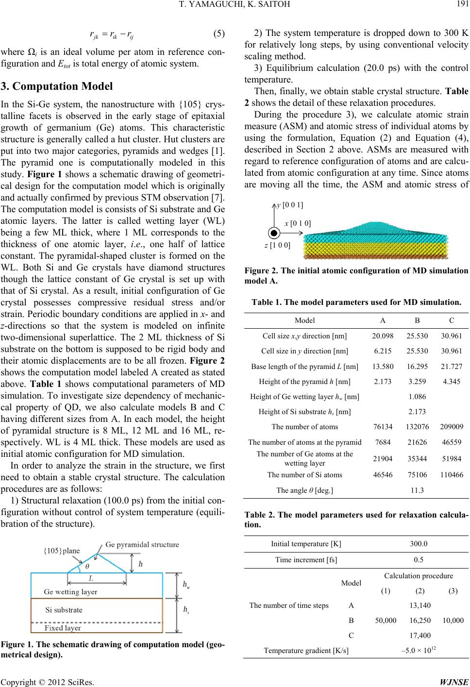
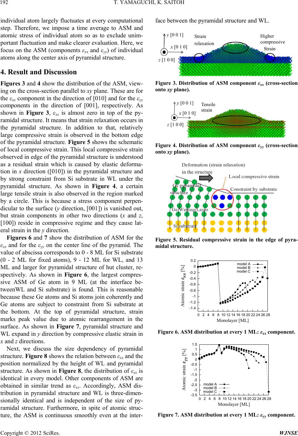
Figures 11 and 12 show the relationship between hy-
drostatic stress σm and atomic volumetric strain εV. Here,
atomic volumetric strain is calculated from components
of ASM, Figure 11 shows plots for atoms on the center
line of the pyramid, just as Figures 6 and 7 above. Sev-
eral plots of positive σm (>0) are found at the surface re-
gion, and their distribution seems at random. Figure 12
is a magnified figure of Figure 11 for its densely plotted
area. The relationship between hydrostatic stress and
atomic volumetric strain is basically linear for all models,
except for the surface of pyramidal structure and Ge-Si
interface. This means that there is a reasonable correla-
tion between atomic stress proposed in the present study
and atomic strain measure, ASM.
5. Conclusions
We perform molecular dynamics simulation for investi-
gating mechanical characteristic in an uncapped pyrami-
dal structure in the Ge/Si(001) system with lattice mis-
match. We estimate the strain by mean of atomic strain
measure (ASM) which is formulated on the Green’s defi-
-6
-4
-2
0
2
4
6
8
-35-30-25-20-15-10-5 0
5
σ
m
[GPa]
ε
V
[%]
model A
model B
model C
Figure 11. The relationship between hydrostatic stress σm
and atomic volumetric strain εV.
-5
-4
-3
-2
-1
0
-2.5-2-1.5-1-0.5 0 0.
5
σ
m
[GPa]
ε
V
[%]
model A
model B
model C
Figure 12. The correlation between hydrostatic stress σm
V
nition of continuum strain and
and atomic volumetric strain ε.
is expressed with atomic
ss in atomic scale can be
qu
strain in x and z directions is
ob
tu
ion between atomic
st
ed by “Strategic Project to
[1] L. V. Arapkintomic Structure of
positions, and atomic stress for triplet interaction. Fol-
lowing results are obtained.
1) Elastic strain and stre
alitatively calculated.
2) Local compressive
served in edge of the pyramidal structure. This local
compressive strain is understood as a residual strain
which is caused by elastic deformation in x and z direc-
tions in the pyramidal structure and by strong constraint
from Si substrate in WL under the pyramidal structure.
3) Hydrostatic stress at the surface of pyramidal struc-
re and the Ge-Si interface is constant without depend-
ence on size of pyramidal structure.
4) There is a reasonable correlat
ress proposed in the present study and atomic strain
measure, ASM, except for the surface of pyramidal struc-
ture and Ge-Si interface.
6. Acknowledgements
This study is partly support
Support the Formation of Research Bases at Private
Universities: Matching Fund Subsidy from MEXT (Min-
istry of Education Culture, Sports, Science and Technol-
ogy) (2012)”.
REFERENCES
a and V. A. Yuryev, “A
Ge Quantum Dots on the Si(001) Surface,” JETP Letters,
Vol. 91, No. 6, 2010, pp. 281-285.
doi:10.1134/S0021364010060056
[2] A. A. Williams, et al., “Strain Relaxation during the Ini-
tial Stages of Growth in Ge/Si(001),” Physical Review B,
Vol. 43, No. 6, 1991, pp. 5001-5011.
doi:10.1103/PhysRevB.43.5001
[3] A. I. Nikiforov, V. A. Cherepanov, O. P. Pchelyakov, A.
V. Dvurechenskii and A. I. Yakimov, “In situ RHEED
Control of Self-Organized Ge Quantum Dots,” Thin Solid
Films, Vol. 380, No. 1-2, 2000, pp. 158-163.
doi:10.1016/S0040-6090(00)01493-0
[4] P. Raiteri, F. Valentinotti and L. Miglio, “Stress, Strain
and Elastic Energy at Nanometric Ge Dots on Si(001),”
Applied Surface Science, Vol. 188, No. 1-2, 2002, pp. 4-8.
doi:10.1016/S0169-4332(01)00702-4
[5] W. Yu and A. Madhukar, “Molecular Dynamics Study of
Coherent Island Energetics, Stresses, and Strains in Highly
Strained Epitaxy,” Physical Review Letters, Vol. 79, No.
5, 1997, pp. 905-908. doi:10.1103/PhysRevLett.79.905
[6] Y. Kikuchi, H. Sugai and K. Shintani, “Strain Profiles in
Pyramidal Quantum Dots by Means of Atomistic Simula-
tion,” Journal of Applied Physics, Vol. 89, No. 2, 2001,
pp. 1191-1196. doi:10.1063/1.1335822
[7] Y.-W. Mo, D.E. Savage, B. S. Swarzentruber and M. G.
Lagally, “Kinetic Pathway in Stranski-Krastanov Growth
of Ge on Si(001),” Physical Review Letters, Vol. 65, No.
Copyright © 2012 SciRes. WJNSE
T. YAMAGUCHI, K. SAITOH 195
8, 1990, pp. 1020-1023.
doi:10.1103/PhysRevLett.65.1020
tability of Ge(105) on [8] Y. Fujikawa, et al., “Origin of the S
Si: A New Structure Model and Surface Strain Relaxa-
tion,” Physical Review Letters, Vol. 88, No. 17, 2002, pp.
176101.1-176101.4. doi:10.1103/PhysRevLett.88.176101
[9] H. Balamane, T. Haliciogau and W. A. Tiller, “Compara-
tive Study of Silicon Empirical Interatomic Potentials,”
Physical Review B, Vol. 46, No. 4, 1992, pp. 2250-2279.
doi:10.1103/PhysRevB.46.2250
[10] J. Tersoff, “Modeling Solid-State Chemistry: Interatomic
Potentials for Multicomponent Systems,” Physical Re-
view B, Vol. 39, No. 8, 1988, pp. 5566-5568.
doi:10.1103/PhysRevB.39.5566
[11] K. Saitoh and W. K. Liu, “Molecular Dynamics Study of
Surface Effect on Martensitic Cubic-to-Tetragonal Trans-
formation in Ni-Al Alloy,” Computational Materials Sci-
ence, Vol. 46, No. 2, 2009, pp. 531-544.
doi:10.1016/j.commatsci.2009.04.025
Copyright © 2012 SciRes. WJNSE