Journal of Modern Physics
Vol.3 No.9(2012), Article ID:22632,10 pages DOI:10.4236/jmp.2012.39140
Preparation and Characterization of ZnO:In Transparent Conductor by Low Cost Dip Coating Technique
1Electronic Materials Department, Advanced Technologies and New Materials Institute, City for Scientific Research and Technological Applications, Alexandria, Egypt
2Physics Department, College of Science, Imam Muhammed Ibn Saud Islamic University, Riyadh, KSA
Email: m.abdelrafea@gmail.com
Received June 18, 2012; revised July 25, 2012; accepted August 2, 2012
Keywords: ZnO:In; TCO; Dip Coating; Optical and Electrical Properties
ABSTRACT
Transparent conducting oxide (TCO) based on indium doped zinc oxide films in the nano scale were successfully prepared using combination between dip coating and thermal decomposition process. Structural investigations confirm the polycrystalline ZnO hexagonal wurtzite phase grown along the c-axis with nano crystallite size about 10 nm. Morphology investigation shows that ZnO films consist of fine grains of average size 40 nm. This indicates that each grain contains several crystallites with different orientations. Cross sectional image presents good adhesion of the films with the substrate and the film thickness has been determined. Compositional analysis detects the indium content in the host ZnO matrix, the In/Zn ratio is close to the calculated concentration ratios of the precursor. The optical transmittance shows that the films are transparent in the UV and VIS-IR spectral region and interference fringes were observed to be thickness dependent. Preparation parameters were investigated and optimized such as dipping rate, number of deposition cycles, precursor concentration, annealing process and In/Zn ratio. Optimization process was investigated for low resistivity, high optical spectral window transmission and easy preparation process. Dipping rate in the range 2 - 38 mm/s is the most suitable range for good film quality while dipping rate range 30 - 38 mm/s produces thicker films in lower deposition cycles. The higher dipping rate produces films with lower transparency (milky films) while the small deposition rate requires large number of deposition cycles in order to increase the thickness. Besides, the higher dipping rate reflects lower resistivity of the deposited films. Precursor molar concentration was observed to have an essential effect on the film thickness, film quality and transparency. Lower precursor concentration requires also large number of deposition cycles for thickening the films. The higher concentration results also milky films (high scattering process by powder film). Precursor concentrations in the range 0.7 - 0.9 mol/liter were found to be the optimal for better quality and for faster deposition process. The resistivity of the films has been reduced from the range 1.5 - 2.5 kW·cm to the range 100 - 400 W·cm as the molar concentration reaches the range 0.07 - 0.09 mol/liter. The resistivity of films increases from 330 to 1686 Ω·cm as the decomposition temperature increases from 200˚C to 350˚C. Annealing at 450˚C process after completing the decomposition at 200˚C results the lowest resistivity with annealing time in the range 1.5 - 2 h. In/Zn percentage in the range 1.5% - 5% produces the lowest electrical resistivity. The absorption edge of the deposited films was observed to be critical affected by the preparation parameters. The band gap change was discussed through the degenerate semiconductors as well as nanostructured semiconducting materials of the energy gap confinement effect. Deposition of TCO based on ZnO:In was optimized depending on all deposition parameters forwide area, the lower cost and good performance TCO films.
1. Introduction
The manufacturing of transparent conducting thin film as transparent conducting electrodes for thin film solar cells has encountered zinc oxide as one of the best options due to high chemical stability against reducing environment [1], a textured surface [2], the simultaneous concurrence of high transparency in the visible region and high conductivity [3]. Some other advantages are the wide material availability, non-toxicity and easy handling that makes ZnO suitable for large area applications [4]. ZnO has direct band gap semiconductor of 3.27 eV and has been recognized for its promising applications in blue/UV optoelectronics, spintronic devices, surface acoustic wave devices and sensor applications [5]. ZnO thin films have been prepared by various deposition techniques, such as RF magnetron sputtering [6-8], spray pyrolysis [9-13], sol-gel process [14-18], electrochemical deposition [19], molecular beam epitaxy (MBE) [20], pulsed laser deposition (PLD) [21-24] and metal organic chemical vapor deposition [25]. However the transport properties of undoped ZnO thin films are not stable, especially at high temperatures due to oxygen. This situation has been improved by introducing impurities into the ZnO host lattice, which dramatically reduces this disadvantage. Doping of ZnO with elements of Group XIII increases in the conductivity of the ZnO thin filmsd. As a matter of fact, the doping of ZnO films by indium [26], aluminum [27], and gallium [28] in ZnO thin films were reported. It is believed that doping process is reached by means of replacing Zn2+ atoms by an impurity with higher valence. It is worth mentioning that the efficiency of the dopant element depends on its electronegativity and difference between its ionic radius in compared with the ionic radius of zinc. Aluminum and indium are well-known dopants for n-type ZnO and have been studied to some extent [29,30]. In comparison with indium tin oxide (ITO), ITO has been mainly used as transparent conducting oxide (TCO) anode because of its high conductivity, large work function and transparency over the visible range [31,32]. Recently, ZnO or doped ZnO has been actively investigated as alternative material due to cost and indium metal availability. In order to examine the suitability of ZnO based TCO, it is essential to deposit it on glass substrate and investigate their optical and electrical properties. We are interested in this study of the deposition parametrs that affect strongly on the transport and optical characteristics of ZnO films deposited by dip coating as low cost, wide area productivity and good film quality in order to compete with the other sophisticated preparation techniques.
2. Experimental Procedures
Thin films of ZnO and ZnO:In with different indium concentrations were prepared by the combination of the dip coating technique and thermal decomposition process. The precursor has been prepared from zinc acetate dehydrate (sigma Aldrich 4N) and dissolved in ethanol (50 mL). The dopant source of indium was indium chloride (sigma Aldrich 5N). Indium chloride was mixed with zinc acetate taking in consideration of atomic percentage of In/Zn atoms in the solution to be in the range 0.0% - 9.0%. The solution was stirred for one hour at 75˚C to yield a clear and homogeneous solution. Pre-cleaned glass micro-slides were coated with the precursor using an automated and homemade dip coater with dipping rate in the range 2 - 40 mm/s. This dip coater is based on falling of the precursor from the dipping tank to another tank by gravity and the flow rate of the precursor was controlled by several diameters of the connecting tube, consequently, the flow rate of the precursor through the connecting tube govern the falling rate of the precursor level in the deposition tank. Falling the precursor level in the deposition tank was calibrated for several rates according to different diameters of the connecting rubber tube between the two tanks as shown in Figure 1 which illustrates the basic diagram of the home made simple dip coater. The top of the deposition tank was covered in order to reduce the evaporation rate of the solvent in which the precursor film drying rate is too small to homogenize the film at the substrate. After dipping process, the films were dried also in air and heated at 200˚C for 10 min in a furnace to decompose the precursor film to ZnO:In. After decomposition process, another deposition cycle was deposited in order to increase the film thickness. Annealing process took place at 450˚C for different annealing times at 1, 2, 3 and 4 h in air. XRD diffractometer of type Shimadzu 7000 XRD, CuKα, Ni filter (λ = 1.5418 Å) was employed in order to identify the crystal structure of the deposited films. The surface morphology was investigated by scanning electron microscopy of type Jeol JSM 6360 OLA. The film adhesion to the substrate and thickness was determined from cross-sectional SEM images. The elemental In:Zn ratio was analyzed by the attached EDX unit to the SEM (Energy dispersive X-ray spectroscopy). Double beam UV-VIS spectrophotometer was used in optical transmittance measurements of the of type LABOMED UVD-2950 spectrophotometer in the wavelength range 190 - 1100 nm using reference substrate. Metallic indium films were deposited using thermal vacuum evaporation technique of type Edwards 306 Auto as electrodes for the deposited ZnO:In using special masks for electrical measurements. Electrical measurements have been performed using Keithely 6517 high performance electrometer.
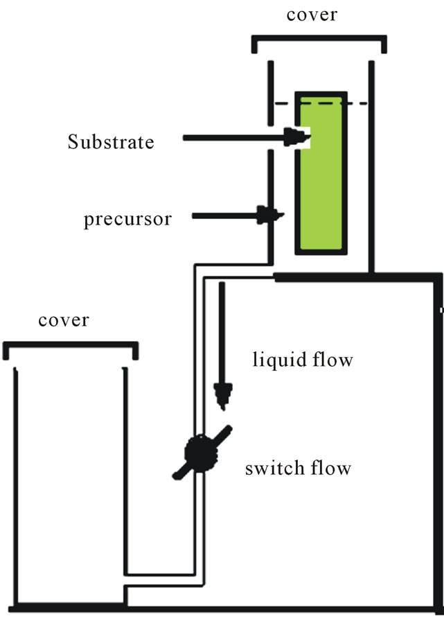
Figure 1. Schematic diagram of the dip coater system.
3. Results and Discussions
3.1. Films Characterization
X-ray diffraction analysis of the deposited film confirms the polycrystalline structure of ZnO films as represented in Figure 2. The diffracted peaks have been identified using standard ZnO cards indicating that all the deposited films are hexagonal wurtzite crystalline phase with (101) preferred orientation. This indicates that the growth process occurs along the c-axis. The diffracted peaks were observed to be broadened. Peak broadening is usually a result of an instrumental broadening, smaller crystallite size and lattice. Other defects have small contribution to the broadening of the diffracted peaks. The instrumental effect was eliminated by measuring standard silicon single crystal free from defects in several crystallographic orientations and the instrumental broadening is set to be βinst. The full width at half maximum for a given peak for the film is βfilm. The peak broadening due to lattice strain and crystallite size is given by:
 (1)
(1)
Applying Williamson-Hall equation for the calculation of crystallite size and lattice strain from the following equation as follows [33,34]:
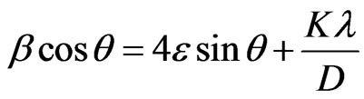 (2)
(2)
where K is the shape factor close to unity, D is the average crystallite size,  is the diffracted angle and
  is the lattice strain. For non strained lattice, Equation (2) is reduced to Scherrer’s equation while in the nano structured materials the strain effect cannot be neglected. By calculating the broadening for diffracted peaks and plotting
  vs
vs , a straight line is obtained of a
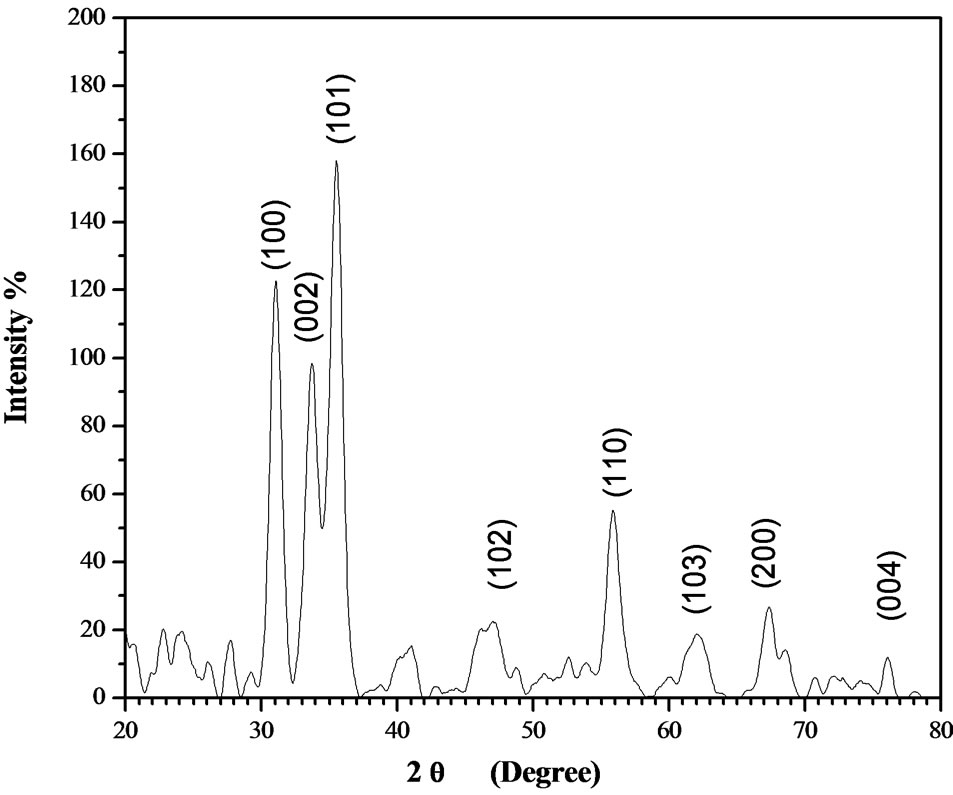
Figure 2. Representative XRD chart of indium doped ZnO thin film with molar ratio 5% on glass substrate.
slop equal to four times of the lattice strain and intercept equal to . The crystallite size of the deposited films was found to be 10 nm. In this case, the deposited films by dip coating technique produces nano structured films and the lattice strain has been observed to be 1.2 × 10⁻⁴ which is considered as very small.
The surface morphology of the In-doped ZnO film has been investigated as shown in Figure 3. Neither cracks nor peels have been observed on the surface of the films. The film consists of fine compact grains of average size 40 nm with high film coverage on the substrate. This means that each grain is not single crystalline because the average crystallites size is 10 nm, i.e. each grain consists of several crystallites with different orientations. Cross sectional image of a broken edge of the substrate shows the film-substrate interface. The thickness of the films is then easily determined from the two film surfaces, besides a good adhesion of the deposition films was observed. The average thickness of the investigated film was found to be 600 nm as represented in sub Figure 3. Energy dispersive x-ray spectroscopy confirms the ZnO atomic percent. The indium atoms percentage is also detected and determined. The indium doped ZnO film by 5% as representative EDX measurement was found to be 5.24% which is compatible with the calculated atomic percent of the precursor. Optical transmittance of films is characterized by open transmittance optical window from the long wavelength and closed from shorter one. The closed edge is found in the UV spectral region which the transparent window cover a wide range of spectrum starting from UV to VIS-IR range as shown in Figure 4. The average optical transmission in the transparent region is in the range 80% - 85% which make those films applicable in optical window applications. Interference fringes were also observed in the optical transmittance due to film two parallel surfaces structure, smooth morphology and higher optical thickness.
3.2. Effect of Deposition Parameters
3.2.1. Effect of Dipping Rate
Dipping rate is generally expressed by the rate of removing the substrate vertically from the precursor, while in our case, the substrate is kept in the deposition tank and the precursor level is decreased as discussed. Dipping rate affects essentially on the amount of the precursor left on the substrate which consequently affects on the thickness of the films as well as the homogeneity. 20 deposition cycles have been performed for each film in order to increase the film thickness. Dipping rate in the range 2 - 40 mm/s was observed to produce good quality film i.e. good transparency and adhesion to the substrate. The optical parameters such as refractive index, extinction
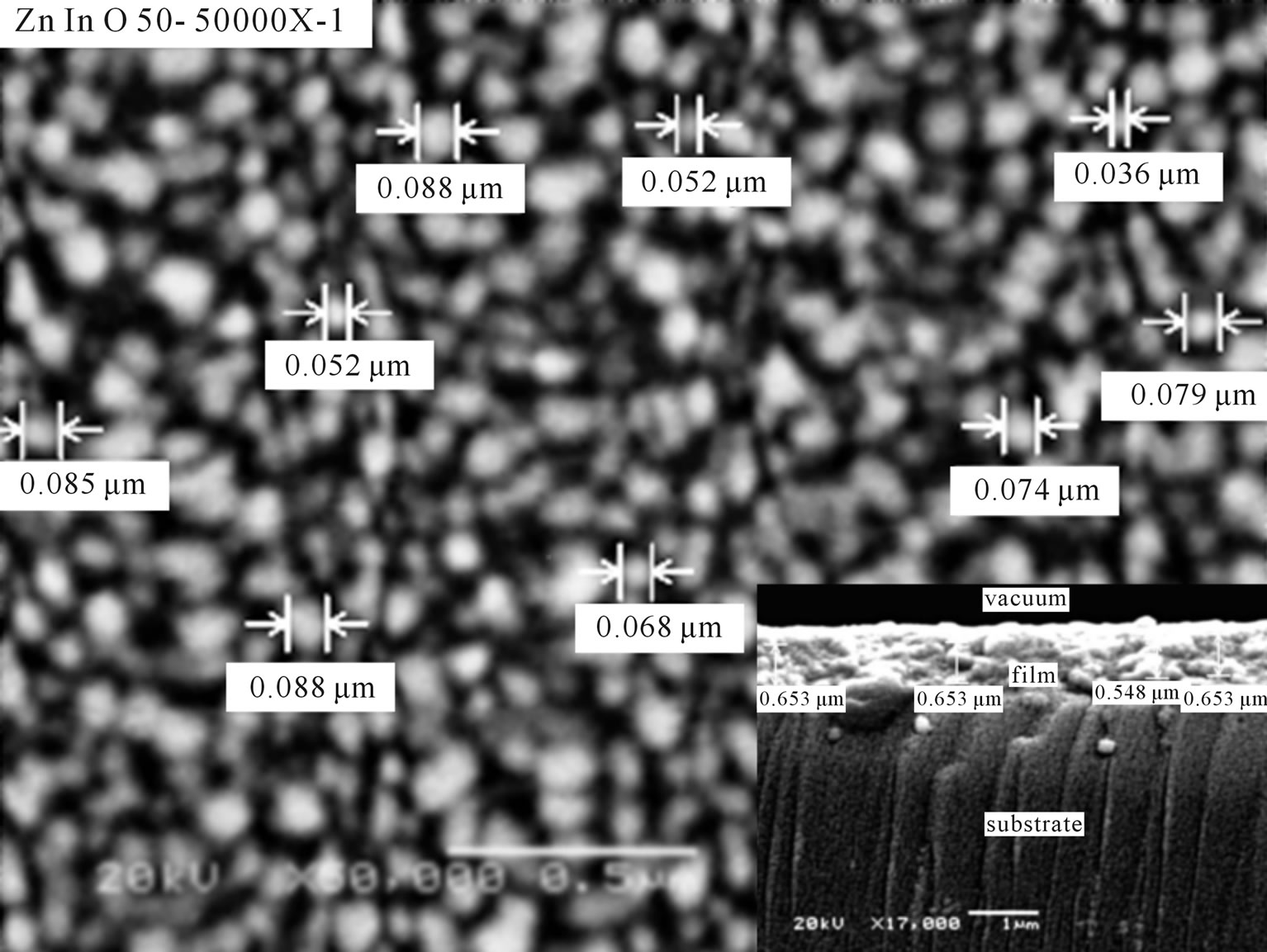
Figure 3. Representative SEM surface image of ZnO:In (5%) and cross sectional image.
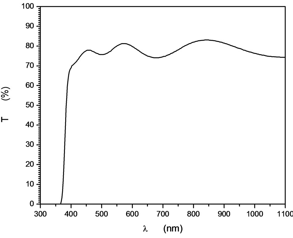
Figure 4. Representative curve of optical transmittance of ZnO:In (5%).
coefficient and band gap were observed to be independent on the dipping rate. Only the interference fringes have been increased as dipping rate increasing. This indicates that the thickness of the films increases. Furthermore, the dipping rate affects on the resistivity as well as films thickness. Figure 5 represents the dependence of the film thickness on the dipping rate. As dipping rate increases the amount of precursor deposited on the substrate increase then evaporation of the solvent occurs before dropping back to the precursor. Lower dipping
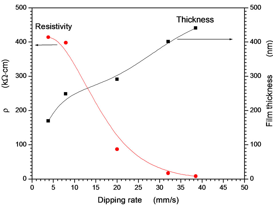
Figure 5. Electrical resistivity and thickness of the film dependence on the dipping rate.
rate produces better film quality and good clearance while the produced thickness is small. The resistivity of the film decreases strongly as increasing the dipping rate due to compactness of the grains by considerable higher deposited amount of the precursor. At very high dipping rate milky and powdered films were obtained, besides at very low dipping rate both the film thickness and compactness of the grins is too low to conduct an electrical current. The studied range of the dipping rate 2 - 40 mm/s is considered as the optimal range for better, clear and electrically conducting films.
3.2.2. Effect of Precursor Concentration
Precursor concentration (mol/liter) governs the film productivity and quality. This study determines the concentration range of the precursor in which the maximum thickness and better quality can be obtained. Molar concentration of zinc acetate in the precursor concentration 0.03 - 0.1 mol/liter was found to be the working concentration for better transparent film. Lower precursor concentration produces films of thickness too small to be produced with several deposition cycles. It required large number of deposition cycles in order to reaches the desired thickness as well as the compactness of the grains is small. At higher precursor concentration than 0.1 mol/ liter, the films were formed as powdered film of particles that agglomerate with bad morphology and consequently the film transparency is too low to be also applicable or measurable. Deposition from precursor concentration in the range 0.03 - 0.1 mol/liter produces high quality films as well as easy production with the desired thickness from few deposition cycles. Figure 6 represents the optical transmittances of ZnO films deposited at different precursor concentration. It was observed that the precursor concentration 0.03 produces films of not complete absorption edge and the first interference fringe is not also completed due to very small thickness. As the precursor concentration increases, the absorption edge reaches full absorption and the interference fringes are completed and their number increases. This indicates that the film thickness increases as the precursor concentration increases. The absorption edge is quite shifted towards longer wavelength as increasing the concentration. This shift was explained as decreasing the band gap. Such band gap shift is a resultant increment of the crystallite size. Smaller crystallites shift the band gap towards the shorter wavelength by the energy gap confinement phenomena which were discussed by the well known Bruss model [35,36] of the nanostructured materials. This model has been discussed in many nanostructured semiconductors. The film transparency was not affected by precursor concentration in this range. Thickness measurement reveals that the thickness increases linearly with the molar concentration of the precursor as shown in Figure 7. The linear fitting of the dependence passes through the origin which indicates the high accuracy of both deposition technique and our results. Electrical resistivity was observed to be higher value in the range 1500 - 2500 Ω·cm at lower precursor concentration range while the resistivity decreases to the range 100 - 400 Ω·cm in the precursor concentration range 0.07 - 0.09 then increases again. The increment of the electrical resistivities in both lower and higher precursor concentration has two different explanations. At lower concentration range of the precursor, the deposited film possesses smaller grains and not compact due to smaller amount of
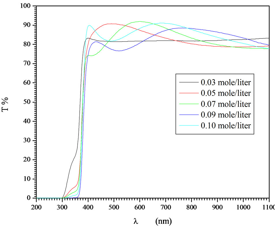
Figure 6. Dependence of electrical resistivity and film thickness on the precursor concentration in the range 0.03 - 0.1 mole/liters.
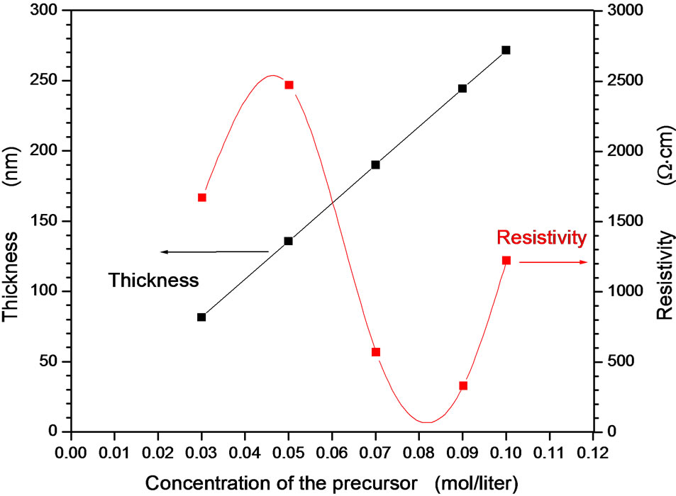
Figure 7. Effect of In doping on ZnO films at different doping percentage 1 - 9 In/Zn%.
the deposited materials. At higher concentration of the precursor, the agglomeration and powdered suspension to the film surface and low adherence of the particles reduce the film conductivity. This indicates that the molar concentration range 0.07 - 0.09 is preferable for considerable high thickness, good film transparency and lower film resistivity.
3.2.3. Effect of Reaction Temperature
Reaction of dried precursor occurs at decomposition of the zinc acetate-ethanol networks and bonds. Dissolving of the zinc acetate with inorganic solvent and drying reduces the decomposition temperature in which ZnO film is formed and other volatile gasses leave the precursor at this temperature. Zinc acetate decomposes at 235˚C to ZnO. This decomposition point was observed to be reduced when the salt was dissolved in ethanol. Studying decomposition process at temperature range 200˚C - 350˚C has been taken into consideration. ZnO films have been deposited from 12 deposition cycles at dipping rate of 20 mm/s and the resultant thickness was 244 nm. The deposition parameters was optimized and selected dependently and used from the previous studies such as precursor concentration and dipping rate. The films possess the same absorption edge and nearly one fringe of interference. It was found that, an increasing of the films resistivity from 330 to 1686 Ω·cm took place when the decomposition temperature increased from 200˚C to 350˚C.
3.2.4. Effect of Indium Doping
Indium doped zinc oxide film was deposited from mixed precursor of indium and zinc salts in the atomic percentage In/Zn 1% - 9%. Indium acetate is insoluble in ethanol so that the chloride salt was chosen. A representative film elemental analysis was confirmed by EDX for actual doping concentration. It is well known that In atoms are easily presented in the ZnO lattice, behave as acceptors, and decreasing the conductivity by increasing the carriers concentration [37]. The optical transmittances of the In-doped ZnO films deposited at 12 dip cycles were observed higher than 80% and IZO films show better transparency than the undoped ZnO. Doping of ZnO by indium in the range 1% - 9% shifts the absorption edge towards the shorter wavelength as shown in Figure 8. The absorption region was magnified by scaling up the absorption region in order to view this shift. Besides, the number of interference fringes and average transmittance in the transparent visible region are also increased as increasing the In/Zn percent. This contribution was explained as the increasing of the optical thickness with increasing the indium content. The shift in the absorption edge was explained to be attributed to carrier concentrations, carrier distributions and defects presented in the film [38]. Based on Manifacier’s model [39], the optical absorption was calculated from the transmittance as shown in Figure 9. ZnO is a direct band gap semiconductor, the relation between the absorption coefficients, (α) and the incident photon energy ( ) is given by [40, 41]:
 (3)
(3)
Plotting of  vs
vs  results a straight line of intercept with at photon energy axis at band gap as shown in Figure 9. It is observed that the band gap is shifted towards UV region as In/Zn percentage increases. The undeped films have a band gap about 3.13 eV which increases gradually as indium content increases as shown in Figure 10. Several reports discussed the energy gap (Eg) change of indium doped ZnO. For example, a report indicates the decrease of the band gap [17,42,43], while other indicates the increase of the band gap [13]. According to our results, i.e. the increment in the band gap by indium doping is logically by two independent effects. The first one is that our films are in the nano scale of size is too small to present the energy gap confinement phenomena as discussed before using Bruss model [35,36]. As the size decreases, the electrons are confined and
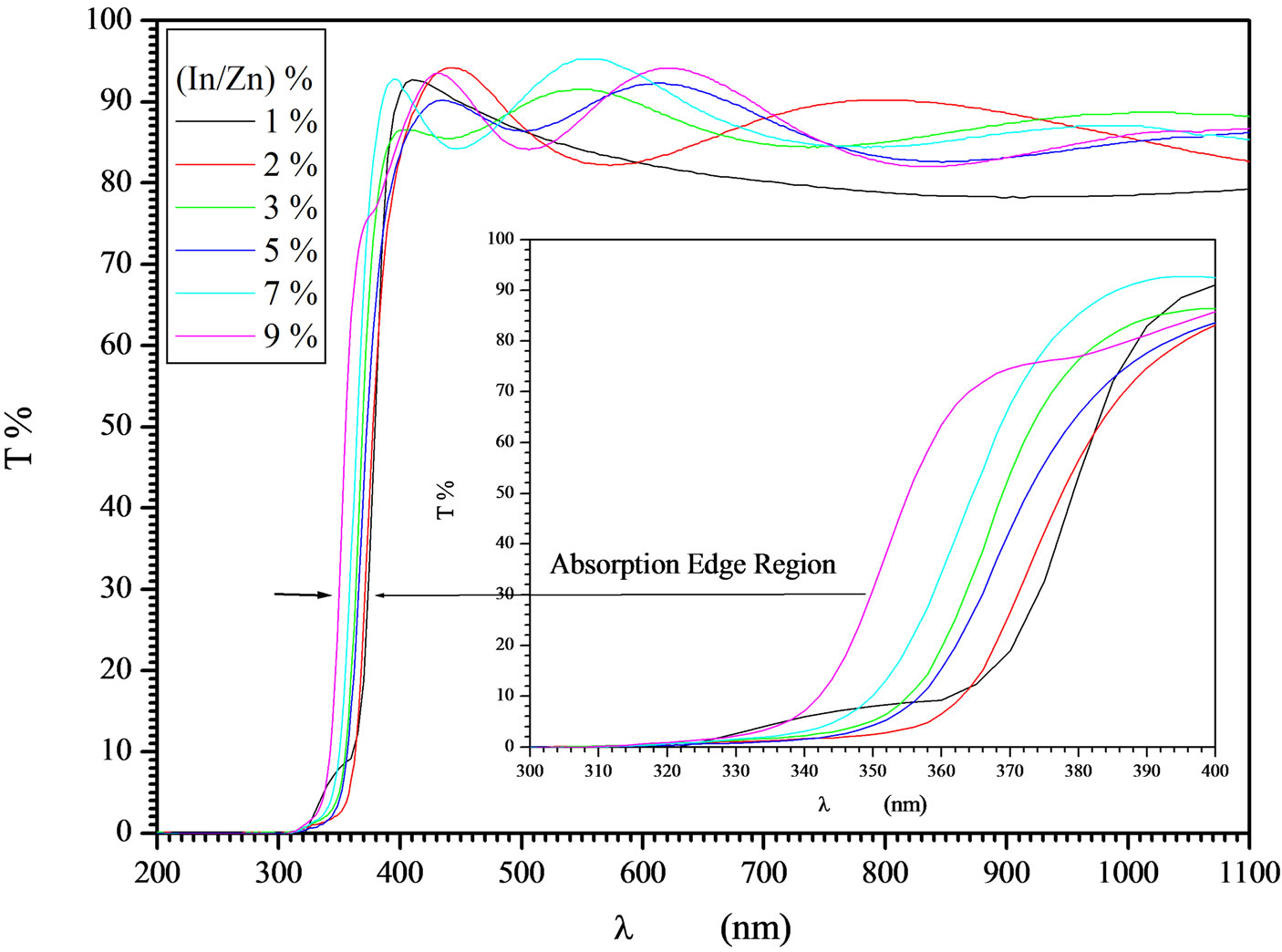
Figure 8. Effect of In doping on ZnO films at different doping percentage 1 - 9 In/Zn %.
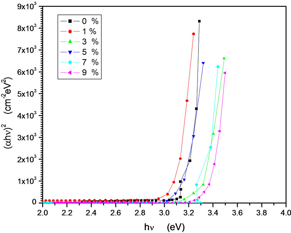
Figure 9. ( )2 vs
)2 vs  for In doped ZnO films at different doping percentage 0 - 9 In/Zn %.

Figure 10. Dependence of film resistivity and band gap on the In/Zn percentage 0% - 9%.
move in a smaller distance comparable or lower than Bohr exciton radius. In this case, the exciton energy is added to the band gap during the absorption process. The second reason of increment of band gap at heavily doped semiconductors. Although, this phenomenon appears at very small density of state effective masses semiconducting materials and or heavily doped or degenerate semiconductors. The Fermi level moves between the valence and conduction bands (forbidden region( at small doping concentration in compared with the total host molecules. It could appear also in heavily doped semiconductors that the Fermi level leaves this forbidden region entering the conduction band in the n-type semiconductor or entering the valence band in the p-type one. In this case, inside the band, the occupation probability above the Fermi level remains very small. At optical absorption process, the transition starts from the occupied state which is not the top of the valence band or the bottom of the conduction band. This means that the transition does not start from the zero momentum. Twice time of the energy difference between the top of the valence band and the Fermi level is then added to the overall the transition energy and appears as an increment in band gap. This phenomenon is well known as Burstein-Moss effect and was discussed in many semiconducting materials of low density of state effective mass and/or heavily doped semiconductors [44,45]. The increment of band gap by both effects in ZnO:In is considered as advantage properties because the optical transmittance window is then enlarged and transmitted more portion of the solar spectrum. The optical refractive index was observed to increase slightly from 1.9 to 1.94 as indium doped ZnO increased to 9%. The electrical resistivity of the films has been studied as a function of the indium doping concentration as shown in Figure 10. Both the undoped and heavily doped films possess higher resistivities while films doped by indium in the doping range 1% - 5% possess the lowest electrical resistivities. The intermediate doping region 1% - 5% was observed to be attractive for many optical and electrical properties. It was suggested to be the optimum conditions for film doping for lower resistive optical window layer. For this reason all of the optimized preparation conditions have been collected dependently in order to prepare a film of doping concentration at 5% with the best other preparation condition in our studies and testing the film at higher annealing temperature at 450˚C for different annealing times 1, 2, 3 and 4 h, the corresponding resistivity of the films were found to be 43, 18.7, 119 and 139.5 W·cm, respectively. Similar kind of results was reported for the film grown by spray pyrolysis technique [10]. This means that the optimal In/Zn percent in the range 1.5% - 5% increases the donor concentration. The donor action of indium compensated the grain boundary scattering leading to decrease in film resistivity. As the doping concentration increased, the grain size decreased due to deformation. Though the carrier concentration is expected to increase by indium doping, the smaller grain size enhances the grain boundary scattering and hence leading to an increase in the resistance at higher indium content.
3.2.5. Effect of Number of Cycles
The number of deposition cycles is mainly governed on the film thickness due to addition of layers to each other. This behavior is linearly if the concentration of the solution does not change during the preparation process. Under long run deposition process, evaporation of the solvent takes place which changes the concentration of the precursor. This study perform the deposition run time according to deposition cycles in which the rate of the increasing the film thickness remains constant. Furthermore, increasing the film thickness by increasing the deposition cycles has a limitation that the film quality and transparency is decreased. Figure 11 shows the optical transmittance of ZnO:In (5%) deposited at 0.09 mol/liter at deposition cycles repeated up to 48 times in order to reach thickness of 627 nm. The optical transmittance was measured every 4 cycles and three representative optical transmittances at deposition cycles 12, 24 and 48 were plotted. It was observed that there is no change in the average transmittance in the transparent region which indicates that the refractive index is kept constant (about 1.9). Furthermore, the number of interference fringes increases due to thickness increase. The calculated optical thickness from the interference fringes indicates that the thickness increases linearly as increasing the deposition cycles until 48 cycles. The best fit pass through origin. The slope of the thickness-number of deposition cycles is 11.5 nm/cycle. This is an important result for design a film of desired thickness that each individual deposition process the film thickness increases by 11.5 nm as represented in Figure 12. A slight shift of the absorption edge towards long wavelength has been observed. The average calculated band gap was found to be 3.2 eV. The slight change in absorption edge with increasing the number of cycles may be attributed to the band shrinkage effect because of increase in carrier concentration [44].
4. Conclusion
Transparent conducting films of indium doped zinc oxide have been successfully deposited in both small and wide areas using novel combination between low cost dip technique and thermal decomposition process. The deposition parameters and conditions for high film transparency in the visible region, wider optical spectrum and lower electrical resistivity have been optimized dependently.
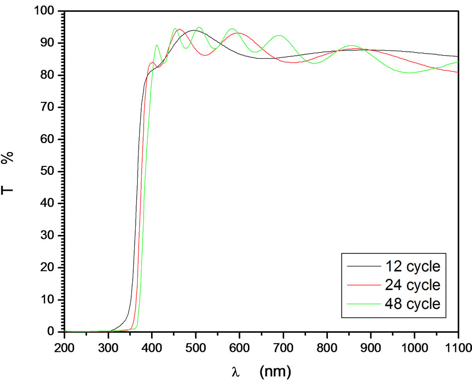
Figure 11. Dependence of deposition cycles on the optical transmittance of ZnO:In.
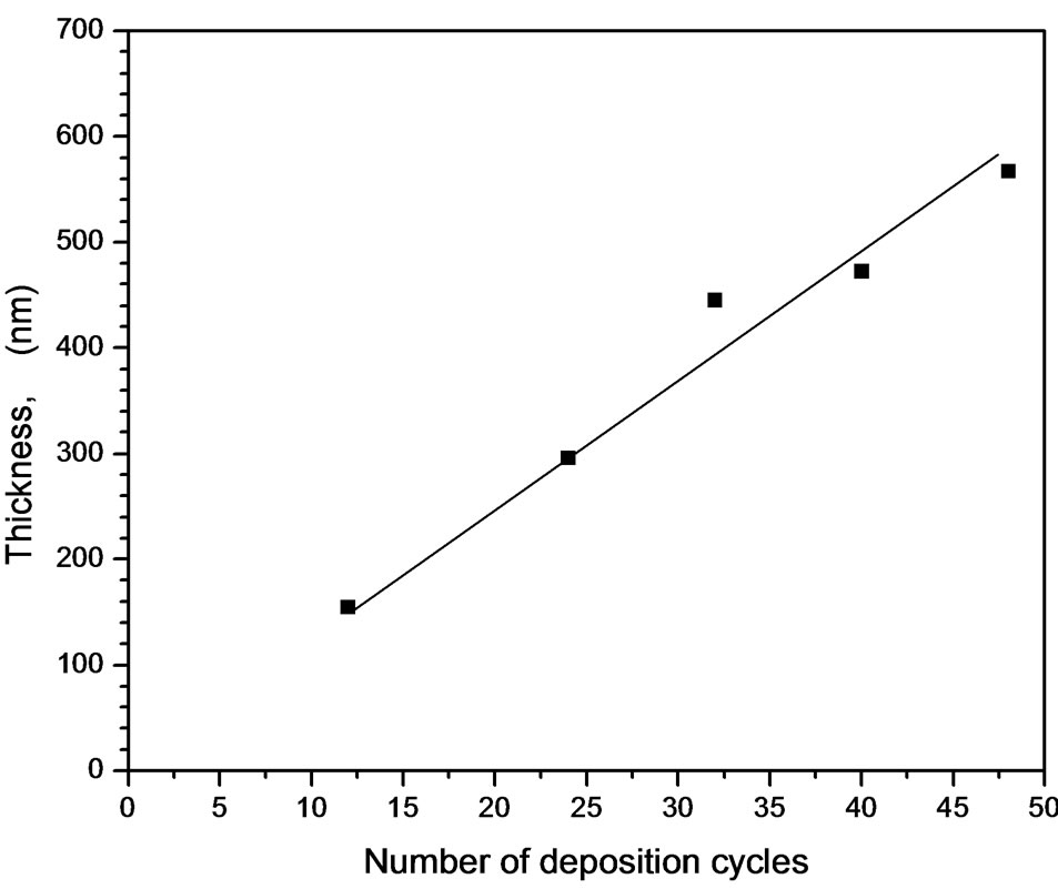
Figure 12. Dependence of deposition cycles on the film thickness.
Films deposited by this technique are characterized by low cost and reproducible for wide area transparent conducting oxide films. The lowering of the resistivity makes those films suitable for many optoelectronic transparent applications such photovoltaic applications and transparent optoelectronics due to their wide spectral window transparency and low resistivity.
5. Acknowledgements
This work was financially supported by the Science and Technology Development Fund (STDF), Egypt, Grant No: ID 1349.
REFERENCES
- A. Ortiz, A. Sanchez, C. Falcony, M. H. Farías, G. A. Hirata and L. Cota-Araiza, “Lack of Chemical Interaction of Hydrogenated Amorphous Silicon with Indium-Doped Zinc Oxide Transparent Conductive Films,” Journal of Non-Crystalline Solids, Vol. 103, No. 1, 1988, pp. 9-13. doi:10.1016/0022-3093(88)90409-7
- M. A. Martinez, J. Herrero and M. T. Gutiérrez, “Deposition of Transparent and Conductive Al-Doped ZnO Thin Films for Photovoltaic Solar Cells,” Solar Energy Materials and Solar Cells, Vol. 45, No. 1, 1997, pp. 75-86.
- S. Oktik, “Low Cost, Non-Vacuum Techniques for the Preparation of Thin/Thick Films for Photovoltaic Applications,” Progress in Crystal Growth and Characterization, Vol. 17, No. 3, 1988, pp. 171-240. doi:10.1016/0146-3535(88)90006-8
- P. S. Patil, “Versatility of Chemical Spray Pyrolysis Technique,” Materials Chemistry and Physics, Vol. 59, No. 3, 1999, pp. 185-198. doi:10.1016/S0254-0584(99)00049-8
- F. K. Shan, B. I. Kim, G. X. Liu, Z. F. Liu, J. Y. Sohn, W. J. Lee, B. C. Shin and Y. S. Yu, “Blueshift of Near Band Edge Emission in Mg Doped ZnO Thin Films and Aging,” Journal of Applied Physics, Vol. 95, No. 9, 2004, pp. 4772-4776. doi:10.1063/1.1690091
- C. J. Xian, J. K. Ahn, N. J. Seong, S. G. Yoon, K. H. Jang and W. H. Park, “Effect of Indium Concentration on the Structural and Electrical Properties of Al-Doped ZnO Thin Films Grown by Pulsed Laser Deposition,” Journal of Physics D: Applied Physics, Vol. 41, No. 21, 2008, Article ID: 215107. doi:10.1088/0022-3727/41/21/215107
- C. Lennon, R. Kodama, Y. Chang, S. Sivanathan and M. Deshpande, “Aland Al:In-Doped ZnO Thin Films Deposited by RF Magnetron Sputtering for Spacecraft Charge Mitigation,” Journal of Electronic Materials, Vol. 37, No. 9, 2008, pp. 1324-1328. doi:10.1007/s11664-008-0436-1
- Y. R. Park, D. Jung, K. C. Kim, S. J. Suh, T. S. Park and Y. S. Kim, “Physical Properties of Transparent Conducting Indium Doped Zinc Oxide Thin Films Deposited by Pulsed DC Magnetron Sputtering,” Journal of Electroceramics, Vol. 23, No. 2-4, 2009, pp. 536-541. doi:10.1007/s10832-008-9530-2
- S. Ilican, Y. Caglar, M. Caglar and B. Demerci, “PolyCrystalline Indium-Doped ZnO Thin Films: Preparation and Characterization,” Journal of Optoelectronics and Advanced Materials, Vol. 10, No. 10, 2008, pp. 2592- 2598.
- P. M. R. Kumar, C. S. Kartha, K. P. Vijayakumar, T. Abe, Y. Kashiwaba, F. Singh and D. K. Avasthi, “On the Properties of Indium Doped ZnO Thin Films,” Semiconductor Science and Technology, Vol. 20, No. 2, 2005, p. 120. doi:10.1088/0268-1242/20/2/003
- M. Caglar, Y. Caglar and S. Ilican, “Electrical and Optical Properties of Undoped and In-Doped ZnO Thin Films,” Physica Status Solidi (C), Vol. 4, No. 3, 2007, pp. 1337-1340. doi:10.1002/pssc.200673744
- K. Krunks, O. Bijakina, V. mikli, T. Varema and E. Mellikov, “Zinc Oxide Thin Films by Spray Pyrolysis Method,” Physica Scripta, Vol. T79, 1999, p. 209. doi:10.1238/Physica.Topical.079a00209
- S. S. Shinde, P. S. Shinde, C. H. Bhosale and K. Y. Rajpure, “Optoelectronic Properties of Sprayed Transparent and Conducting Indium Doped Zinc Oxide Thin Films,” Journal of Physics D: Applied Physics, Vol. 41, No. 10, 2008, Article ID: 105109. doi:10.1088/0022-3727/41/10/105109
- M. Ohyama, H. Kozuka and T. Yoko, “Sol-Gel Preparation of ZnO Films with Extremely Preferred Orientation along (002) Plane from Zinc Acetate Solution,” Thin Solid Films, Vol. 306, No. 1, 1997, pp. 78-85. doi:10.1016/S0040-6090(97)00231-9
- M. Rezaee, R. Abadi, M. Behdani, H. Arabshahi and N. Hosseini, “Indium-Doped Zinc Oxide Thin Films by SolGel Method,” International Review of Physics, Vol. 3, No. 4, 2009, pp. 219-223.
- E. J. L. Arredondo, A. Maldonado, R. Asomoza, D. R. Acosta, M. A. M. Lira and M. de la L. Olvera, “Indium-Doped ZnO Thin Films Deposited by the Sol-Gel Technique,” Thin Solid Films, Vol. 490, No. 2, 2005, pp. 132-136.
- M. Caglar, S. Ilican and Y. Caglar, “Influence of Dopant Concentration on the Optical Properties of ZnO:In Films by Sol-Gel Method,” Thin Solid Films, Vol. 517, No. 17, 2009, pp. 5023-5028. doi:10.1016/j.tsf.2009.03.037
- M. Girtan, M. Socol, B. Pattier, M. Sylla and A. Stanculescu, “On the Structural, Morphological, Optical and Electrical Properties of Sol-Gel Deposited ZnO:In Films,” Thin Solid Films, Vol. 519, No. 2, 2010, pp. 573-577. doi:10.1016/j.tsf.2010.07.006
- G. Machado, D. N. Guerra, D. Leinen, J. R. R. Barrado, R. E. Marotti and E. A. Dalchiele, “Indium Doped Zinc Oxide Thin Films Obtained by Electrodeposition,” Thin Solid Films, Vol. 490, No. 2, 2005, pp. 124-131. doi:10.1016/j.tsf.2005.04.042
- A. Ohtomo, M. Kawasaki, T. Koida, K. Masubuchi, H. Koinuma, Y. Sakurai, Y. Yoshida, T. Yasuda and Y. Segawa, “MgxZn1−xO as a II-VI Widegap Semiconductor Alloy,” Applied Physics Letters, Vol. 72, No. 19, 1998, pp. 2466-2468. doi:10.1063/1.121384
- N. Naghavi, A. Rougier, C. Marcel, C. Gueary, J. B. Leriche and J. M. Tarascon, “Characterization of Indium Zinc Oxide Thin Films Prepared by Pulsed Laser Deposition Using a Zn3In2O6 Target,” Thin Solid Films, Vol. 360, No. 1-2, 2000, pp. 233-240. doi:10.1016/S0040-6090(99)01098-6
- B. Kotlyarchuk, V. Savchuk and M. Oszwaldowski, “Preparation of Undoped and Indium Doped ZnO Thin Films by Pulsed Laser Deposition Method,” Crystal Research and Technology, Vol. 40, No. 12, 2005, pp. 1118- 1123. doi:10.1002/crat.200410502
- K. Ramamoorthy, K. Kumar, R. Chandramohan, K. Sankaranarayana, R. Saravanan, I. V. Kityak and P. Ramasamy, “High Optical Quality IZO (In2Zn2O5) Thin Films by PLD—A Novel Development for III-V Opto-Electronic Devices,” Optics Communications, Vol. 262, No. 1, 2006, pp. 91-96. doi:10.1016/j.optcom.2005.12.042
- R. K. Gupta, K. Ghosh, R. Patel, S. R. Mishra and P. K. Kahol, “Band Gap Engineering of ZnO Thin Films by In2O3 Incorporation,” Journal of Crystal Growth, Vol. 310, No. 12, 2008, pp. 3019-3023. doi:10.1016/j.jcrysgro.2008.03.004
- J. H. Lee and B. O. Park, “Transparent Conducting ZnO:Al, In and Sn Thin Films Deposited by the Sol-Gel Method,” Thin Solid Films, Vol. 426, No. 1-2, 2003, pp. 94-99. doi:10.1016/S0040-6090(03)00014-2
- H. Gomez, A. Maldonado and J. Palacios-Gomez, “Characterization of Indium-Doped Zinc Oxide Films Deposited by Pyrolytic Spray with Different Indium Compounds as Dopants,” Thin Solid Films, Vol. 293, No. 1-2, 1997, pp. 117-123.
- A. F. Aktaruzzaman, G. L. Sharma and L. K. Malhotra, “Electrical, Optical and Annealing Characteristics of ZnO: Al Films Prepared by Spray Pyrolysis,” Thin Solid Films, Vol. 198, 1991, pp. 67-74. doi:10.1016/0040-6090(91)90325-R
- A. Tiburcio-Silver, A. Sanchez-Juarez and A. Avila-Garcia, “Properties of Gallium-Doped ZnO Deposited onto Glass by Spray Pyrolysis,” Solar Energy Materials and Solar Cells, Vol. 55, No. 1-2, 1988, pp. 3-10.
- K. Matsubara, H. Tampo, H. Shibata, A. Yamada, P. Fons, K. Iwata and S. Niki, “Band-Gap Modified Al-Doped Zn1−xMgxO Transparent Conducting Films Deposited by Pulsed Laser Deposition,” Applied Physics Letters, Vol. 85, No. 8, 2004, pp. 1374-1376. doi:10.1063/1.1784544
- T. Minami, K. Oohashi, S. Takata and N. Ogawa, “Preparations of ZnO:Al Transparent Conducting Films by d.c. Magnetron Sputtering,” Thin Solid Films, Vol. 193-194, Part 2, 1990, pp. 721-729. doi:10.1016/0040-6090(90)90224-2
- H. Kim, A. Pique, J. S. Horwitz, H. Mattoussi, H. Murata, Z. H. Kafa and D. B. Chrisey, “Indium Tin Oxide Thin Films for Organic Light-Emitting Devices,” Applied Physics Letters, Vol. 74, No. 23, 1999, pp. 3444-3446. doi:10.1063/1.124122
- H. Kim, C. M. Gilmore, A. Pique, J. S. Horwitz, H. Mattoussi, H. Murata, Z. H. Kafa and D. B. Chrisey, “Electrical, Optical, and Structural Properties of Indium-TinOxide Thin Films for Organic Light-Emitting Devices,” Journal of Applied Physics, Vol. 86, No. 11, 1999, pp. 6451-6461. doi:10.1063/1.371708
- J. Baltazar-Rodrigues, J. C. De Lima, C. E. M. Campos and T. A. Grandi, “Temperature Effects on Mechanically Alloyed Nanometric ZnSe Powder,” Powder Technology, Vol. 189, No. 1, 2009, pp. 70-73. doi:10.1016/j.powtec.2008.06.005
- M. A. Rafea, A. A. M. Farag and N. Roushdy, “Controlling the Crystallite Size and Influence of the Film Thickness on the Optical and Electrical Characteristics of Nanocrystalline Cu2S Films,” Materials Research Bulletin, Vol. 47, No. 2, 2012, pp. 257-266. doi:10.1016/j.materresbull.2011.11.035
- L. E. Brus, “A Simple Model for the Ionization Potential, Electron Affinity, and Aqueous Redox Potentials of Small Semiconductor Crystallites,” Journal of Chemical Physics, Vol. 79, No. 11, 1983, pp. 5566-5571. doi:10.1063/1.445676
- L. E. Brus, “Electron-Electron and Electron-Hole Interactions in Small Semiconductor Crystallites: The Size Dependence of the Lowest Excited Electronic State,” Journal of Chemical Physics, Vol. 80, No. 9, 1984, pp. 4403- 4409. doi:10.1063/1.447218
- G. Sbemeglieri, S. Groppeui, P. Nell, V. Lantto, H. Torvela, P. Romppainen and S. Leppsvuori, “Response to Nitric Oxide of Thin and Thick SnOz Films Containing Trivalent Additives,” Sensors and Actuators, Vol. 1, 1990, pp. 79-82.
- J.-C. Lin, K.-C. Peng, T.-Y. Yeh and S.-L. Lee, “On the Structure and Characterization of Al, Sc-Co-Doped ZnOFilms Varying with 0 - 2.37 wt.% Sc Contents,” Thin Solid Films, Vol. 517, No. 17, 2009, pp. 4715-4719.
- J. C. Manifacier, J. Gasiot and J. P. Fillard, “A Simple Method for the Determination of the Optical Constants n, k and the Thickness of a Weakly Absorbing Thin Film,” Journal of Physics E: Scientific Instruments, Vol. 9, No. 11, 1976, pp. 1002-1004.
- J. I. Pankove, “Optical Processes in Semiconductors,” Prentice-Hall, Englewood Cliffs, 1971.
- V. R. Shinde, T. P. Gujar, C. D. Lokhande, R. S. Mane and S. H. Han, “Mn Doped and Undoped ZnO Films: A Comparative Structural, Optical and Electrical Properties Study,” Materials Chemistry and Physics, Vol. 96, No. 2-3, 2006, pp. 326-330. doi:10.1016/j.matchemphys.2005.07.045
- J. Jie, G. Wang, X. Han, Q. Yu, Y. Liao, G. Li and J. G. Hou, “Indium-Doped Zinc Oxide Nanobelts,” Chemical Physics Letters, Vol. 387, No. 4-6, 2004, pp. 466-470. doi:10.1016/j.cplett.2004.02.045
- L. M. Li, C. C. Li, J. Zhang, Z. F. Du, B. S. Zou, H. C. Yu, Y. G. Wang and T. H. Wang, “Bandgap Narrowing and Ethanol Sensing Properties of In-Doped ZnO Nanowires,” Nanotechnology, Vol. 18, No. 22, 2007, pp. 225504- 225508. doi:10.1088/0957-4484/18/22/225504
- S. Chirakkara, K. K. Nanda and S. B. Krupanidhi, “Pulsed Laser Deposited ZnO:In as Transparent Conducting Oxide,” Thin Solid Films, Vol. 519, No. 11, 2011, pp. 3647- 3652.
- S. Gad, M. A. Rafea and Y. Badr, “Optical and Photoconductive Properties of Pb0.9Sn0.1Se Nano-Structured Thin Films Deposited by Thermal Vacuum Evaporation and Pulsed Laser Deposition,” Journal of Alloys and Compounds, Vol. 515, 2012, pp. 101-107.