Paper Menu >>
Journal Menu >>
 Energy and Power En gineering, 2010, 2, 196-202 doi:10.4236/epe.2010.23029 Published Online August 2010 (http://www.SciRP.org/journal/epe) Copyright © 2010 SciRes. EPE Multi-Bias Model for Power Diode Using a Very High Description Language Hassene Mnif, Montassar Najari, Hekmet Samet, Nouri Masmoudi National Sch o ol of En gi neering of Sfax , LETI Laboratory, Sfax, Tunisia E-mail: hassene.mnif@isecs.rnu.tn Received May 3, 2010; revised June 12, 2010; accepted July 16, 2010 Abstract This study focused on the determination and analysis of an accurate analytical model for PIN diode under different bias conditions. This approach employs analytically derived expressions including the variation of the depletion regions in the device to make the used model available over a wide range of testing conditions without remake the parameters extraction procedure. The validity of the proposed extraction procedure has been verified by the very good agreement between simulated and measured current and voltage waveforms reverse recovery at different range of the operation conditions. The model is developed and simulated with the VHDL-AMS language under Ansoft Simplorer® Environment. Keywords: Power PIN Diode, VHDL-AMS, Modeling, High Injection, Parameter Extraction 1. Introduction Design of integrated power systems requires prototype- less approaches. Accurate simulations are necessary for analysis and verification purposes. Simulation relies on component models and associated parameters. Most of the power PIN diode models provided by the literature are not valid for a mutli-bias simulation be- cause of their limitation to accurately describe the de- vice’s physical rules. One of these physical limitations can be due to sup- posing a fixed depletion region width which is the case of several studies [1]. In [2], the power PIN diode model includes three empirical and non physical equations to escape the extraction procedure when using the model for multi-bias conditions. In this study, the developed power PIN diode model supposes that the width of the intrinsic bulk region is a function of reverse applied voltage as it’s reported by Neudeck and Streetman [3]. Our study is structured as follows. In Section 2, a de- tailed presentation of a new moving boundary diffusion model for the power PIN diodes is made. Section 3 treats the test bench circuit and demonstrates a first comparison with experimental data. Section 4 investigates on the influence of the parasitic inductance in simulation result and the improvement of simulated test circuit by the cor- rection of this parasitic inductance value. Finally, Section 6 gives some conclusions and future study. All the operations (implementation, extraction, optimi- zation …) are made under the free mixed signal simula- tor “Simplorer-sv 7.0” by Ansoft®. 2. PIN Diode Model Description As it is reported in [2], the model is formulated for a P+- IN+ type diode based on the Lauritzen power diode model [1]. Lauritzen and Al.’s model is based on a sys- tematic technique for analytical modeling; the lumped- charge modeling technique (LC) developed by Linvill [4]. Figure 1 shows the charge distribution in a conducting pin diode under forward conduction. The charge distribution in the i-region is assigned to four charge storage nodes following the lumped model approach developed by Linvill [4] with: Figure 1. Charge distribution profile in diode forward conduction [1]. 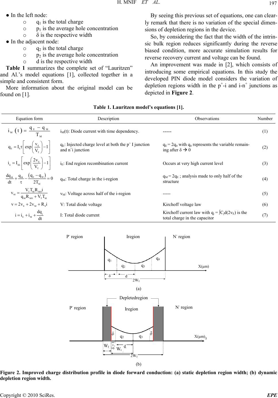 H. MNIF ET AL. Copyright © 2010 SciRes. EPE 197 ● In the left node: o q1 is the total charge o p1 is the average hole concentration o δ is the respective width ● In the adjacent node: o q2 is the total charge o p2 is the average hole concentration o d is the respective width Table 1 summarizes the complete set of “Lauritzen” and Al.’s model equations [1], collected together in a simple and consistent form. More information about the original model can be found on [1]. By seeing this previous set of equations, one can clear- ly remark that there is no variation of the special dimen- sions of depletion regions in the device. So, by considering the fact that the width of the intrin- sic bulk region reduces significantly during the reverse biased condition, more accurate simulation results for reverse recovery current and voltage can be found. An improvement was made in [2], which consists of introducing some empirical equations. In this study the developed PIN diode model considers the variation of depletion regions width in the p+-i and i-n+ junctions as depicted in Figure 2. Table 1. Lauritzen model’s equations [1]. Equation form Description Observations Number EM M M qq it T iM(t): Diode current with time dependency. ----- (1) E ES T v qIexp 1 V qE: Injected charge level at both the p+ I junction and n+i junction qE = 2q0 with q0 represents the variable remain- ing after δ 0 (2) E ESE T 2v iIexp 1 V iE: End region recombination current Occurs at very high current level (3) EM MM M qq dq q0 dt 2T qM: Total charge in the i-region qM = 2qE ; analysis made to only half of the structure (4) TM M0 M MM0 TM VT Ri vqR VT vM: Voltage across half of the i-region ----- (5) EMS v2v 2vRi V: Total diode voltage Kirchoff voltage law (6) j EM dq ii idt I: Total diode current Kirchoff current law with qj = ∫Cjd(2vE) is the total charge in the capacitor (7) Ire gi o n N - regionP - region q 1 q 2 q 3 q 4 d δ 2W I X(μm) (a) Ire gi on N - region P - region W J q 2 q 3 q 01 d δ = 0 2W I X(μm) W t Depletedregion q 04 (b) Figure 2. Improved charge distribution profile in diode forward conduction: (a) static depletion region width; (b) dynamic depletion region width. 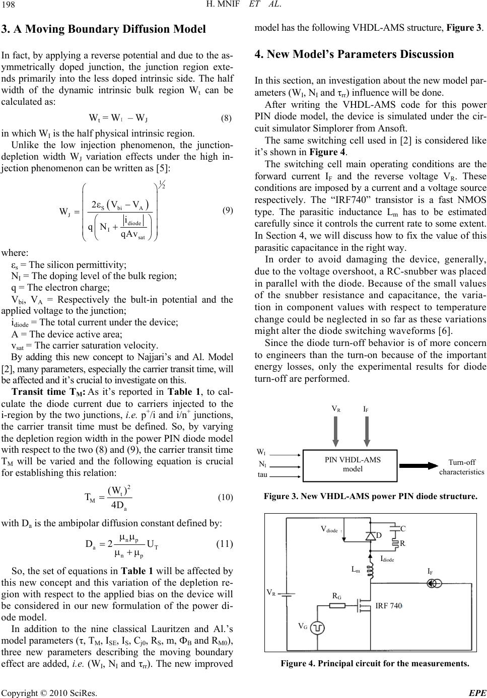 H. MNIF ET AL. Copyright © 2010 SciRes. EPE 198 3. A Moving Boundary Diffusion Model In fact, by applying a reverse potential and due to the as- ymmetrically doped junction, the junction region exte- nds primarily into the less doped intrinsic side. The half width of the dynamic intrinsic bulk region Wt can be calculated as: Wt = WI – WJ (8) in which WI is the half physical intrinsic region. Unlike the low injection phenomenon, the junction- depletion width WJ variation effects under the high in- jection phenomenon can be written as [5]: 12 Sbi A J diode I sat 2VV Wi qN qAv (9) where: εs = The silicon permittivity; NI = The doping level of the bulk region; q = The electron charge; Vbi, VA = Respectively the bult-in potential and the applied voltage to the junction; idiode = The total current under the device; A = The device active area; vsat = The carrier saturation velocity. By adding this new concept to Najjari’s and Al. Model [2], many parameters, especially the carrier transit time, will be affected and it’s crucial to investigate on this. Transit time TM: As it’s reported in Table 1, to cal- culate the diode current due to carriers injected to the i-region by the two junctions, i.e. p+/i and i/n+ junctions, the carrier transit time must be defined. So, by varying the depletion region width in the power PIN diode model with respect to the two (8) and (9), the carrier transit time TM will be varied and the following equation is crucial for establishing this relation: 2 t M a (W ) T4D (10) with Da is the ambipolar diffusion constant defined by: np aT np D2 U (11) So, the set of equations in Table 1 will be affected by this new concept and this variation of the depletion re- gion with respect to the applied bias on the device will be considered in our new formulation of the power di- ode model. In addition to the nine classical Lauritzen and Al.’s model parameters (τ, TM, ISE, IS, Cj0, RS, m, ФB and RM0), three new parameters describing the moving boundary effect are added, i.e. (WI, NI and τrr). The new improved model has the following VHDL-AMS structure, Figure 3. 4. New Model’s Parameters Discussion In this section, an investigation about the new model par- ameters (WI, NI and τrr) influence will be done. After writing the VHDL-AMS code for this power PIN diode model, the device is simulated under the cir- cuit simulator Simplorer from Ansoft. The same switching cell used in [2] is considered like it’s shown in Figure 4. The switching cell main operating conditions are the forward current IF and the reverse voltage VR. These conditions are imposed by a current and a voltage source respectively. The “IRF740” transistor is a fast NMOS type. The parasitic inductance Lm has to be estimated carefully since it controls the current rate to some extent. In Section 4, we will discuss how to fix the value of this parasitic capacitance in the right way. In order to avoid damaging the device, generally, due to the voltage overshoot, a RC-snubber was placed in parallel with the diode. Because of the small values of the snubber resistance and capacitance, the varia- tion in component values with respect to temperature change could be neglected in so far as these variations might alter the diode switching waveforms [6]. Since the diode turn-off behavior is of more concern to engineers than the turn-on because of the important energy losses, only the experimental results for diode turn-off are performed. V R W I I F N I tau Turn-off characteristics PIN VHDL-AMS model Figure 3. New VHDL-AMS power PIN diode structure. C R D V diode V R R G L m V G I diode I F IRF 740 Figure 4. Principal circuit for the measurements.  H. MNIF ET AL. Copyright © 2010 SciRes. EPE 199 4.1. Influence of the Half Physical Intrinsic Region Width WI Under this turn-off state, we perform a simulation of the device with different values of the physical intrinsic re- gion width WI and we capture the curves of the forward current, IF and the reverse voltage, VR. Figure 5 shows that with increasing WI, we give per- mission to the device to accumulate more charge under the on-state. When switched to the off-state, the device gets more time to evacuate these accumulated charges, so we can see a higher maximal reverse voltage and current. 4.2. Influence of the Doping Level NI Figure 6 shows that with increasing the doping profile NI in the device, the device gives more important values of reverse voltage and current. This can be explained by the fact that the depletion region width WJ becomes higher and so, injected charges rise more and more. 4.3. Influence of the Carrier Life Time τ With respect to the following equation of the reverse re- covery time τRR [2]: M RR M T T (12) The plot of Figure 7 is established with supposing a constant transit time set to 22ns. This plotted function is growing-up with increasing the carrier life time τ, i.e., the reverse recovery time τRR is growing-up. In fact, carriers injected to the bulk region recombine less and they have more chances to reach the side con- tacts of the device. So in the turn-off state, the device gives higher values of reverse voltage and current which is mentioned in Figure 8. 4.4. Comparison with Experimental Data The model parameters for the power diode are estimated T i me ( n sec ) 5.00 2.50 0 –2.50 –5.00 –7.50 –10.00 –12.50 –15.00 D i o d e current ( A ) 25.0 50.0 66.7 83.3 100.0 125.0 W 1 = 34.10 -4 cm W 1 = 34, 5.10 -4 cm W 1 = 35.10 -4 cm Figure 5. Influence of the intrinsic region width WI on the diode current turn off characteristic. T i me ( n sec ) 5.00 0 –5.00 –10.00 –15.00 –20.00 –25.00 –30.00 D i o d e current ( A ) 25.0 40.0 60.0 80.0 100.0 120.0 150.0 N 1 = 3.10 14 cm -3 N 1 = 3, 5.10 1 4 cm - 3 N 1 = 4.10 14 cm -3 Figure 6. Influence of the intrinsic region doping NI on the diode current turn off characteristic. τRR ( n sec ) –2.6 × 10 -8 –2.8 × 10 -8 -3 × 10 -8 –3.2 × 10 -8 –3.4 × 10 -8 –3.6 × 10 -8 –3.8 × 10 -8 τRR ( n sec ) 5 × 10 -8 10 × 10 -8 1.5 × 10 -7 2 × 10 -7 Figure 7. Variation of the reverse recovery time τRR in re- spect to the carrier life time τ. T i me ( n sec ) 5.00 2.50 0 –2.50 –5.00 –7.50 –10.00 –12.50 –15.00 D i o d e current (A) 40.0 50.0 62.5 75.0 87.5 100.0 120.0 τ = 100 n sec τ = 200 n sec τ = 400 n sec Figure 8. Influence of the carrier life time τ on the diode current turn off characteristic.  H. MNIF ET AL. Copyright © 2010 SciRes. EPE 200 using the same parameter extraction procedure described in [2] at reverse recovery condition. The Table 2 gives a summary of these model parameters values for the BYT12P600 power diode [7] which are valid for all op- eration conditions. Figure 9 illustrates a comparison of the measured and the simulated voltage and current waveforms for reverse recovery on three different operating conditions: a) VR = 60V and IF = 10A, b) VR = 70V and IF = 2.05A, c) VR = 120V and IF = 10A. The two simulated curves are re- spectively the simulation result of model [2] and the im- proved model developed in this study. These previous Figures 9(a), (b) and (c) show a good agreement between simulation and experimental results except at the end of turn-off where oscillations appear. These oscillations at the end of the reverse recovery voltage waveforms are due to residual phenomena and are very difficult to simulate. However, the effect of these oscillations is not very interesting in design appli- cations [8]. In this figure, the agreement is good enough about the current (IRM and RR) but not so good about the voltage. On the other hand, the estimation of the stray induc- tance in the switching loop of the circuit is critical for modeling the switching process. One cause of error is due to the current and voltage probes. In fact, as stated in [8], probes interact with the device under test, create delays due to propagation in the cable and worst of all degrade the signal due to distortion in the probes and the cables. The overall accuracy of the extraction procedure requires the probe effects to be taken into account in simulation. Simulated forward current curve for the model cited in [2] for IF = 2A and VR = 120A presents an error on the slope compared with the measurement forward current curves. In fact, textbooks [9,10] detail that the diode cur- rent slope is approximated by di/dt = –VR/Lm at the begin- ning of the reverse recovery, inside a switching cell circuit where a unique wiring parasitic inductance is considered. For this reason, an improvement on the parasitic test- bench inductance was made in this work. The next sec- tion will treat this part. 4.5. Parasitic Test Bench Inductance Investigation For estimating the behavior of the device in circuit simu- lation, a complete model of the wiring influence is requi- red which demands the development of a parasitic induc- tive matrix [8]. For more simplicity and short simulation time, in this study, a simple model for this wiring para- sitic is formulated. This simulated test bench inductance improvement is based on the extracted values of Lm (see test bench circuit, Figure 4) from the measured turn-off characteristics according to the following relation: R m V di dt L (13) Figure 10 presents the variation of this test bench parasitic inductance extracted from the measured turn-off characteristics for 3 different test conditions. To capture this inductance influence on the simulated switching cell, a 2nd order polynomial fitting equation is introduced to predict its right value: RR m2 10 FF VV La a a II (14) With a2, a1 et a0 are fitting parameters set to: a2 = 0.0268.109 [HA/V] a1 = 1.3582.109 [HA/V] a0 = 103.19.109 [HA/V] This equation is added to simulated test bench circuit via a VHDL-AMS entity in substitution of the fixed inductance. Figure 9(c) shows the correction of the slope on the simulated current curves compared to measurement. 5. Conclusions A physical improvement is made for a power diode lump- ed-charge model which consists of varying the width of the intrinsic bulk region with respect to the reverse ap- plied voltage and current variations. A second improve- ment is made to the simulated test-bench circuit to esti- mate the right value of the parasitic inductance value. The new model is described in VHDL-AMS language and has been implemented in the SIMPLORER simulator. A good agreement is observed between the new model simulated data and measured data. The results of this improved model are verified with a wide range of oper- ating conditions. This model can be extended by including the selfhea- ting effect which can greatly affect the turn off charac- teristics and the device performance. Table 2. New model’s parameters list. Parameter symbol description Parameter value Unity WI Bulk region width 37.6 µm NI Doping level of the I-region 3.12 × 1014 cm3 carriers lifetime 103.5 n sec TM carriers transit time Equation 10 n sec IS Saturation current 2.78 × 1024 A RM0 Initial resistance 500 Ω ISE Recombination current 45.7386 × 10⁹A Cj0 Junction capacitance 2.2281 nF RS Serial resistance 15.7632 mΩ m Gradient coefficient 430.9960 × 10³-- ФB Bult-in potential 5.9294 mV 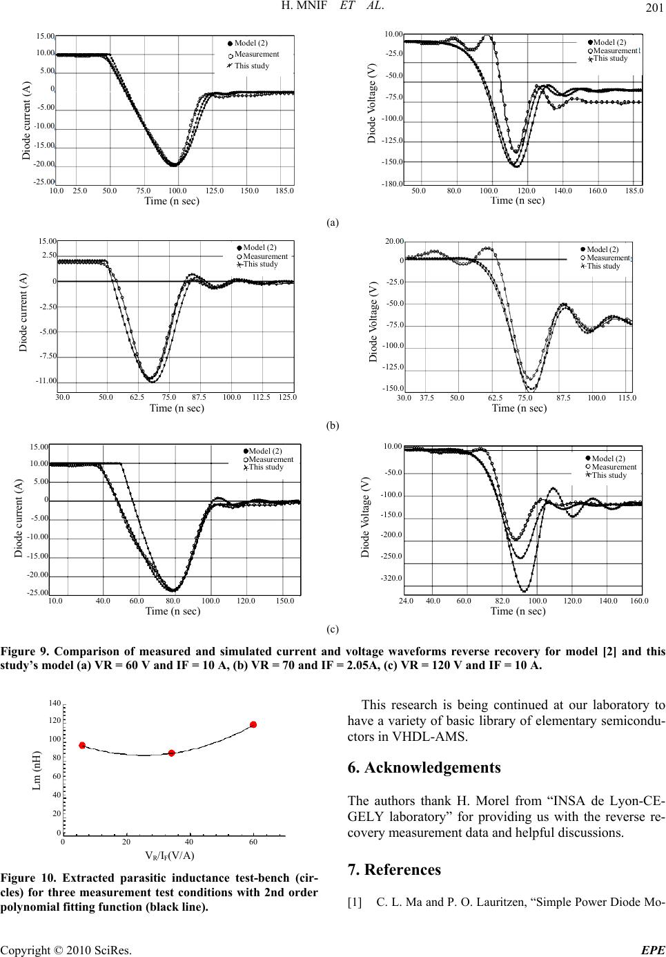 H. MNIF ET AL. Copyright © 2010 SciRes. EPE 201 T i me ( n sec ) 15.00 10.00 5.00 0 -5.00 -10.00 -15.00 -20.00 -25.00 D i o d e current ( A ) 10.0 25.0 50.0 75.0 100.0 125.0 150.0 185.0 Model (2) Measurement This stud y T i me ( n sec ) 10.00 -25.0 -50.0 -75.0 -100.0 -125.0 -150.0 -180.0 D i o d e Vo l tage ( V ) 50.0 80.0 100.0 120.0 140.0 160.0 185.0 Model (2) Measurement This study (a) T i me ( n sec ) 15.00 2.50 0 -2.50 -5.00 -7.50 -11.00 Di o d e current (A) 30.0 50.0 62.5 75.0 87.5 100.0 112.5 125.0 Model (2) Measurement This study T i me ( n sec ) 20.00 0 -25.0 -50.0 -75.0 -100.0 -125.0 -150.0 Di o d e V o l tage ( V ) 30.0 37.5 50.0 62.5 75.0 87.5 100.0 115.0 Model (2) Measurement This study (b) T i me ( n sec ) 15.00 10.00 5.00 0 -5.00 -10.00 -15.00 -20.00 -25.00 D i o d e current ( A ) 10.0 40.0 60.0 80.0 100.0 120.0 150.0 Model (2) Measurement This study T i me ( n sec ) 10.00 -50.0 -100.0 -150.0 -200.0 -250.0 -320.0 D i o d e Vo l tage ( V ) 24.0 40.0 60.0 82.0 100.0 120.0 140.0 160.0 Model (2) Measurement This study (c) Figure 9. Comparison of measured and simulated current and voltage waveforms reverse recovery for model [2] and this study’s model (a) VR = 60 V and IF = 10 A, (b) VR = 70 and IF = 2.05A, (c) VR = 120 V and IF = 10 A. V R / I F ( V / A ) 140 120 100 80 60 40 20 0 Lm ( nH ) 0 20 40 60 Figure 10. Extracted parasitic inductance test-bench (cir- cles) for three measurement test conditions with 2nd order polynomial fitting function (black line). This research is being continued at our laboratory to have a variety of basic library of elementary semicondu- ctors in VHDL-AMS. 6. Acknowledgements The authors thank H. Morel from “INSA de Lyon-CE- GELY laboratory” for providing us with the reverse re- covery measurement data and helpful discussions. 7. References [1] C. L. Ma and P. O. Lauritzen, “Simple Power Diode Mo-  H. MNIF ET AL. Copyright © 2010 SciRes. EPE 202 del with Forward and Reverse Recovery,” IEEE Transac- tions on Power Electronics, Vol. 8, No. 4, 1993, pp. 342- 346. [2] M. Najjari, H. Mnif, H. Samet and N. Masmoudi, “New Modeling of the Power Diode Using the VHDL-AMS Language,” The European Physical Journal Applied Phy- sics, Vol. 4, No. 1, 2008, pp. 1-11. [3] H. Zhang and J. A. Pappas, “A Moving Boundary Diffu- sion Model for PIN Diodes,” IEEE Transactions on Mag- net, Vol. 37, No. 1, 2001, pp. 406-410. [4] P. Antognetti and G. Massobrio, “Semiconductor Device Modeling with SPICE,” MCGraw-Hill Inc, New York, 1988. [5] C. L. Ma and P. O. Lauritzen, “Modeling of Diodes with the Lumped-charge Modeling Technique,” IEEE Trans- actions on Power Electronics, Vol. 12, No. 3, 1997, pp. 398-405. [6] K. X. A. Caiafa, E. Santi, J. L. Hudgins and P. R. Palmer, “Parameter Extraction for a Power Diode Circuit Simu- lator Model Including Temperature Dependent Effects,” 17th Annual IEEE Applied Power Electronics Conference and Exposition, Dallas, March 2002, pp. 452-458. [7] BYT12 600 Datasheet, “Datasheet Archive,” 1998. http:// www.datasheetArchive.com [8] H. Garrab, B. Allard, H. Morel, K. Ammous, S. Ghedira, et al., “On the Extraction of PiN Diode Design Parame- ters for Validation of Integrated Power Converter,” IEEE Transactions on Power Electronics, Monastir, Vol. 20, No. 3, May 2005, pp. 660-670. [9] N. Mohan, T. M. Undeland and W. R. Robbins, “Power Electronics: Converters, Applications and Design,” 2nd Edition, John Wiley & Sons, New York, 1995. [10] R.W. Erickson and D. Maksimovic, “Fundamentals of Power Electronics,” 2nd Edition, Kluwer Academic Pulishers, Berlin, 2001. |