Journal of Electromagnetic Analysis and Applications, 2012, 4, 423-425
http://dx.doi.org/10.4236/jemaa.2012.410058 Published Online October 2012 (http://www.SciRP.org/journal/jemaa) 423
Effect of the Width of the NRD Waveguide on the S
Parameter of a Pass Band Filter
Harizi Hanen1, Lattrach Lassaad1, Gharssallah Ali1, Garbi Abdelhafedh2
1Unit of Research Circuits and Electronics Systems High Frequency, Faculty of Science, University El Manar, Tunis, Tunisia;
2Laboratory of Research Circuits and Electronics Systems High Frequency, Faculty of Science, University El Manar, Tunis, Tunisia.
Email: hanenharizi@gmail.com
Received July 9th, 2012; revised August 18th, 2012; accepted September 3rd, 2012
ABSTRACT
In this paper, we present a design of a non-radiative dielectric waveguide band pass filter based on hybrid architecture
of micro-strip line and non-radiative dielectric waveguide. The simulation with high frequency structure simulator
(HFSS) three dimensional analyses are presented, also the influence of the feeding transitions for circuit design is studied .
The aim of this work was to study the influence of the width of the NRD waveguide to scattering parameters.
Keywords: Non Radiative Dielectric (NRD)
1. Introduction
The technology demand to realize high efficiency circuit,
but productions cost extremely high. Designed for milli-
metre wave, active circuits use planar technology and
passive circuits employ waveguide technologies to inte-
ger those two technologies require highly accurate as-
sembly thus increasing production cost and time. To de-
crease it, the non radiative dielectric waveguide technol-
ogy should be used.
A non-radiative dielectric waveguide is currently in-
teresting filter types due to their high Q at low cost tech-
nology for fabrication and compatibility with other tech-
nology.
Hence their electromagnetic models are still under re-
search and therefore not easy accessible. This work aims
to provide circuit designers with accurate, easy deter-
minable for a pass band filter.
Proposed by Yoneyama and Nishida in 1981 [1], non-
radiative dielectric (NRD) waveguide circuits is nowa-
days a well-known technology for various millimeter-
wave applications [2,3]. Subsequently, Bacha has pro-
posed the model of a hybrid integration of NRD-
waveguide and micro-strip line [4,5]. Indeed, basic fea-
tures and applications of the NRD-waveguide had been
investigated by different research, since it permits to ex-
ploit inherent advantages of planar structures and NRD
waveguide for low cost microwave application. However,
several techniques wer e proposed, Grigoropoulos and Young
present a non-radiative perforated dielectric (NRPD) in
[6], Cassivi and Wu introduce the substrate integrated
non-radiative dielectric (SINRD) [7]. Other scheme of
design called engraved non-radiative dielectric waveguide
(ENRD), proposed to reduce the problem of alignment
and mechanical tolerances in fabrication of NRD com-
ponents, this design was described in [8,9].
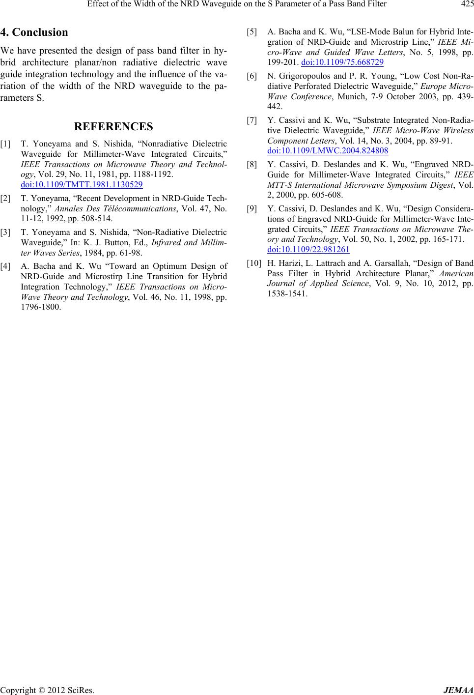
The reference [10] presents the design of pass band
filter in hybrid architecture planar/non radiative dielectric
wave guide integration technology and shows parameters
S. In order to optimize the results of this work, we
thought to var y the width of the N RD gu id e and show th e
influence of this variation.
2. Theoretical Approach
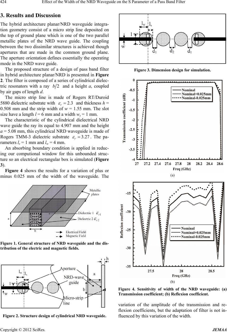
Its basic component, the NRD waveguide consists of a
rectangular-section dielectric rod sandwiched between
conducting plates that are at a distance apart less than
half the free-space wavelength, the thickness is b and the
relative dielectric constant is r
which must be superior
to the relative dielectric constant of the border dielec-
tric.
To express the principle of operation mathematically,
we will consider a straight strip as shown in Figure 1;
the required distance between the two metallic plates of
NRD wave guide is computed using the following rela-
tion:
0
2r
a
where 0
the free-space wavelength r
the relative
dielectric constant.
Copyright © 2012 SciRes. JEMAA