Journal of Modern Physics
Vol.4 No.6(2013), Article ID:33479,12 pages DOI:10.4236/jmp.2013.46120
Theory of Lowand High-Field Transports in Metallic Single-Wall Nanotubes
1Department of Physics, University at Buffalo, Buffalo, USA
2Sincere Learning Centre, Hong Kong, China
3Department of Physics, Faculty of Science, Tokyo University of Science, Tokyo, Japan
Email: fujita@buffalo.edu, hcho@sincerelearning.hk, asuzuki@rs.kagu.tus.ac.jp
Copyright © 2013 Shigeji Fujita et al. This is an open access article distributed under the Creative Commons Attribution License, which permits unrestricted use, distribution, and reproduction in any medium, provided the original work is properly cited.
Received March 21, 2013; revised April 22, 2013; accepted May 18, 2013
Keywords: Metallic SWNT; Orthogonal Unit Cell Model; Supercurrent; Cooper Pair (Pairon); Bloch Electron Dynamics
ABSTRACT
Individual metallic single-wall carbon nanotubes show unusual non-Ohmic transport behaviors at low and high bias fields. For low-resistance contact samples, the differential conductance  increases with increasing bias, reaching a maximum at ~100 mV. As the bias increases further,
  drops dramatically [1]. The higher the bias, the system behaves in a more normal (Ohmic) manner. This low-bias anomaly is temperature-dependent (50 - 150 K). We propose a new interpretation. Supercurrents run in the graphene wall below ~150 K. The normal hole currents run on the outer surface of the wall, which are subject to the scattering by phonons and impurities. The currents along the tube length generate circulating magnetic fields and eventually destroy the supercurrent in the wall at high enough bias, and restore the Ohmic behavior. If the prevalent ballistic electron model is adopted, then the temperature-dependent scattering effects cannot be discussed. For the high bias (0.3 - 5 V), (a) the I-V curves are temperature-independent (4 - 150 K), and (b) the currents (magnitudes) saturate. The behavior (a) arises from the fact that the neutral supercurrent below the critical temperature is not accelerated by the electric field. The behavior (b) is caused by the limitation of the number of quantum-states for the “holes” running outside of the tube.
1. Introduction
In 2000, Yao, Kane and Dekker [1] reported the lowfield and high-field transports in metallic Single-Wall carbon NanoTubes (SWNT). In Figure 1, their I-V curves are reproduced, after Ref. [1], Figure 1. At low fields (voltage ~30 mV), the currents show temperaturedependent dips near the origin, exhibiting non-Ohmic behaviors. The original authors discussed the low-field behavior in terms of one-dimensional (1D) Luttinger liquid (LL) model. Many experiments however indicate that the electrical transports in SWNT have a two-dimensional (2D) character [2]. In fact, the conductivity in individual nanotubes depends on the circumference and the pitch characterizing a space-curve (2D). Hence the nanotube physics requires a 2D theory. Carbon nanotubes are discovered by Iijima [3]. The important questions are how the electrons or other charged particles traverse the nanotubes and whether these particles are scattered by impurities and phonons or not. To answer these questions, we need the electron energy band structures. Wigner and Seitz (WS) [4] developed the WS cell model to study the ground state of a metal. Starting with a given lattice, they obtain a Brillouin zone in the  - space and construct a Fermi surface. This method has been successful for cubic crystals including the facecentered cubic (fcc), diamond and zincblende lattices. If we apply the WS cell model to graphene, we then obtain a gapless semiconductor, which is not experimentally observed [2]. We will overcome this difficulty by taking a different route in Section 2.
SWNTs can be produced by rolling graphene sheets into circular cylinders of about one nanometer (nm) in diameter and microns  in length [5,6]. The electrical conduction in SWNTs depends on the circumference and pitch, and can be classified into two groups: either semiconducting or metallic [2]. In our previous work [7], we have shown that this division in two groups arises as
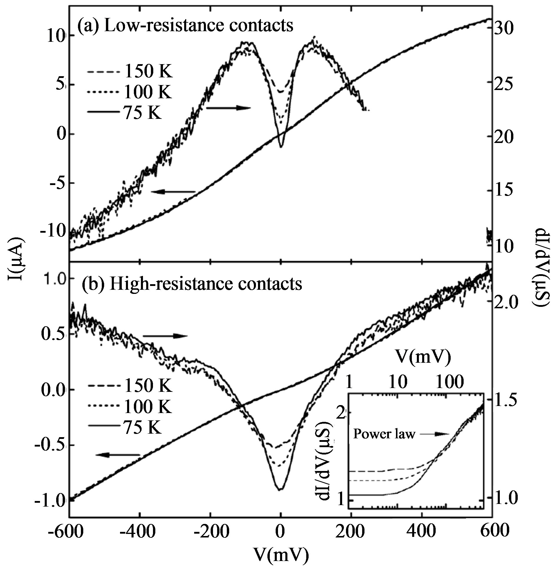
Figure 1. Typical current I and differential conductance dI/dV vs voltage V obtained using (a) low-resistance contacts (LRC) and (b) high-resistance contacts (HRC). The inset to (b) plots dI/dV vs V on a double-log scale for the HRC sample. After Yao et al. [1].
follows. A SWNT is likely to have an integral number of carbon hexagons around the circumference. If each pitch contains an integral number of hexagons, then the system is periodic along the tube axis, and “holes” (not “electrons”) can move along the tube length. Such a system is semiconducting and its electrical conductivity increases with the temperature (semiconductor-like), and is characterized by an activation energy  [8]. The energy
  has a distribution since both pitch and circumference have distributions. The pitch angle is not controlled in the fabrication processes. There are far more numerous cases where the pitch contains an irrational number of hexagons. In these cases, the system shows a metallic behavior experimentally observed [9].
In the present work, we present a unified microscopic theory of both lowand high-field conductivities. We primarily deal with the metallic SWNTs in the present work. Before dealing with high-field transports, we briefly discuss the micro-field (~mV) transports. Tans et al. [10] measured the electrical currents in metallic SWNTs under bias and gate voltages. Their data from Ref. [10], Figure 2, are reproduced in Figure 2. The currents versus the bias voltage are plotted in Figure 2 at three gate voltages: A (88.2 mV), B (104.1 mV), C (120.0 mV). Significant features are:
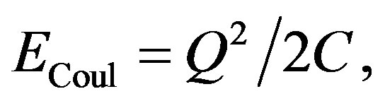
1) A non-Ohmic behavior is observed for all, that is, the currents are not proportional to the bias voltage except for high bias. The gate voltage charges the tube. The Coulomb (charging) energy of the system having charge
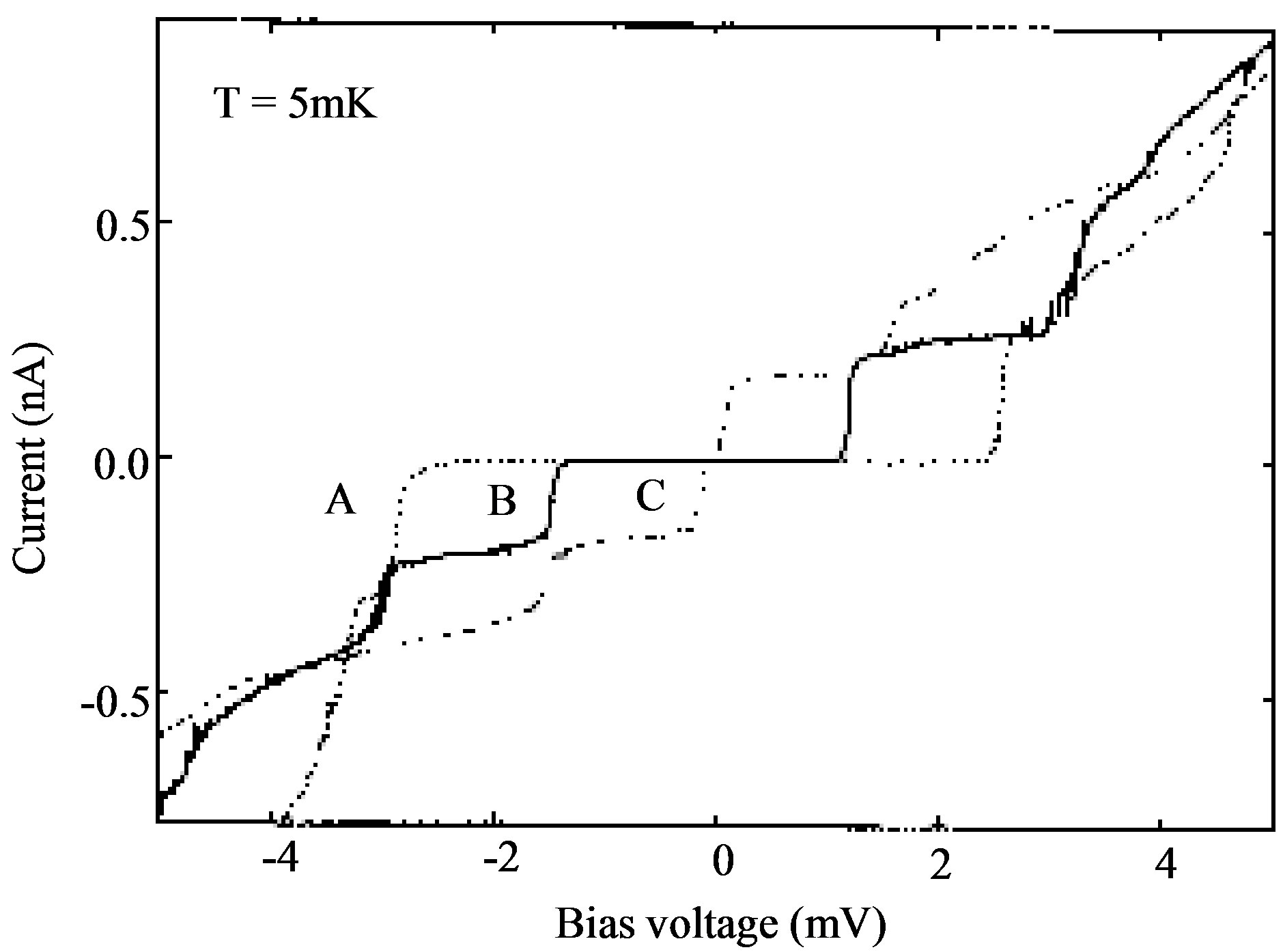
Figure 2. Current-voltage curves of metallic SWNT at gate voltages of 88.2 mV (trace A), 104.1 mV (trace B) and 120.0 mV (trace C). After Tans et al. in Ref. [10], Figure 2.
 is represented by
 (1)
(1)
where  is the total capacitance of the tube.
2) The current near the origin is nearly constant for different gate voltages , (A)-(C). This feature was confirmed by later experiments [9,11]. The current does not change for small varying gate voltage in a metallic SWNT (while the current (magnitude) decreases in a semiconducting SWNT).
3) The current at gate voltage 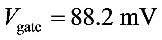 (A) reverts to the normal resistive behavior after passing the critical bias voltages on both (positive and negative) sides. Similar behaviors are observed for
 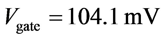 (B) and
 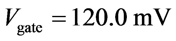 (C).
(C).
4) The flat current is destroyed for higher bias voltages (magnitudes). The critical bias voltage becomes smaller for higher gate voltages.
5) There is a restricted  -range (view window) in which the horizontal stretch can be observed.
Tan et al. [10] interpreted the flat currents near  in Figure 2 in terms of a ballistic electron model [2].
We propose a different interpretation of the data in Figure 2 based on the Cooper pair (pairon) [12] carrier model. Pairons move as bosons, and hence they are produced with no activation energy factor. All features (1) - (5) can be explained simply with the assumption that the nanotube wall is in the superconducting state as explained below.
The supercurrents run without obeying Ohm’s law. This explains the feature (1). The supercurrents can run with no resistance due to the phonon and impurity scattering and with no bias voltage. Bachtold et al. [13] observed by scanned probe microscopy that the currents run with no voltage change along the tube in metallic SWNTs. The system is then in a superconducting ground state, whose energy  is negative relative to the ground-state energy of the Fermi liquid (electron) state. If the total energy
  of the system is less than the condensation energy
 :
:
 (2)
(2)
where  is the kinetic energy of the conduction electrons and the pairons, and
 (3)
(3)
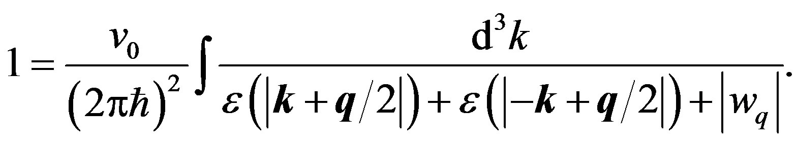
is the Coulomb field energy, then the system is stable. Experiments in Figure 2 were done at 5 mK. Hence, we may drop the kinetic energy  hereafter. The superconducting state is maintained and the currents run unchanged if the bias voltage
  is not too large so that the inequality (2) holds. This explains the horizontal stretch feature (2).
If the bias voltage is high enough so that the inequality symbol in Equation (2) is reversed, then normal currents revert and exhibit the Ohmic behavior, which explains the feature (3).
The feature (4) can be explained as follows. For higher  there is more amount of charge, and hence the charges
 ,
,  ,
,  for the three cases (A, B, C) satisfy the inequalities:
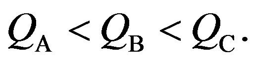 (4)
(4)
The horizontal stretches are longer for smaller bias voltages. At the end of the stretch  the system energy equals the condensation energy
 . Hence, we obtain from Equation (1.2) after dropping the kinetic energy
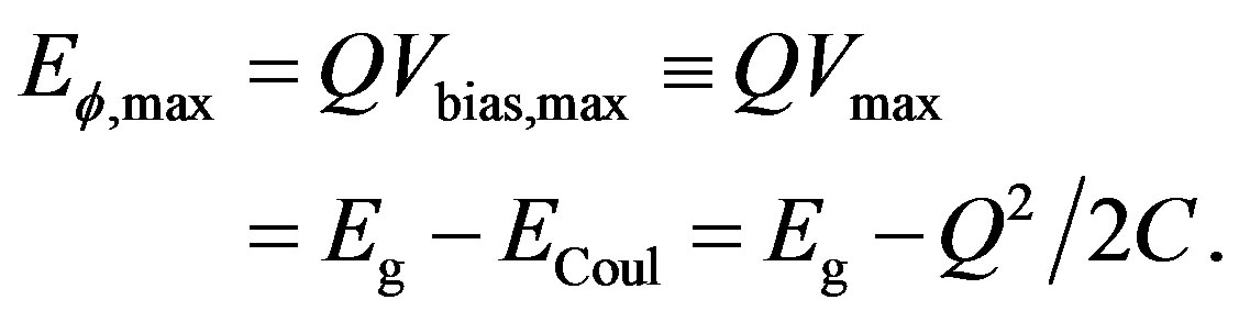 (5)
(5)
Using Equation (1.4), we then obtain
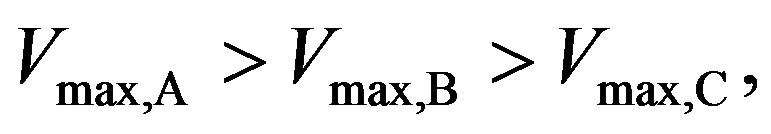 (6)
(6)
which explains the feature (iv).
The horizontal stretch becomes shorter as the gate voltage  is raised; it vanishes when
  is a little over 120.0 mV. The limit is given by
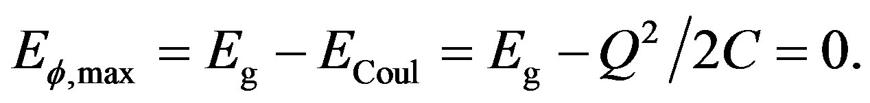 (7)
(7)
If the charging energy  exceeds the condensation energy
 , then there are no more supercurrents, which explains the feature (v). Clearly the important physical property in our pairon model is the condensation energy
 .
.
In the currently prevailing theory [2], it is argued that the electron (fermion) motion becomes ballistic at a certain quantum condition. But all fermions are subject to scattering. It is difficult to justify the reason why the ballistic electron is not scattered by impurities and phonons, which naturally exist in nanotubes. Yao, Kane and Dekker [1] emphasized the importance of phonon scattering effects in their analysis of their data in Figure 1. The Cooper pairs [12] in supercurrents, as is known, can run with no resistance (due to impurities and phonons). The experiments on the currents shown in Figure 1 are visibly temperature-dependent, indicating the importance of the electron-phonon scattering effect. If the ballistic electron model is adopted, then the phonon scattering cannot be discussed within the model’s framework. We must go beyond the ballistic electron model.
Yao et al. [1] extended the I-V measurements up to 5 V as shown in Figure 3, reproduced from Ref. [1], Figure 2. The resistance R versus the bias voltage V shows a relation:
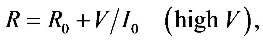 (8)
(8)
where  and
and  are constants. Strikingly, the I-V curves at great bias measured at different temperatures between 4 K and room temperatures overlap with each other. From the shape of the I-V curves, it is clear that the trend of decreasing conductance continues to high bias. Extrapolating the measured I-V curves to higher voltage would lead to a current saturation, that is, a vanishing conductance.
In the present work, we present a quantum statistical theory of the transports, starting with the crystal structure, establishing the electron energy bands, electron-phonon interaction, the BCS-like Hamiltonian and calculating everything steps by steps.
If the SWNT is unrolled, then we have a graphene sheet, which can be superconducting at a finite temperature. We first study the conduction behavior of graphene in Section 2, starting with the honeycomb lattice and
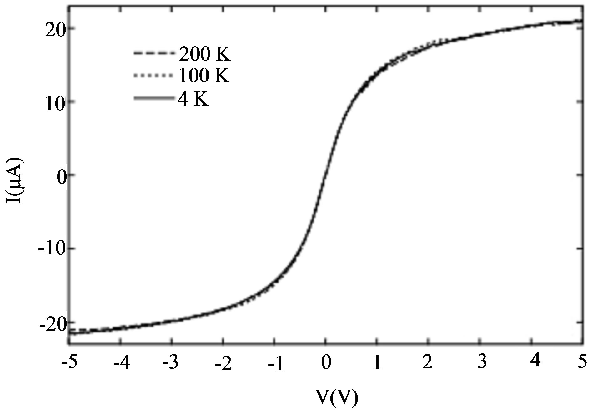
Figure 3. Large-bias I-V curves at different temperatures using low-resistance contacts for a sample with an electrode spacing of 1mm. Note: The curves overlap for different temperatures. The currents (magnitudes) saturate on both sides.
introducing “electrons” and “holes” based on the orthogonal unit cell. Phonons are generated based on the same orthogonal unit cell. In Section 3, we treat phonons and phonon-exchange attraction. In Section 4, we construct a Hamiltonian suitable for the formation of the Cooper pairs. We derive, in Section 5, the linear dispersion relation for the center-of-mass motion of the pairons. The pairons moving with a linear dispersion relation undergoes a Bose-Einstein condensation (BEC) in 2D, which is shown in Section 6. Low-bias anomaly is discussed in Section 7. Current saturation and the temperature behavior are discussed in Section 8. Summary and discussion are given in Section 9.
2. Graphene
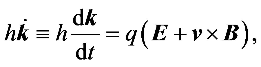
Following Ashcroft and Mermin [14], we adopt the semiclassical model of electron dynamics in solids. In the semiclassical (wave packet) theory, it is necessary to introduce a  -vector:
 (9)
(9)
where ,
,  and
and  are Cartesian orthonormal vectors since the
  -vectors are involved in the semiclassical equation of motion:
 (10)
(10)
where  and
and  are the electric and magnetic fields, respectively, and the vector
 (11)
(11)
is the electron velocity where  is the energy. The 2D crystals such as graphene can also be treated similarly, only the
  -components being dropped. The choice of the Cartesian axes and the unit cell is obvious for the cubic crystals. We must choose an orthogonal unit cell also for the honeycomb lattice, as shown below.
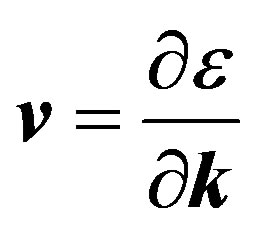
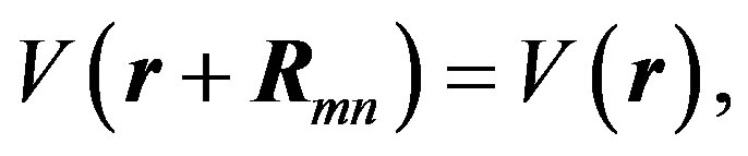
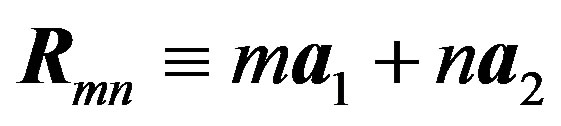
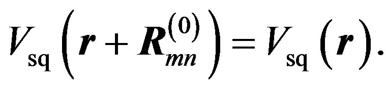
Graphene forms a 2D honeycomb lattice. The WS unit cell is a rhombus shown in Figure 4(a). The potential energy  is lattice-periodic:
Figure 4. (a) WS unit cell, rhombus (dotted lines) for graphene. (b) The orthogonal unit cell, rectangle (dotted lines).
 (12)
(12)
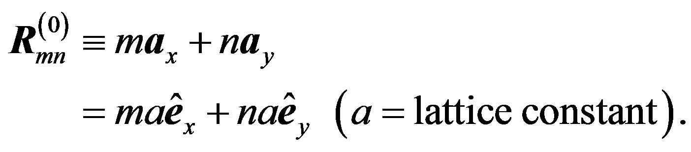
where
 (13)
(13)
are Bravais vectors with the primitive vectors  and integers
 . In the field theoretical formulation, the field point
  is given by
 (14)
(14)
where  is the point defined within the standard unit cell. Equation (12) describes the 2D lattice periodicity but does not establish the
  -space, which is explained below.
To see this clearly, we first consider an electron in a simple square (sq) lattice. The Schrödinger wave equation is
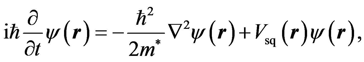 (15)
(15)
where  is the effective electron mass. The Bravais vector for the sq lattice,
  , is
, is
 (16)
(16)
The system is lattice periodic:
 (17)
(17)
If we choose a set of Cartesian coordinates  along the sq lattice, then the Laplacian term in Equation (15) is given by
 (18)
(18)
If we choose a periodic square boundary with the side length ,
,  integer, then there are 2D Fourier transforms and (2D)
  -vectors.
We now go back to the original graphene system. If we choose the  -axis along either
  or
or , then the potential energy field
  is periodic in the x-direction, but it is aperiodic in the
  -direction. For an infinite lattice the periodic boundary is the only acceptable boundary condition for the Fourier transformation. Then, there is no 2D
  -space spanned by 2D
  -vectors. If we omit the kinetic energy term, then we can still use Equation (12) and obtain the ground state energy (except the zero point energy).
We now choose the orthogonal unit cell shown in Figure 4(b). The unit has side lengths
 (19)
(19)
where  is the nearest neighbor distance between two C’s. The unit cell contains 4 C’s. The system is lattice-periodic in the
  - and
- and  -directions, and hence there are 2D
  -space.
The “electron” (“hole”) is defined as a quasi-electron that has an energy higher (lower) than the Fermi energy  and “electrons” (“holes”) are excited on the positive (negative) side of the Fermi surface with the convention that the positive normal vector at the surface points in the energy-increasing direction.
The “electron” (wave packet) may move up or down along the  -axis to the neighboring hexagon sites passing over one C+. The positively charged C+ acts as a welcoming (favorable) potential valley for the negatively charged “electron”, while the same C+ acts as a hindering potential hill for the positively charged “hole”. The “hole”, however, can move horizontally along the x-axis without meeting the hindering potential hills. Thus the easy channel directions for the “electrons” (“holes”) are along the y-(x-)axes.
Let us consider the system (graphene) at 0 K. If we put an electron in the crystal, then the electron should occupy the center O of the Brillouin zone, where the lowest energy lies. Additional electrons occupy points neighboring the center O in consideration of Pauli’s exclusion principle. The electron distribution is lattice-periodic over the entire crystal in accordance with the Bloch theorem [14].
Carbon (C) is a quadrivalent metal. The first few lowlying energy bands are completely filled. The uppermost partially filled bands are important for the transport properties discussion. We consider such a band. The Fermi surface, which defines the boundary between the filled and unfilled k-spaces (area) is not a circle since the x-y symmetry is broken. The “electron” effective mass is lighter in the y-direction than perpendicular to it. Hence the electron motion is intrinsically angle-dependent (anisotropic). The negatively charged “electron” is near the positive ions C+ and the “hole” is farther away from C+. Hence, the gain in the Coulomb interaction is greater for the “electron”. That is, the “electron” is more easily activated. Thus, the “electrons” are the majority carriers at zero gate voltage.
We may represent the activation energy difference by [7]
 (20)
(20)
The thermally-activated (or excited) electron densities are given by
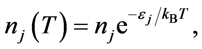 (21)
(21)
where  and 2 denote the “electron” and “hole”, respectively. The prefactor
  is the density at the high-temperature limit.
3. Phonons and Phonon Exchange Attraction
Phonons are bosons corresponding to the running normal modes of the lattice vibrations. They are characterized by the energy , where
  is the angular frequency, and the momentum vector
 , whose magnitude is
  times the wave numbers. The q-vector for phonons is similar to the k-vector for the conduction electrons. The phonon with
  represents a plane-wave proceeding in the
  -direction. The frequency
  is connected with the q-vector through the dispersion relation:
 (22)
(22)
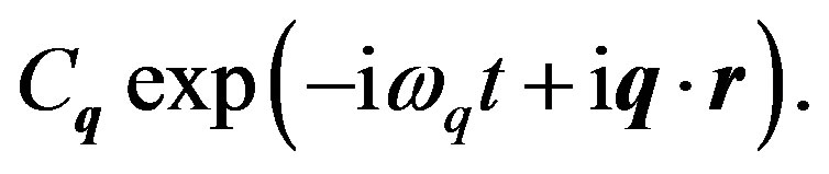
The excitation of the phonons can be discussed based on the same rectangular unit cell introduced for the conduction electrons. We note that phonons can be discussed naturally based on the orthogonal unit cells. [It is difficult to describe phonons in the WS cell model.] For example, longitudinal (transverse) phonons proceeding upwards are generated by imagining a set of plates each containing a number of rectangular cells executing small oscillations vertically (horizontally). A longitudinal wave proceeding in the crystal axis , is represented by
 (23)
(23)
where  is the displacement in the x-direction. If we imagine a set of parallel plates containing a great number of ions fixed in each plate, then we have a realistic picture of the lattice vibration mode. The density of ions changes in the x-direction. Hence, the longitudinal modes are also called the density-wave modes. The transverse wave mode can also be pictured by imagining a set of parallel plates containing a great number of ions fixed in each plate executing the transverse displacements. Notice that this mode generates no charge-density variation.
The Fermi velocity  in a typical metal is of the order
  while the speed of sound is of the order
 . The electrons are likely to move quickly to negate any electric field generated by the density variations associated with the lattice wave. In other words, the electrons may follow the lattice waves instantly. Given a traveling normal wave mode in Equation (21), we may assume an electron density variation of the form:
 (24)
(24)
Since electrons follow phonons immediately for all , the coefficient
  can be regarded as independent of
 . If we further assume that the deviation is linear in the scalar product
  and again in the electron density
 , we then obtain
 (25)
(25)
This is called the deformation potential approximation [15]. The dynamic response factor  is necessarily complex since the traveling wave is represented by the exponential form. Complex conjugation of Equation (24) yields
 . Using this form we can reformulate the electron’s response, but the physics must be the same. From this consideration, we obtain
 (26)
(26)
Each normal mode corresponds to a harmonic oscillator characterized by . The displacements
  can be expressed as
 (27)
(27)
where  are operators satisfying the Bose commutation rules:
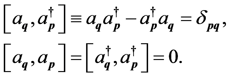 (28)
(28)
Let us now construct an interaction Hamiltonian , which has the dimensions of an energy and which is Hermitian. Using Equations (22) and (23), we obtain
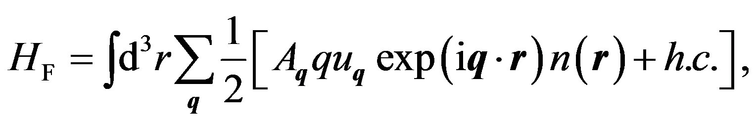 (29)
(29)
where h.c. denotes the Hermitian conjugate. This Hamiltonian  can be expressed as
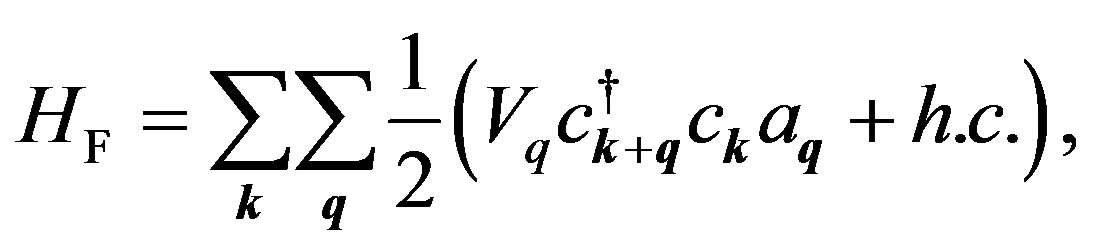 (30)
(30)
where , and
, and ,
,  are electron operators satisfying the Fermi anticommutation rules:
 (31)
(31)
The  in Equation (30) is the Fröhlich Hamiltonian [16]. In the process of deriving Equation (30), we found that the
  is applicable for the longitudinal phonons only. As noted earlier, the transverse lattice normal modes generate no charge density variations, making its contribution to
  negligible.
4. The Full Hamiltonian
Bardeen, Cooper and Schrieffer (BCS) published a historic theory of superconductivity in 1957 [17]. Following BCS, Fujita and his collaborators developed a quantum statistical theory of superconductivity in a series of papers [18-22]. Following this theory, we construct a generalized BCS Hamiltonian in this section.
In the ground state there are no currents for any system. To describe a supercurrent, we must introduce moving pairons, that is, pairons with finite center-of-mass (CM) momenta. Creation operators for “electron” (1) and “hole” (2) pairons are defined by
 (32)
(32)
We calculate the commutators among  and
and , and obtain
 (33)
(33)
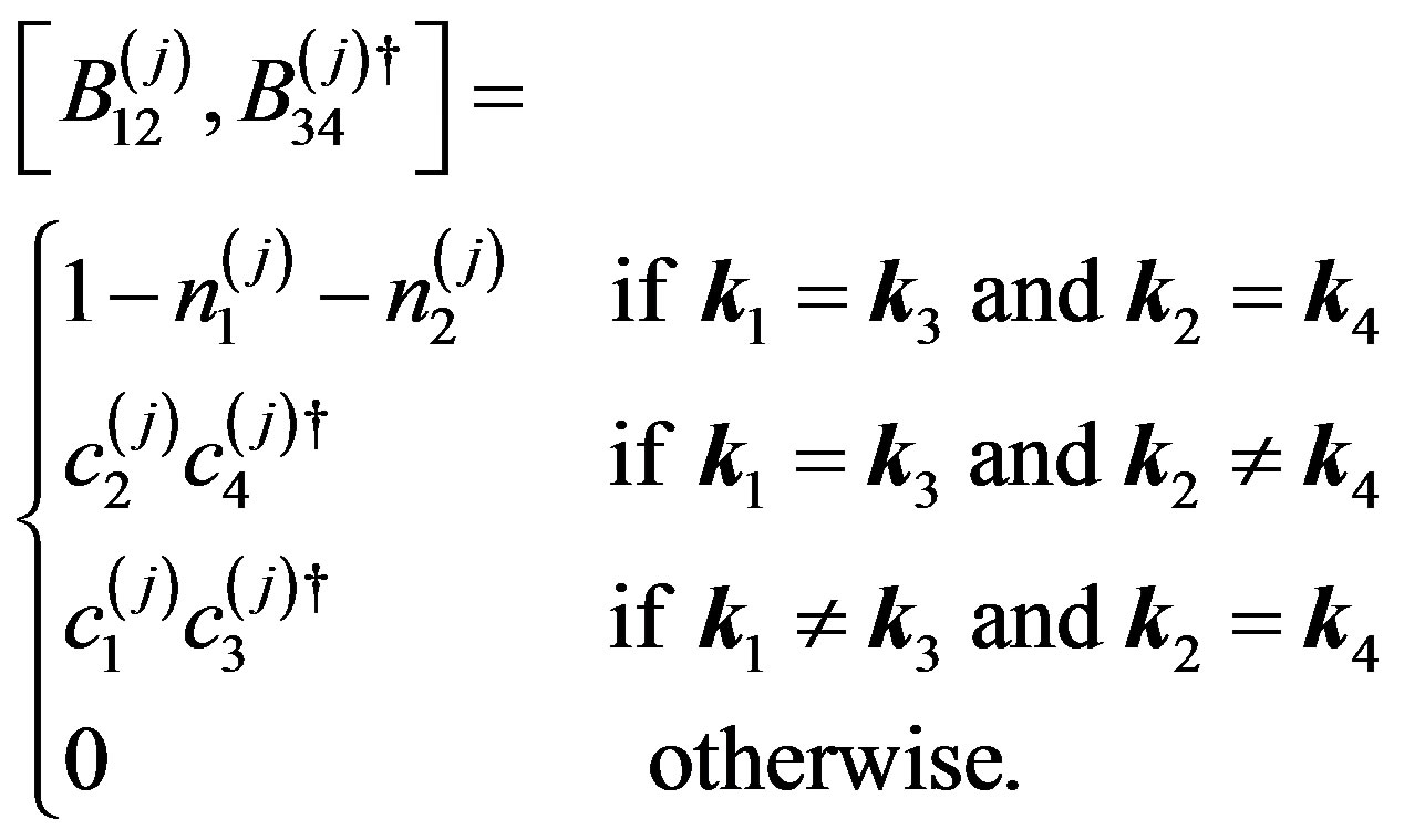 (34)
(34)
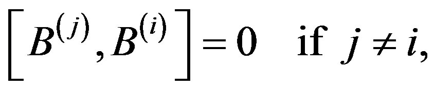
Pairon operators of different types  always commute:
 (35)
(35)
and
 (36)
(36)
represent the number operators for “electrons”  and “holes”
 .
.
Let us now introduce the relative and net momenta  such that
 (37)
(37)
Alternatively we can represent pairon annihilation operators by
 (38)
(38)
The prime on  will be dropped hereafter. In the k-q representation the commutation relations in Equations (33) and (34) are re-expressed as
 (39)
(39)
 (40)
(40)
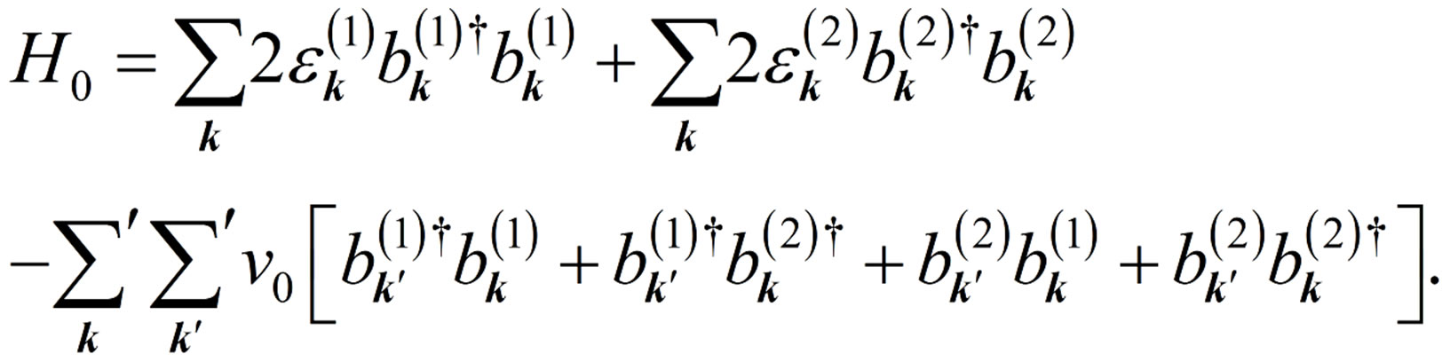
Using the new notations, we can write the full Hamiltonian as
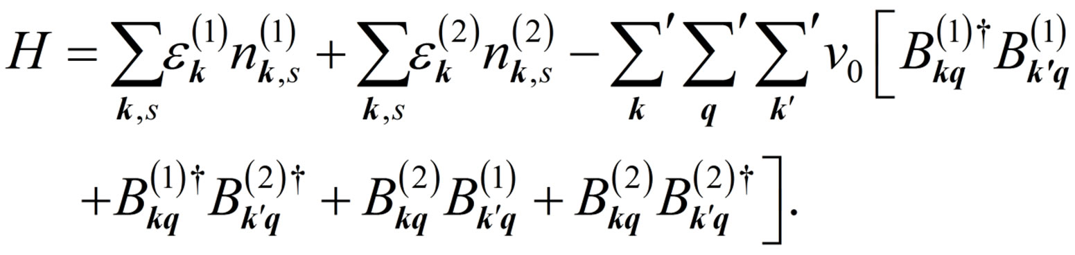 (41)
(41)
This is the full Hamiltonian for the system, which can describe moving pairons as well as stationary pairons. Here, the prime on the summations indicates the restriction arising from the phonon exchange attraction, see below. The connection with BCS Hamiltonian [17] will be discussed in Section 6.
5. Moving Pairons
The phonon exchange attraction is in action for any pair of electrons near the Fermi surface. In general the bound pair has a net momentum, and hence it moves. The energy  of a moving pairon can be obtained from:
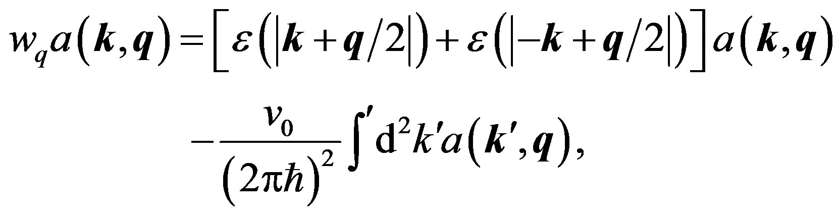 (42)
(42)
which is Cooper’s equation, Equation (1) of his 1956 Physical Review Letter [12]. The prime on the  - integral means the restriction on the integration domain arising from the phonon exchange attraction, see below. We note that the net momentum
  is a constant of motion, which arises from the fact that the phonon exchange attraction is an internal force, and hence cannot change the net momentum. The pair wavefunctions
  are coupled with respect to the other variable
 , meaning that the exact (or energy-eigenstate) pairon wavefunctions are superpositions of the pair wavefunctions
 .
.
Equation (42) can be solved as follows. We assume that the energy  is negative:
 (43)
(43)
Then,
 (44)
(44)
Rearranging the terms in Equation (1.42) and dividing by , we obtain
 (45)
(45)
where
 (46)
(46)
which is k-independent.
Introducing Equation (45) in Equation (42), and dropping the common factor , we obtain
 (47)
(47)
We now assume a free electron moving in 3D. The Fermi surface is a sphere of the radius (momentum)
 (48)
(48)
where  represents the effective mass of an electron. The energy
  is given by
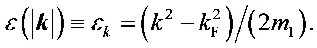 (49)
(49)
The prime on the  -integral in Equation (47) means the restriction:
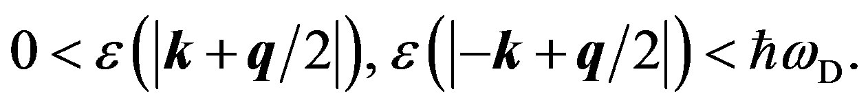 (50)
(50)
We may choose the polar axis along q as shown in Figure 5. The integration with respect to the azimuthal angle simply yields the factor . The
. The  -integral can then be expressed by
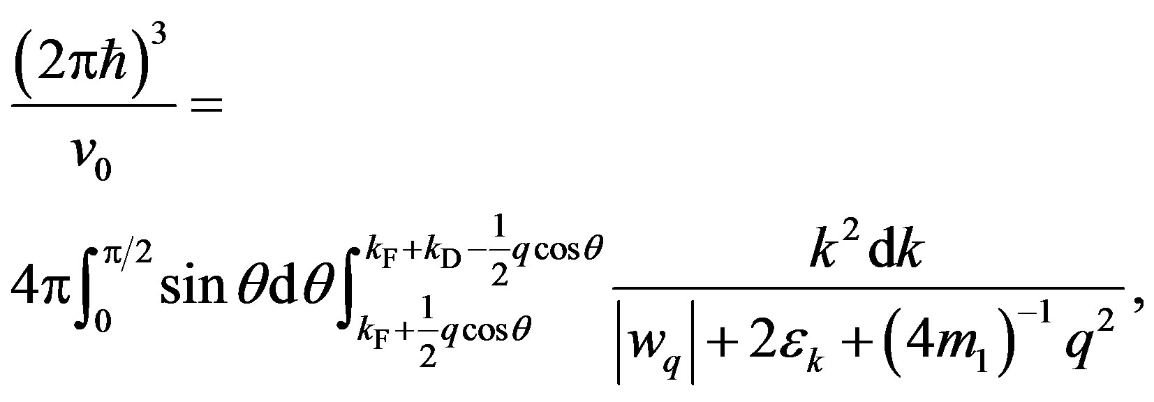 (51)
(51)
 (52)
(52)
After performing the integration and taking the small-q and small- limits, we obtain
 (53)
(53)
where the pairon ground-state energy  is given by
 (54)
(54)
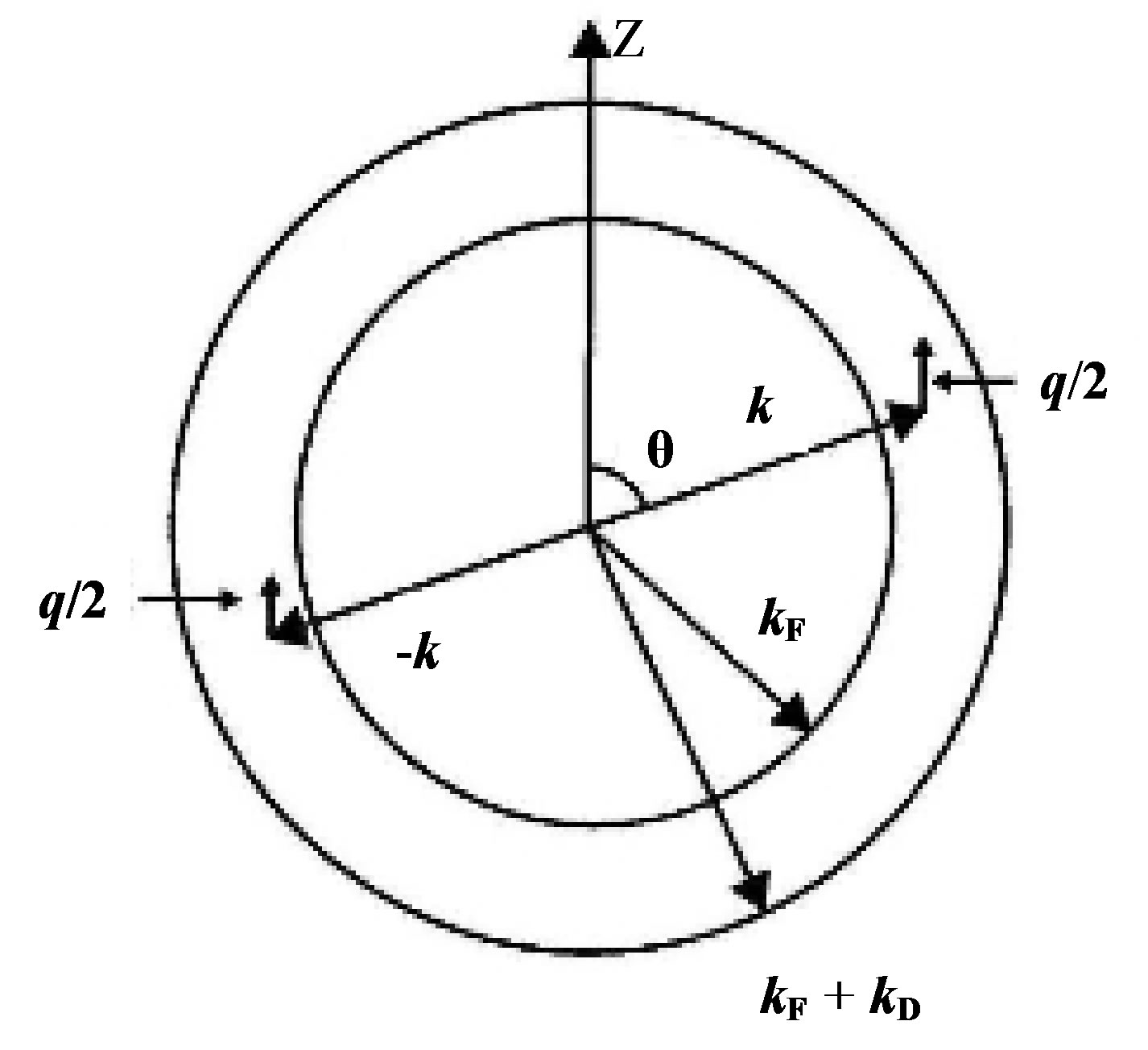
Figure 5. The range of the integration variables (k, θ) is limited to a spherical shell of thickness kD.
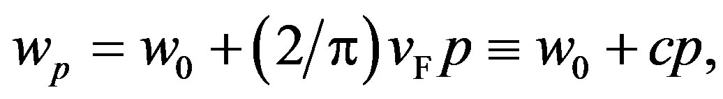
As expected, the zero-momentum pairon has the lowest energy . The excitation energy is continuous with no energy gap. Equation (53) was first obtained by Cooper (unpublished), and it is recorded in Schrieffer’s book [23], Equation (15). The energy
  increases linearly with momentum (magnitude)
  for small
 . This behavior arises from the fact that the density of states is strongly reduced with the increasing momentum
 , and dominates the
  increase of the kinetic energy. The linear dispersion relation means that a pairon moves likes a massless particle with a common speed
 . This relation plays a vital role in the B-E condensation of pairons (see next section).
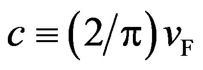
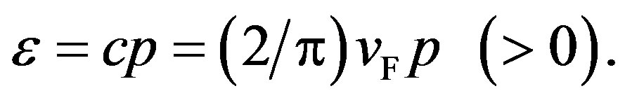
Such a linear energy-momentum relation is valid for pairons moving in any dimension (D). However, the coefficients slightly depend on the dimensions; in fact
 (55)
(55)
 and
and  for 3D and 2D, respectively.
6. The Bose-Einstein Condensation of Pairons
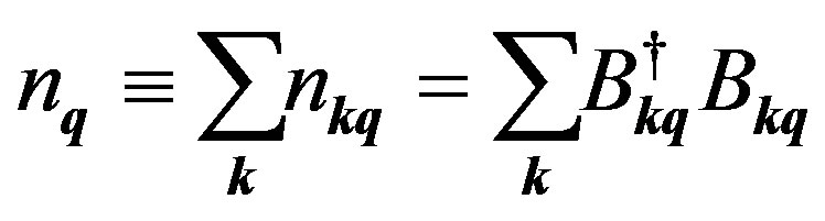
In Section 4, we saw that the pair operators 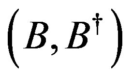 appearing in the full Hamiltonian
  in Equation (41) satisfy rather complicated commutator relations in Equations (39) and (40). In particular part of Equation (39)
 (56)
(56)
reflect the fermionic natures of the constituting electrons. Here,  represents creation operator for zero momentum pairons. BCS [17] studied the ground-state of a superconductor, starting with the reduced Hamiltonian
 , which is obtained from the Hamiltonian
  in Equation (41) by retaining the zero momentum pairons with
 , written in terms of
  by letting
  ,
,
 (57)
(57)
Here, we expressed the “electron” and “hole” kinetic energies in terms of pairon operators. The reduced Hamiltonian  is bilinear in pairon operators
 , and can be diagonalized exactly. BCS obtained the groundstate energy
  as
as
 (58)
(58)
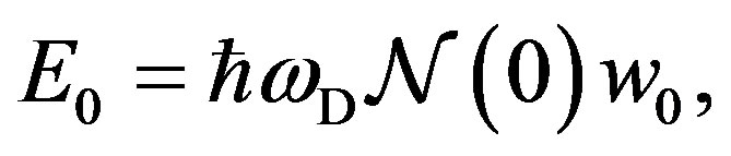
where 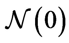 is the density of states at the Fermi energy. The
  is the ground-state energy of the pairon, see Equation (54). Equation (58) means simply that the ground state energy equals the numbers of pairons times the ground-state energy
  of the pairon. Our Hamiltonian
  in Equation (41) is reduced to the original BCS Hamiltonian (see Ref. [17], Equation (24)). There is an important difference in the definition of “electron” and “hole” here. BCS called the quasi-electron whose energy is higher (lower) than the Fermi energy
 , the “electron” (“hole”). In our theory the “electrons” (“holes”) are defined as quasiparticles generated above (below) the Fermi energy and circulates counterclockwise (clockwise) viewed from the tip of an external magnetic field vector
 . They are generated, depending on the energy contour curvature signs. For example, only “electrons” (“holes”) are generated for a circular Fermi surface with negative (positive) curvature whose inside (outside) is filled with electrons. Since the phonon has no charge, the phonon exchange cannot change the net charge. The pairing interaction terms in Equation (41) conserve the charge. The term
 , where
 ,
,  sample area, generates a transition in the “electron” states. Similarly, the exchange of a phonon generates a transition in the “hole” states, represented by
 . The phonon exchange can also pair-create or pair-annihilate “electron” (“hole”) pairons, and the effects of these processes are represented by
 ,
,  , as shown in Feynman diagrams in Figures 6(a) and (b). At 0 K the system must have equal numbers of – (+) zero-momentum (ground) pairons.
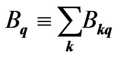
To describe a supercurrent, we must introduce moving pairons. We now show that the center-of-masses of the pairons move as bosons. That is, the number operator of pairons having net momentum 
 (59)
(59)
have the eigenvalues
 (60)
(60)
The number operator for the pairons in the state  is
is
 (61)
(61)
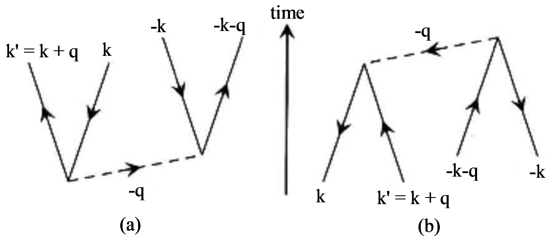
Figure 6. Feynman diagrams representing (a) pair-creation of ± ground pairons from the physical vacuum, and (b) pair annihilation. The time is measured upwards.
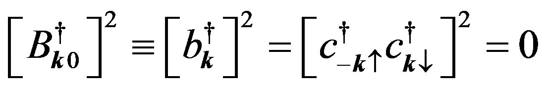
where we omitted the spin indices. Its eigenvalues are limited to zero or one:
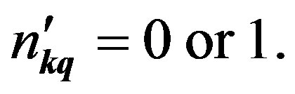 (62)
(62)
To explicitly see this property in Equation (60), we introduce
 (63)
(63)
and obtain
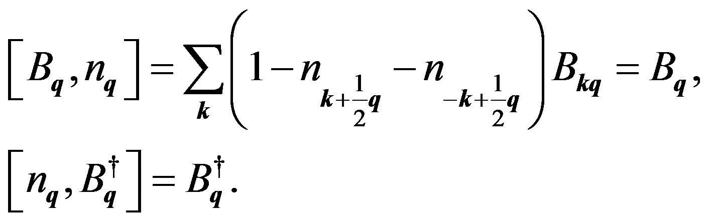 (64)
(64)
Although the occupation number  is not connected with
  as
as , the eigenvalues
  of
of  satisfying Equation (64) can be shown straightforwardly to yield [24]
 (65)
(65)
with the eigenstates
 (66)
(66)
In summary, pairons with both  and
and  specified are subject to the Pauli exclusion principle, see Equation (62). Yet, the occupation numbers
  of pairons having a CM momentum
  are
are .
.
The most important signature of many bosons is the Bose-Einstein Condensation (BEC). Earlier we showed that the pairon moves in 2D with the linear dispersion relation, see (53):
 (67)
(67)
where we designated the pairon net momentum (magnitude) by the more familiar  rather than
 .
.
Let us consider a 2D system of free bosons having a linear dispersion relation: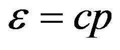 ,
, . The number of bosons,
  , and the Bose distribution function
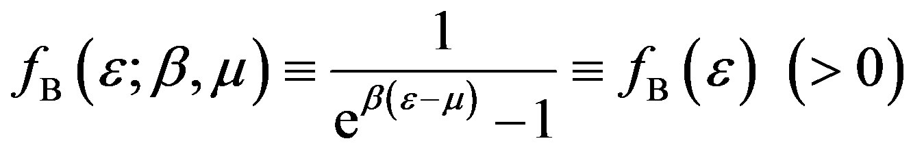 (68)
(68)
are related by
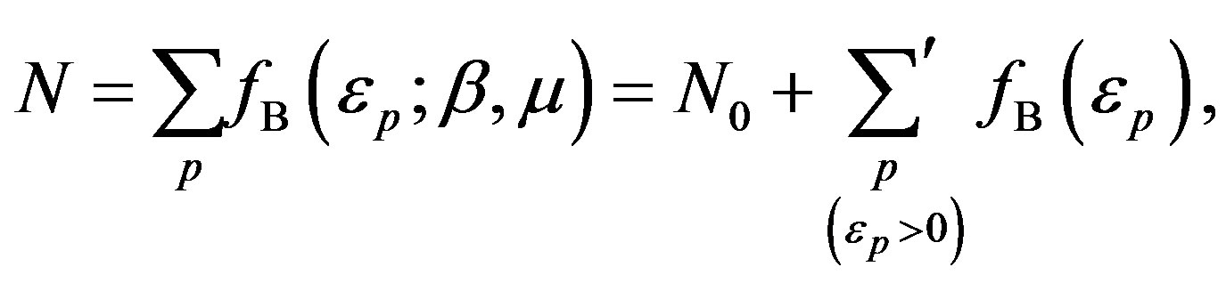 (69)
(69)
where  is the chemical potential,
 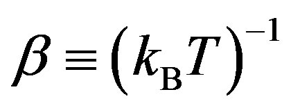 , and
, and
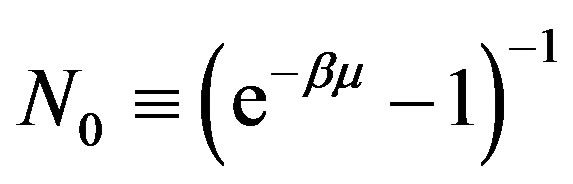 (70)
(70)
is the number of zero-momentum bosons. The prime on the summation in Equation (69) indicates the omission of the zero-momentum state. For notational convenience, we write
 (71)
(71)
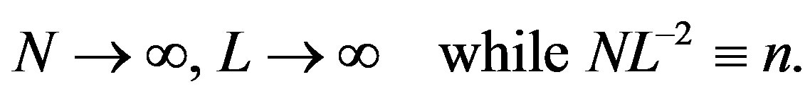
We divide Equation (69) by the normalization area , and take the bulk limit:
 (72)
(72)
We then obtain
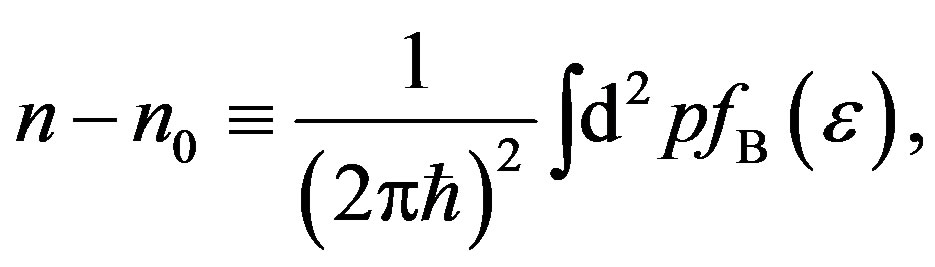 (73)
(73)
where 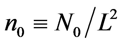 is the number density of zero-momentum bosons and
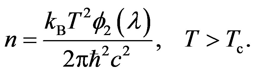
  the total boson density. After performing the angular integration and changing integration variables, we obtain from Equation (73):
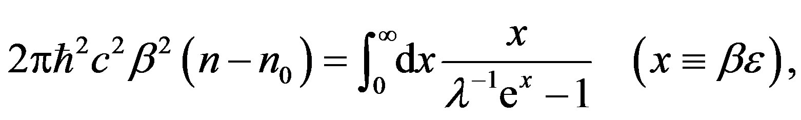 (74)
(74)
where the fugacity
 (75)
(75)
is less than unity for all temperatures. After expanding the integrand in Equation (74) in powers of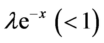 , and carrying out the x-integration, we obtain
 (76)
(76)
 (77)
(77)
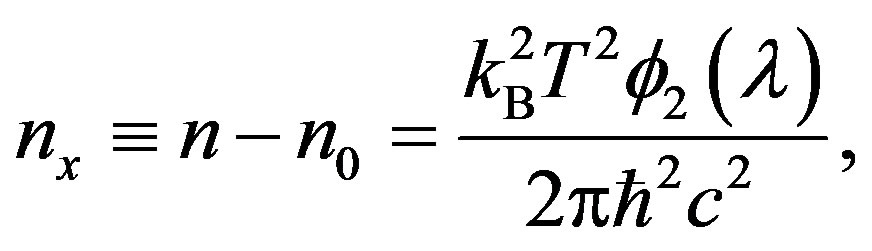
Equation (76) gives a relation among ,
,  , and
, and .
.
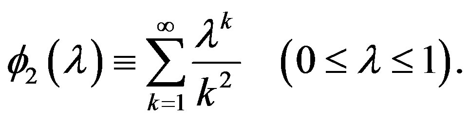
The function  monotonically increases from zero to the maximum value
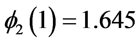 (78)
(78)
as  is raised from zero to one. In the low-temperature limit,
  ,
,  , and the density of excited bosons,
  , varies as
  as seen from Equation (76). This temperature behavior of
  persists as long as the right-hand-side (r.h.s.) of Equation (76) is smaller than
 ; the critical temperature
  occurs at
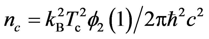 . Solving this, we obtain
 (79)
(79)
The BEC of pairons moving in 2D occurs at a finite temperature. This appears to contradict with Hohenberg’s theorem (no long range order in 2D). But this theorem is proved under the assumption of the f-sum rule arising from the mass conservation. The pairons move massless with the linear dispersion relation [see Equation (71)], and hence they are not subject to Hohenberg’s theorem [25].
If the temperature is raised beyond , the density of zero momentum bosons,
  , becomes vanishingly small, and the fugacity
  can be determined from
 (80)
(80)
In summary, the fugacity  is equal to unity in the condensed region:
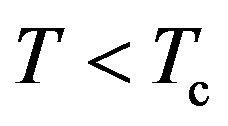 , and it becomes smaller than unity for
 , where its value is determined from Equation (80).
Formula (79) for the critical temperature  is distinct from the famous BCS formula
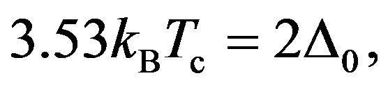 (81)
(81)
where  is the zero temperature electron energy gap in the weak coupling limit. The electron energy gap
  and the pairon ground-state energy
  both depend on the phonon-exchange coupling energy parameter
 , which appears in the starting Hamiltonian H in Equation (41). The energy
  is negative (bound-state energy). Hence, this
  cannot be obtained by the perturbation theory. The connection between
  and
and  is very complicated. This makes it difficult to discuss the critical temperature
  based on the BCS relation (81). Unlike the BCS formula, formula (79) is directly connected with the measurable quantities: the pairon density
  and the Fermi speed
 .
.
We emphasize here that both formulas (79) and (81) were derived, starting with the Hamiltonian  in Equation (41) and following statistical mechanical calculations, see the reference [27] for details.
7. Low Bias Anomaly
The unusual current-dips at zero bias in Figure 1 may be called the low bias anomaly (LBA). This effect is clearly seen in (a) low resistance contacts LRC sample. The differential conductance  increases with increasing bias, reaching a maximum at
 . With a further bias increase,
  drops dramatically. See (a), the upper panel in Figure 1. We will show that the LBA arises from the break-down of the superconducting state of the system.
With no bias, the nanotube’s wall below 150 K is in a superconducting state. If a small bias is applied, then the system is charged, positively or negatively depending on the polarity of the external bias. The applied bias field will not affect the neutral supercurrent but can accelerate the charges at the outer side of the carbon wall. The resulting normal currents carried by conduction electrons are scattered by impurities and phonons. The phonon population changes with temperature, and hence the phonon scattering is temperature-dependent. The normal electric currents along the tube length generate circulating magnetic fields, which eventually destroy the supercurrent running in the wall at a high enough bias. Thus, the current 
 versus the voltage
  (mV) is non-linear near the origin because of the supercurrents running in the wall. The differential conductance
  is very small and nearly constant (superconducting) for
  in the HRC sample, see the lower panel in Figure 1. We stress that if the ballistic electron model [2] is adopted, then the scatterings by phonons cannot be discussed. The non-linear
  curves below 150 K mean that the carbon wall is superconducting. Thus, the clearly visible temperature effects for both LRC and HRC samples arise from the phonon scattering. We assumed that the system is superconducting below
 . The LBA arises only from the superconducting state. The superconducting critical temperature
  must then be higher than 150 K. An experimental check of
  is highly desirable.
8. Temperature Behavior and Current Saturation
The high-bias I-V curves in Figure 3 is temperature-independent. This temperature behavior is consistent with our picture that the superconducting state of the metallic SWNT continued throughout the temperature range measured. Thus, the superconducting temperature  must be higher than 200 K.
The current saturation observed in Figure 3 may arise as follows. When the bias is raised from zero, the system will be charged with “holes” and the resulting “hole” currents run on the outer side of the tube, making an extra contribution to the current . The number of the running “holes” will grow as the bias voltage is raised. “Holes” obey the Fermi-Dirac statistics. At 0 K the number of “holes” is twice the number of the “hole” quantum states outside of the carbon wall, which is considerably smaller than the number of the orthogonal unit cells in the carbon wall. The number of the running “holes” cannot exceed twice the number of the quantum states because of Heisenberg’s uncertainty principle and Pauli’s exclusion principle. Thus, the “hole” current density calculated by
 (82)
(82)
must saturate to the maximum number  as the bias is raised further.
9. Summary
The unusual non-Ohmic transport behaviors at low (zero) bias anomaly, observed in metallic SWNT are explained in terms of a two-currents model. Supercurrents run in the graphene wall below 150 K. The normal “hole” currents on the outer-side of the tube are subject to scattering by phonons and impurities. The currents along the tube length generate circulating magnetic fields, which eventually destroy the supercurrent in the wall at high enough bias, and restore the Ohmic behavior. The lowcurrent anomaly is temperature-dependent since the phonon population changes with the temperature.
The I-V curves for the high bias (0.3 - 5 V) are temperature-independent (4 - 150 K), which arises from the fact that the neutral supercurrent running in the tube wall is not accelerated by the bias below the superconducting (critical) temperature. It is highly desirable to find the critical temperature by performing experiments above 150 K (experimental temperature).
The current saturation above 0.5 V observed arises from the limitation of the quantum-state sites for the “holes” running on the outer surface of the tube. If the tube’s circumference size is raised, then the saturation current should increase.
In the course of our calculations we uncover several significant facts as follows:
• To establish a 2D  -space for graphene we must introduce a rectangular unit cell distinct from the WS unit cell (rhombus).
• Electrons and phonons run anisotropically in graphene.
• Electrons and phonons are generated based on the same rectangular unit cells. This is important when dealing with the electron-phonon scattering and the phonon-exchange attraction.
• Phonons (bosonic quanta) representing the running plane-wave modes of the lattice oscillations are generated.
• The so-called Fröhlich interaction Hamiltonian  was derived, with the assumption that the electrons move in the perturbing density waves generated by the longitudinal phonons. The transverse phonons do not contribute to the Fröhlich interaction.
• “Electrons” and “holes” move as wave packets whose sizes are of the orthogonal unit cells.
• Phonons’ average size is much greater than the electron size. The average phonon energy is much smaller than the conduction electron energy.
• The BEC temperature for moving pairons is regarded as the superconducting temperature . Finding
  for metallic SWNT which is greater than 150 K from the studied experiments [1] is highly desirable.
REFERENCES
- Z. Yao, C. L. Kane and C. Dekker, Physical Review Letters, Vol. 84, 2000, pp. 2941-2944. doi:10.1103/PhysRevLett.84.2941
- R. Saito, G. Dresselhaus and M. S. Dresselhaus, “Physical Properties of Carbon Nanotubes,” Imperial College Press, London, 1998, pp. 35-39. doi:10.1142/9781860943799_0003
- S. Iijima, Nature, Vol. 354, 1991, pp. 56-58. doi:10.1038/354056a0
- E. Wigner and F. Seitz, Physical Review, Vol. 43, 1933, pp. 804-810. doi:10.1103/PhysRev.43.804
- S. Iijima and T. Ichihashi, Nature, Vol. 363, 1993, pp. 603-605. doi:1038/363603a0
- D. S. Bethune, et al., Nature, Vol. 363, 1993, pp. 605-607. doi:10.1038/363605a0
- S. Fujita, Y. Takato and A. Suzuki, Modern Physics Letters B, Vol. 25, 2011, pp. 223-242.
- S. Fujita, S. Godoy and A. Suzuki, Journal of Modern Physics, Vol. 3, 2012, pp. 1550-1555. doi:10.4236/jmp.2012.310191
- S. Moriyama, K. Toratani, D. Tsuya, M. Suzuki, Y. Aoyagi and K. Ishibashi, Physica E, Vol. 24, 2004, pp. 46-49. doi:10.1016/j.physe.2004.04.022
- S. J. Tans, M. H. Devoret, H. Dai, A. Thess, R. E. Smalley, L. J. Geerligs and C. Dekker, Nature, Vol. 386, 1997, pp. 474-477. doi:10.1038/386474a0
- S. J. Tans, A. R. M. Verschueren and C. Dekker, Nature, Vol. 393, 1998, pp. 49-52. doi:10.1038/29954
- L. N. Cooper, Physical Review, Vol. 104, 1956, pp. 1189- 1190. doi:10.1103/PhysRev.104.1189
- A. Bachtold, M. S. Fuhrer, S. Plyasunov, M. Forero, E. H. Anderson, A. Zettl and P. L. McEuen, Physical Review Letters, Vol. 84, 2000, pp. 6082-6085. doi:10.1103/PhysRevLett.84.6082
- N. W. Ashcroft and N. D. Mermin, “Solid State Physics,” Saunders, Philadelphia, 1976, pp. 228-229.
- W. A. Harrison, “Solid State Theory,” Dover, New York, 1980, pp. 390-393.
- H. Fröhlich, Physical Review, Vol. 79, 1950, pp. 845-856. doi:10.1103/PhysRev.79.845
- J. Bardeen, L. N. Cooper and J. R. Schrieffer, Physical Review, Vol. 108, 1957, pp. 1175-1204. doi:10.1103/PhysRev.108.1175
- S. Fujita, Journal of Superconductivity, Vol. 4, 1991, pp. 297-310. doi:10.1007/BF00618152
- S. Fujita, Journal of Superconductivity, Vol. 5, 1992, pp. 83-94. doi:10.1007/BF00618000
- S. Fujita and S. Watanabe, Journal of Superconductivity, Vol. 5, 1992, pp. 219-237. doi:10.1007/BF00617622
- S. Fujita and S. Watanabe, Journal of Superconductivity, Vol. 6, 1993, pp. 75-79. doi:10.1007/BF00617804
- S. Fujita and S. Godoy, Journal of Superconductivity, Vol. 6, 1993, pp. 373-379. doi:10.1007/BF00617974
- J. R. Schrieffer, “Theory of Superconductivity,” Benjamin, New York, 1964, p. 33.
- P. A. M. Dirac, “Principle of Quantum Mechanics,” 4th Edition, Oxford University Press, London, 1958, pp. 136- 138.
- P. C. Hohenberg, Physical Review, Vol. 158, 1967, pp. 383-386. doi:10.1103/PhysRev.158.383
- N. D. Mermin and H. Wagner, Physical Review Letters, Vol. 17, 1966, pp. 1133-1136. doi:10.1103/PhysRevLett.17.1133
- S. Fujita, K. Ito and S. Godoy, “Quantum Theory of Conducting Matter: Superconductivity,” Springer, New York, 2009, pp. 79-81. doi:10.1007/978-0-387-88211-6