Paper Menu >>
Journal Menu >>
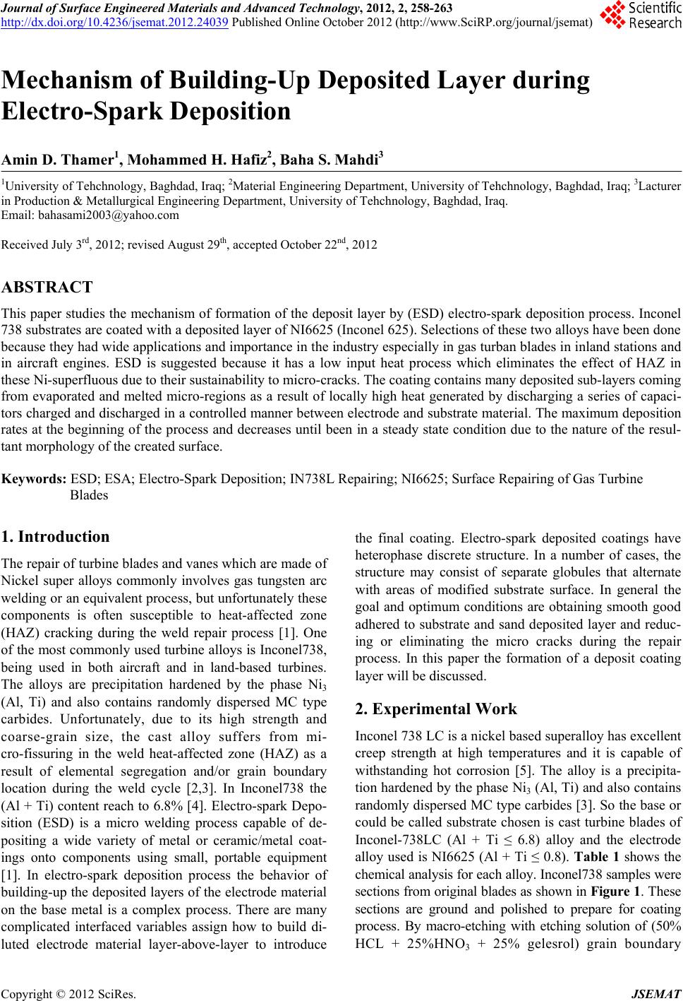 Journal of Surface Engineered Materials and Advanced Technology, 2012, 2, 258-263 http://dx.doi.org/10.4236/jsemat.2012.24039 Published Online October 2012 (http://www.SciRP.org/journal/jsemat) Mechanism of Building-Up Deposited Layer during Electro-Spark Deposition Amin D. Thamer1, Mohammed H. Hafiz2, Baha S. Mahdi3 1University of Tehchnology, Baghdad, Iraq; 2Material Engineering Department, University of Tehchnology, Baghdad, Iraq; 3Lacturer in Production & Metallurgical Engineering Department, University of Tehchnology, Baghdad, Iraq. Email: bahasami2003@yahoo.com Received July 3rd, 2012; revised August 29th, accepted October 22nd, 2012 ABSTRACT This paper studies the mechanism of formation of the deposit layer by (ESD) electro-spark deposition process. Inconel 738 substrates are coated with a deposited layer of NI6625 (Inconel 625). Selections of these two alloys have been done because they had wide applications and importance in the industry especially in gas turban blades in inland stations and in aircraft engines. ESD is suggested because it has a low input heat process which eliminates the effect of HAZ in these Ni-superfluous due to their sustainability to micro-cracks. The coating contains many deposited sub-layers coming from evaporated and melted micro-regions as a result of locally high heat generated by discharging a series of capaci- tors charged and discharged in a controlled manner between electrode and substrate material. The maximum deposition rates at the beginning of the process and decreases until been in a steady state condition due to the nature of the resul- tant morphology of the created surface. Keywords: ESD; ESA; Electro-Spark Deposition; IN738L Repairing; NI6625; Surface Repairing of Gas Turbine Blades 1. Introduction The repair of turbine blades and vanes which are made of Nickel super alloys commonly involves gas tungsten arc welding or an equivalent process, but unfortunately these components is often susceptible to heat-affected zone (HAZ) cracking during the weld repair process [1]. One of the most commonly used turbine alloys is Inconel738, being used in both aircraft and in land-based turbines. The alloys are precipitation hardened by the phase Ni3 (Al, Ti) and also contains randomly dispersed MC type carbides. Unfortunately, due to its high strength and coarse-grain size, the cast alloy suffers from mi- cro-fissuring in the weld heat-affected zone (HAZ) as a result of elemental segregation and/or grain boundary location during the weld cycle [2,3]. In Inconel738 the (Al + Ti) content reach to 6.8% [4]. Electro-spark Depo- sition (ESD) is a micro welding process capable of de- positing a wide variety of metal or ceramic/metal coat- ings onto components using small, portable equipment [1]. In electro-spark deposition process the behavior of building-up the deposited layers of the electrode material on the base metal is a complex process. There are many complicated interfaced variables assign how to build di- luted electrode material layer-above-layer to introduce the final coating. Electro-spark deposited coatings have heterophase discrete structure. In a number of cases, the structure may consist of separate globules that alternate with areas of modified substrate surface. In general the goal and optimum conditions are obtaining smooth good adhered to substrate and sand deposited layer and reduc- ing or eliminating the micro cracks during the repair process. In this paper the formation of a deposit coating layer will be discussed. 2. Experimental Work Inconel 738 LC is a nickel based superalloy has excellent creep strength at high temperatures and it is capable of withstanding hot corrosion [5]. The alloy is a precipita- tion hardened by the phase Ni3 (Al, Ti) and also contains randomly dispersed MC type carbides [3]. So the base or could be called substrate chosen is cast turbine blades of Inconel-738LC (Al + Ti ≤ 6.8) alloy and the electrode alloy used is NI6625 (Al + Ti ≤ 0.8). Table 1 shows the chemical analysis for each alloy. Inconel738 samples were sections from original blades as shown in Figure 1. These sections are ground and polished to prepare for coating process. By macro-etching with etching solution of (50% HCL + 25%HNO3 + 25% gelesrol) grain boundary Copyright © 2012 SciRes. JSEMAT  Mechanism of Building-Up Deposited Layer During Electro-Spark Deposition 259 Figure 1. Sectione d and macro-etched spe cimen (5×). Table 1. Nominal composition of IN738 [5]. Inconel 738 NI6625 Element wt% Element wt% Ni Bal. Ni Bal. Cr 15.84 Cr 21.0 Co 8.5 Co 0.0 Mo 1.88 Mo 9.0 W 2.48 W 0.0 Nb 0.92 Nb 3.5 Al 3.46 Al 0.0 Ti 3.47 Ti + Fe 0.07 Fe 5.0 Ta 1.69 Ta 0.0 C 0.11 C 0.04 B 0.012 B 0.0 Zr 0.04 Mn 0.4 S 0.001 Si 0.7 revealed as shown in Figure 1. The grains were coarse (4.6 mm means grain size). Electrode alloy Inconel 625 or (NI6625) was as welding electrodes with a diameter of (3.2) mm and coated with a flux. The flux was removed and the wire was cleaned by coarse and fine grinding papers to remove any remained flux on it, then they are divided for the intended length. The electrode is fixed with a rotating head of a DC elec- tric motor and the rotating speed is varying from 0 to 1200 RPM. Electro-spark deposition machine is manu- factured with ability of varying voltage analogy from 0 - 120 Volt and frequency with (50-100-200-300-400-500- 600-700-800) Hz with a fixed capacitance of 50 μf. Ar- gon inert gas is used also as a shielded gas to prevent oxidation during the process. 3. Results and Discussion First with ESD process variables of 25 Volt, 400 Hz and rotating electrode of 600 RPM using argon a track line of deposition are built along the width of the substrate specimen as shown in Figure 2 which represents image taken by using electron scanning microscope. From Figure 2, it is easy to divide the surface to three regions: the first is called the near region which is elec- trode vapor effected area in the two sides of the track; it’s shown as white areas, in this region a vapor and some melted electrode-substrate material splashed due to dis- charging during instantaneously contact between the electrode and substrate. These small amounts of splash- ing alloy solidify rapidly in the moment of contact with the substrate and its chemical composition depend on some factors such the stage of the deposition layer, con- tact pressure, electrode rotation speed and the two mate- rial thermal properties. Region (1) is important because it will be contacted and discharged later to make another primary coating layer so it increases the dilution elec- trode percentage, oxidation in the above (later) deposited layers. Figure 3 shows a clear shape to the region (1). From Figure 3 it can be understood every splashed so- lidified arrow represented in the opposite direction to the center of the discharge single spark for every arrow di- rection, so the variation of arrow direction indicates that the region suffered from contaminating by a large num- ber of flying melted small droplets. Under solidified droplets it can be seen a porous surface with a less than 2 μm diameter holes. These holes are the results of solidified vapor on sur- face resulted from the discharging process because they were not found in the substrate as polished alloy. The maximum distance of the region (1) far away from melted regions was 200 - 400 μm which represents the maximum distance a droplet can be flown in melted con- ditions before they solidify in the air and go far away. Region (2) not appear in all ESD process of full surface coating but it is founded here to explain how does over- lap can be done by changing the distance during move- ment of electrode with multiple discharging operations. Figure 4 explain region (2) clearly. From Figure 4 it can be easily counted the multiple stages with careful which were six overlapped layers as shown above. Overlap percentage cannot be specified easily by the manual ESD process because it depends on the liner movement speed of the electrode respect to the substrate, at the above image it can be 80% - 90% over- lap between multiple sparks. Small holes and arrows can be seen also in a primary stage of discharging and de- crease during transportation to newer layers. If the discharging frequency is low and linear move- ment is high it may be no overlapping as shown in Fig- ure 5 below when the frequency was (50 Hz), voltage was (100 Volt) and electrode rotating speed was 800 RPM. Minimum overlapping can produce more porous de- posited coating and this lead to weakness and increases Copyright © 2012 SciRes. JSEMAT 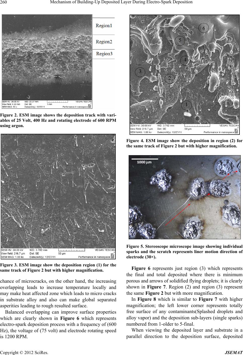 Mechanism of Building-Up Deposited Layer During Electro-Spark Deposition 260 Figure 2. ESM image shows the deposition track with vari- ables of 25 Volt, 400 Hz and rotating electrode of 600 RPM using argon. Figure 3. ESM image show the deposition region (1) for the same track of Figure 2 but with higher magnification. chance of microcracks, on the other hand, the increasing overlapping leads to increase temperature locally and may make heat affected zone which leads to micro cracks in substrate alloy and also can make global separated asperities leading to rough resulted surface. Balanced overlapping can improve surface properties which are clearly shown in Figure 6 which represents electro-spark deposition process with a frequency of (600 Hz), the voltage of (75 volt) and electrode rotating speed is 1200 RPM. Figure 4. ESM image show the deposition in region (2) for the same track of Figure 2 but with higher magnification. Figure 5. Stereoscope microscope image showing individual sparks and the scratch represents liner motion direction of electrode (30×). Figure 6 represents just region (3) which represents the final and total deposited where there is minimum porous and arrows of solidified flying droplets; it is clearly shown in Figure 7. Region (2) and region (3) represent the same Figure 2 but with more magnification. In Figure 8 which is similar to Figure 7 with higher magnification; the left lower corner represents totally free surface of any contaminants(Splashed droplets and alloy vapor) and the deposition sub-layers (single sparks) numbered from 1-older to 5-final. When viewing the deposited layer and substrate in a parallel direction to the deposition surface, deposited Copyright © 2012 SciRes. JSEMAT  Mechanism of Building-Up Deposited Layer During Electro-Spark Deposition 261 Figure 6. Stereoscopic microscope image showing complet- ed coated surface of IN738 by IN625 (25×). Figure 7. ESM image show the deposition in regions (2) & (3) for the same track of Figure 2 but with magnification (100×). Figure 8. ESM image show the deposition in region (3) which is similar to image (7) but with magnification (500×). specimens are sectioned-mounted-grind-polished and etch- ed by immersion in etching solution of (50% HCL + 25%HNO3 + 25% gelesrol) for 40 second. Resultant of that Figure 9 shows the interface between the coating and substrate alloy with ESD of 100 Volt and 800 Hz, the deposition is sound from inclusions and gaps or cracks same for the substrate which is free of microcracks, that’s indicated there is a very little heat generated from the process. From Figure 9 it can be seen a rough outside surface, and the mean coating thickness was 73 μm. Figure 10 explain a single spark effect on the surface making like an arc shape bowed forward the depth in substrate alloy and the region (d) can be considered the maximum diluted electrode material by substrate alloy for the second sub-layer caused by second spark. So from all that the spark effect can be simplified in shape as a representative drawing in Figure 11. Figure 9. EPType2 Metallurgical microscope image show the interface between coating and substrate alloy with ESD of 100 Volt and 800 Hz (300×). Figure 10. EPType2 Metallurgical microscope image show the interface layer between coating and substrate alloy with ESD of 100 Volt and 800 Hz (600×). Copyright © 2012 SciRes. JSEMAT  Mechanism of Building-Up Deposited Layer During Electro-Spark Deposition 262 At contact and beginning of the first spark formed due to discharging high local heat generated between elec- trode and substrate, electrode moves and rotates at the same time so there is no chance to make a static junction between them. Due to the spherical shape of electrode and positive polarity, temperature will rise rapidly evaporate and melt it more than the substrate which has negative polarity and flat so it is melted and evaporated in less amount than the electrode also heat is dissipated in substrate quicker than the electrode. Returning to Fig- ure 11(a) discharge generates heat which evaporates and expands the volume rapidly making very high local pressure; therefore, liquid pool will splash to surrounding circumstances and solidify because of absorbed heat by lower substrate, some vapor and flying droplets solidify in near area which is called a region (1) and some of them solidify in the air and go away. Center of the pool will be less in height than the original substrate because of splashing and it contains high amount of electrode material (60%) and (40%) of the substrate material that is similar for the splashed surrounding the pole but its height is more than the original substrate in (5 - 15) μm so it’s the major parameter in building coating in the process. Heat of second discharging evaporates and melts primer material deposited in the first spark with very little amount of the substrate and alloyed with the new melted electrode material which is diluted by the old de- posited layer; therefore, the new material (Green in drawing) contains 60% of electrode and 40% of the prier deposited layer. Figure 11(b) explains second spark gen- erated during movement of the electrode toward the left. Increase in deposition thickness in second spark is less than the first which will appear in the back direction of movement as explained in graph in 3 - 5 μm for each pass. That low increase in multi-passes are caused also by changing the shape of the substrate at later pass and it will not be flat, it has asperities of deposit layer when it is contrasted with electrode, the heat generated will melt the larger amount of it than the prier flat substrate mate- rial. That leads to decrease deposition rate of electrode (b) (a) region (1) region (2) region (3) electrode movement direction Figure 11. Representative resultant material distribution at single spark (a) and the second ove rlapped spark. Substr ate (Blue), first spark material formation (Red), second spark material formation (Green). material with respect to the first flat areas of the substrate. Figure 12 shows eight multiple sparks at a total distance of 4 mm with (40% - 60%) overlapping, so it can be seen that the shape of spots is not easy as model assumptions in Figure 11 but the representation was made to facilitate approximations and that assumption was right. Figure 13 shows the real single spark by applying (100 Volt, 50 Hz and 400 RPM of electrode) without using argon as inert gas therefore it can be seen that there is no evaporated effect around spark circumstances and the ends of solidified droplet black in color because of oxidation. During multi-passes the deposition rate will be in steady state but remains less than the first layers depos- ited. Therefore dilution of substrate in depositing layer is found to be narrow region near the original substrate in several microns. Figure 14 Shows starting (a) and maximum (b) dis- charging power and it can be seen easily that the tip of the electrode takes a cone shape depending on the angle of contact between the surface of substrate and the elec- trode rotation axis. 4. Conclusions 1) When analyzing the deposited surface by electro- spark deposition process there are three main regions. Region (1) and region (2) responsible for the amount of alloying (dilution) of the electrode material by the sub- Figure 12. Shows eight sparks viewed from right to left which is the electrode liner movement direction. Figure 13. Stereoscope microscope image showing individ- ual spark with process parameters of (100 Volt, 50 Hz and 400 RPM of electrode) (90×). Copyright © 2012 SciRes. JSEMAT  Mechanism of Building-Up Deposited Layer During Electro-Spark Deposition Copyright © 2012 SciRes. JSEMAT 263 understand the mechanism of deposition point by point. (a) (b) 2) Applying line and probe analysis through deposited and base metal to know how the base and filler material elements distributed. REFERENCES Figure 14. Show starting (a) and maximum (b) discharging power during continues ESD process. [1] U.S. Department of Defense, “Electrospark Deposition for Depot- and Field-Level Component Repair and Re- placement of Hard Chromium Plating,” Environmental Security Technology Certification Program (ESTCP), Alexandria, 2006. strate alloy these regions are affected by the process variables and the second region is reduced or eliminated when complete surface coating occur. Overall coating thickness includes multi-sub layers caused by individual discharged sparks every one of them adds some thickness to the coating but remains less than the first layer added at the beginning of the process. [2] A. Thakur, N. L. Richards and M. C. Chaturvedi, “On Crack-Free Welding of Cast Inconel 738,” International Journal for the Joining of Materials, Vol. 15, No. 4, 2003, pp. 21-25. [3] K. Banerjee, N. L. Richards and M. C. Chaturvedi, “Ef- fect of Filler Alloys on HAZ Cracking in Pre-Weld Heat Treated IN-738 LC GTA Welds, Metallurgical and Ma- terials Transactions A, Vol. 36, No. 7, 2005, pp. 1881- 1890. 2) The complex shape of sparks can be simplified as a circular pool surrounded by splashing solidified diluted mixture alloy of substrate and electrode alloy followed by region (1) of evaporated and flying melted droplets. 3) Maximum dilution concentration occurs in the dis- tance above the substrate in about 1 - 2 μm and in some cases reach to 5 μm. [4] J. Durocher and N. L. Richards, “Evaluation of the Low Heat Input Process for Weld Repair of Nickel-Base Super- alloys,” Journal of Materials Engineering and Perform- ance, Vol. 20, No. 7, 2011, pp. 1294-1303. [5] R. C. Reed, “The Superalloys Fundamentals and Applica- tions,” Cambridge University Press, Cambridge, 2006, p. 23. 5. Recommendations 1) Study the possibility of high-speed video imaging to |