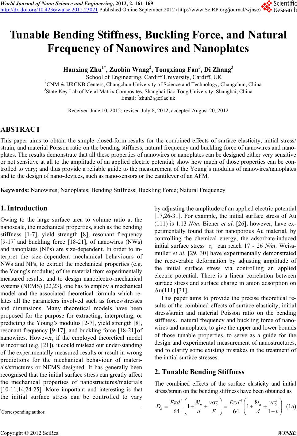
 World Journal of Nano Science and Engineering, 2012, 2, 161-169 http://dx.doi.org/10.4236/wjnse.2012.23021 Published Online September 2012 (http://www.SciRP.org/journal/wjnse) Tunable Bending Stiffness, Buckling Force, and Natural Frequency of Nanowires and Nanoplates Hanxing Zhu1*, Zuobin Wang2, Tongxiang Fan3, Di Zhang3 1School of Engineering, Cardiff University, Cardiff, UK 2CNM & IJRCNB Centers, Changchun University of Science and Technology, Changchun, China 3State Key Lab of Metal Matrix Composites, Shanghai Jiao Tong University, Shanghai, China Email: *zhuh3@cf.ac.uk Received June 10, 2012; revised July 8, 2012; accepted August 20, 2012 ABSTRACT This paper aims to obtain the simple closed-form results for the combined effects of surface elasticity, initial stress/ strain, and material Poisson ratio on the bending stiffness, natural frequency and buckling force of nanowires and nano- plates. The results demonstrate that all these properties of nanowires or nanoplates can be designed either very sensitive or not sensitive at all to the amplitude of an applied electric potential; show how much of those properties can be con- trolled to vary; and thus provide a reliable guide to the measurement of the Young’s modulus of nanowires/nanoplates and to the design of nano-devices, such as nano-sensors or the cantilever of an AFM. Keywords: Nanowires; Nanoplates; Bending Stiffness; Buckling Force; Natural Frequency 1. Introduction Owing to the large surface area to volume ratio at the nanoscale, the mechanical properties, such as the bending stiffness [1-7], yield strength [8], resonant frequency [9-17] and buckling force [18-21], of nanowires (NWs) and nanoplates (NPs) are size-dependent. In order to in- terpret the size-dependent mechanical behaviours of NWs and NPs, to extract the mechanical properties (e.g. the Young’s modulus) of the material from experimentally measured results, and to design nanoelectro-mechanical systems (NEMS) [22,23], one has to employ a mechanical model and the associated theoretical formula which re- lates all the parameters involved such as forces/stresses and dimensions. Many theoretical models have been proposed for the purpose for extracting, interpreting, or predicting the Young’s modulus [2-7], yield strength [8], resonant frequency [9-17], and buckling force [18-21] of nanowires. However, if the employed theoretical model is incorrect (e.g. [21]), it could mislead our under-standing of the experimentally measured results or result in wrong predictions for the mechanical behaviour of materi- als/structures or NEMS designed. It has generally been recognised that the initial surface stress can greatly affect the mechanical properties of nanostructures/materials [10-11,14,24-25]. More important and interesting is that the initial surface stress can be controlled to vary by adjusting the amplitude of an applied electric potential [17,26-31]. For example, the initial surface stress of Au (111) is 1.13 N/m. Biener et al. [26], however, have ex- perimentally found that for nanoporous Au material, by controlling the chemical energy, the adsorbate-induced initial surface stress 0 can reach 17 - 26 N/m. Weiss- muller et al. [29, 30] have experimentally demonstrated the recoverable deformation by adjusting amplitude of the initial surface stress via controlling an applied electric potential. There is a linear correlation between surface stress and surface charge in anion adsorption on Au(111) [31]. This paper aims to provide the precise theoretical re- sults of the combined effects of surface elasticity, initial stress/strain and material Poisson ratio on the bending stiffness,natural frequency and buckling force of nano- wires and nanoplates, to give the upper and lower bounds of those tunable properties, to serve as a guide for the design and experimental measurement of nanostructures, and to clarify some existing mistakes in the treatment of the initial surface stresses. 2. Tunable Bending Stiffness The combined effects of the surface elasticity and initial stress/strain on the bending stiffness have been obtained as 44 00 88 ππ 11 6464 1 xx nn b lv lv Ed Ed DdEd v (1a) *Corresponding author. C opyright © 2012 SciRes. WJNSE  H. X. ZHU ET AL. 162 for nanowires with a circular cross-section [24], 0.1E 4 4 1 12 1 12 bEd D Ed 0 0 83 2 83 2 1 x n x n lv dE lv dv (1b) or 4 4 1 12 1 12 bEd D Ed 0 0 42 42 1 x n x n lv dE lv dv /lSE (1c) for nanowires with a square cross-section [25] when bending is about a neutral plane parallel to the surface plane (1b) or about a diagonal plane (1c). Where, d is the cross-sectional diameter in Equation (1a) or the side length of the square cross-section in Equations (1b) and (1c); E is the Young’s modulus of the bulk material; n is the intrinsic length of the material at the nano scale; and S is the surface elasticity modulus. In order to simplify the analysis and results, both the sur- face and the bulk materials are assumed to be isotropic and to have the same Poisson ratio v; the initial surface stresses in both the axial and the circular directions are assumed to be the same as 0 . The initial residual stress of the bulk material in the axial direction of the nanowire with either a circular or a square cross-section is thus 00 because equilibrium in the axial direction has to be held for a free nanowire such as a cantilever. For a uniform nanowire with either a circular or a square cross-section, the initial stresses in the bulk material in both the radial and the circular directions are half of that in the axial direction, i.e. 000 0 . The initial residual elastic strain in the axial direction, 0, of a nanowire is related to the initial surface stresses by 00 . The von Mises stress of the bulk material should not exceed the material yield strength 4/ xd /22 /d x rx )/()Edv1( 4 x , otherwise, the nanowire would undergo permanent plastic deformation. Atomistic simulation [32] has shown that if the diameter of a gold wire is suffi- ciently small, it can automatically undergo plastic de- formation solely owing to the presence of the initial sur- face stresses. It is well known that the yield strength, , of some conductive polymer materials or nano-sized me- tallic materials can be (E is the Young’s modulus) or larger [33]. Biener et al. [26] have experimentally found that for nanoporous Au material, by controlling the chemical energy, the adsorbate-induced surface stress 0 E1.0 can reach 17 - 26 N/m. If the diameter of the liga- ments is 5 nm, 0 would be 20 GPa. As the bulk mate- rial discussed in this paper can be either metallic, or polymeric or biological, without losing generality, the von Mises yield strength is assumed to be y . If the actual yield strength of the bulk material of a nanowire/nanoplate is larger or smaller than , its tunable ranges of the bending stiffness, natural frequency, and axial compressive buckling force can still be ob- tained by scaling up or scaling down the results that are presented in sections that follow. E1.0 According to the aforementioned assumptions, for recoverable elastic deformation, the amplitude of the von Mises stress in the bulk material of a nanowire is limited by 0ey . The corresponding initial strain in the axial direction is 00 . The strain in the radial direction of the nanowire cross-section is related to the initial surface stresses or the initial re- sidual elastic strain in the axial direction by /2 0.1 xE 1/ xxvE 00 00 213 13 13 221 x rx v vv Ed Ev (2) when the effects of both the surface elasticity and the initial surface stress 0 are absent (i.e. n and 0000 0Sl xxr d 4 00 π/64DdE 4/12DdE 0 0), the diameter or side-length of the cross-section of a nanowire is assumed to be 0 and the corresponding conventional bending stiffness to be for a circular cross-section or 00 for a square cross-section. When the ef- fect of the initial surface stresses is present, 000 0 13 11 21 rx v dddv (3) Substituting Equation (3) into (1a), the combined ef- fects of the surface elasticity and initial stresses on the bending stiffness of a nanowire with a circular cross- section can be obtained as 4 0 0 0 813 11 121 xx bn Dlv v Ddvv /0 n ld (4) when the effect of the surface modulus S is absent (i.e. 0 or 0n d), the effect of the initial stress 0 l on the dimensionless bending stiffness 0b of a nanowire with a circular cross-section is plotted against the possible value of the Poisson ratio v of the bulk mate- rial for different amplitudes of the initial stress: 0 /DD x 0.2E, 0.1E, 0, −0.1E, −0.2E (note that the corre- sponding von Mises stresses are e /DD 0.1E, 0.05E, 0, 0.05E and 0.1E, respectively), as shown in Figure 1(a). As can be seen from Figure 1(a), when the Poisson ratio of the bulk material v is close to 0, the normalised bend- ing stiffness, 0b, of a nanowire can be controlled to vary over a range from 0.65 to 1.4 by adjusting the am- plitude of the initial stress 0 from −0.2E to 0.2E (this, in turn, can be realised by adjusting the amplitude of an applied electric potential). The tunable range of 0 / b DD Copyright © 2012 SciRes. WJNSE 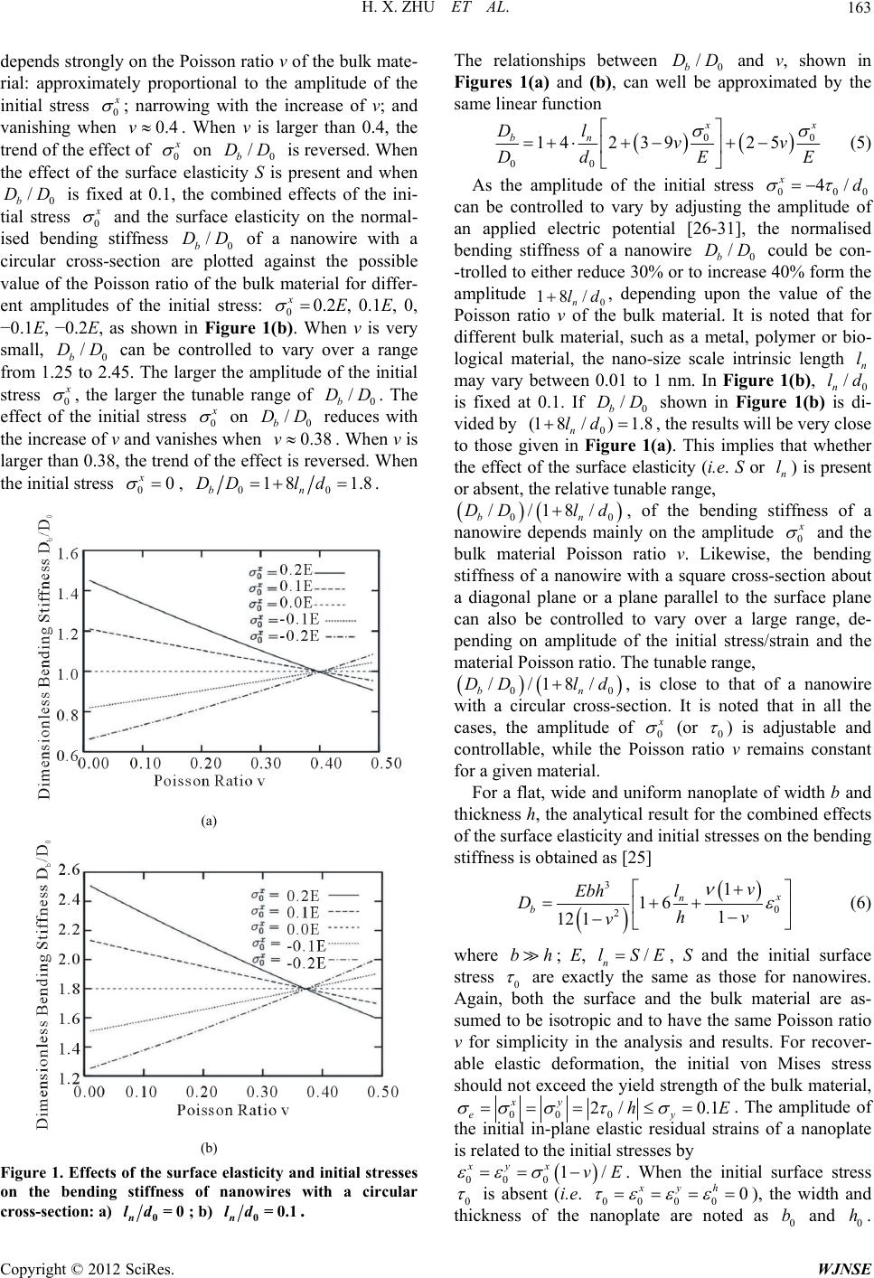 H. X. ZHU ET AL. 163 depends strongly on the Poisson ratio v of the bulk mate- rial: approximately proportional to the amplitude of the initial stress 0 ; narrowing with the increase of v; and vanishing when . When v is larger than 0.4, the trend of the effect of 0 0.4v on 0b is reversed. When the effect of the surface elasticity S is present and when 0 is fixed at 0.1, the combined effects of the ini- tial stress 0 /DD /D b D and the surface elasticity on the normal- ised bending stiffness 0b of a nanowire with a circular cross-section are plotted against the possible value of the Poisson ratio of the bulk material for differ- ent amplitudes of the initial stress: 00.2E, 0.1E, 0, −0.1E, −0.2E, as shown in Figure 1(b). When v is very small, 0 can be controlled to vary over a range from 1.25 to 2.45. The larger the amplitude of the initial stress 0 /DD x / b DD , the larger the tunable range of 0b. The effect of the initial stress 0 /DD on reduces with the increase of v and vanishes when . When v is larger than 0.38, the trend of the effect is reversed. When the initial stress , 0 /D 0.38 b D v 00 x 00 18 1.8ld bn DD . (a) (b) Figure 1. Effects of the surface elasticity and initial stresses on the bending stiffness of nanowires with a circular cross-section: a) 00 n ld=; b) 00.1 n ld= /DD . The relationships between 0b and v, shown in Figures 1(a) and (b), can well be approximated by the same linear function 00 00 142 3925 x bn Dl vv DdE E 4/ xd /DD /81 dl (5) As the amplitude of the initial stress 000 can be controlled to vary by adjusting the amplitude of an applied electric potential [26-31], the normalised bending stiffness of a nanowire 0b could be con- -trolled to either reduce 30% or to increase 40% form the amplitude 0n , depending upon the value of the Poisson ratio v of the bulk material. It is noted that for different bulk material, such as a metal, polymer or bio- logical material, the nano-size scale intrinsic length may vary between 0.01 to 1 nm. In Figure 1(b), 0n is fixed at 0.1. If shown in Figure 1(b) is di- vided by 0n n l /ld 0 / b DD (1 8/)1.8ld n l , the results will be very close to those given in Figure 1(a). This implies that whether the effect of the surface elasticity (i.e. S or ) is present or absent, the relative tunable range, //18/DD ld 00bn , of the bending stiffness of a nanowire depends mainly on the amplitude 0 and the bulk material Poisson ratio v. Likewise, the bending stiffness of a nanowire with a square cross-section about a diagonal plane or a plane parallel to the surface plane can also be controlled to vary over a large range, de- pending on amplitude of the initial stress/strain and the material Poisson ratio. The tunable range, //18/DD ld 00bn , is close to that of a nanowire with a circular cross-section. It is noted that in all the cases, the amplitude of 0 (or 0 ) is adjustable and controllable, while the Poisson ratio v remains constant for a given material. For a flat, wide and uniform nanoplate of width b and thickness h, the analytical result for the combined effects of the surface elasticity and initial stresses on the bending stiffness is obtained as [25] 3 0 2 1 16 1 12 1 n b v l Ebh Dhv v (6) bh/lSE where ; E, n , S and the initial surface stress 0 are exactly the same as those for nanowires. Again, both the surface and the bulk material are as- sumed to be isotropic and to have the same Poisson ratio v for simplicity in the analysis and results. For recover- able elastic deformation, the initial von Mises stress should not exceed the yield strength of the bulk material, 00 0ey . The amplitude of the initial in-plane elastic residual strains of a nanoplate is related to the initial stresses by 2/ 0.1 xy hE 00 1/ xy xvE 0. When the initial surface stress 0 is absent (i.e. 00 00 0 xyh 0 0 h ), the width and thickness of the nanoplate are noted as b and . Copyright © 2012 SciRes. WJNSE 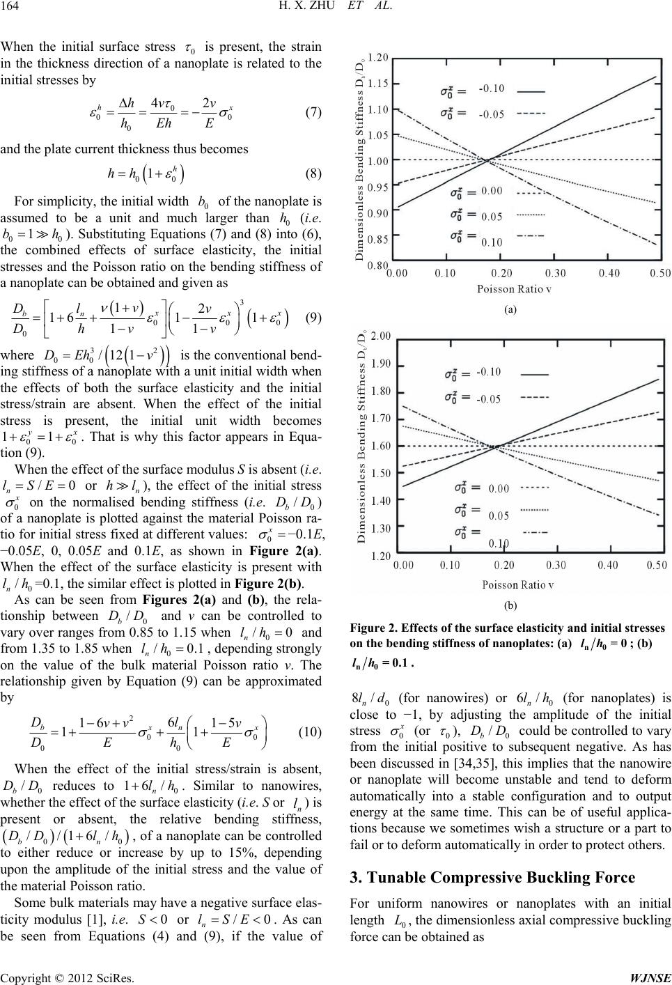 H. X. ZHU ET AL. 164 When the initial surface stress 0 is present, the strain in the thickness direction of a nanoplate is related to the initial stresses by 0 00 2 hx hv h E 0 4v hE 00 1h hh (7) and the plate current thickness thus becomes bh 1bh (8) For simplicity, the initial width 0 of the nanoplate is assumed to be a unit and much larger than 0 (i.e. 00 ). Substituting Equations (7) and (8) into (6), the combined effects of surface elasticity, the initial stresses and the Poisson ratio on the bending stiffness of a nanoplate can be obtained and given as 3 00 2 16 1 1 11 0 0 1 xx bn v Dl v Dhv v 2 1v 3 /12 (9) where 00 is the conventional bend- ing stiffness of a nanoplate with a unit initial width when the effects of both the surface elasticity and the initial stress/strain are absent. When the effect of the initial stress is present, the initial unit width becomes 0 DEh 0 11 yx . That is why this factor appears in Equa- tion (9). When the effect of the surface modulus S is absent (i.e. or n h), the effect of the initial stress 0 /lSE0 nl on the normalised bending stiffness (i.e. 0b) of a nanoplate is plotted against the material Poisson ra- tio for initial stress fixed at different values: 0 /DD x −0.1E, −0.05E, 0, 0.05E and 0.1E, as shown in Figure 2(a). When the effect of the surface elasticity is present with =0.1, the similar effect is plotted in Figure 2(b). 0 As can be seen from Figures 2(a) and (b), the rela- tionship between 0b and v can be controlled to vary over ranges from 0.85 to 1.15 when 0n / n l /D /0lh h D and from 1.35 to 1.85 when 0n/0.1lh , depending strongly on the value of the bulk material Poisson ratio v. The relationship given by Equation (9) can be approximated by 2 00 6 16 1 00 15 1 x n l v hE b D vv DE /D16/lh ) /0lSE 6/lh (10) When the effect of the initial stress/strain is absent, 0b reduces to 0n. Similar to nanowires, whether the effect of the surface elasticity (i.e. S or n lis present or absent, the relative bending stiffness, 0bn , of a nanoplate can be controlled to either reduce or increase by up to 15%, depending upon the amplitude of the initial stress and the value of the material Poisson ratio. D 0 //1DD Some bulk materials may have a negative surface elas- ticity modulus [1], i.e. or n. As can be seen from Equations (4) and (9), if the value of 0S (a) (b) Figure 2. Effects of the surface elasticity and initial stresses on the bending stiffness of nanoplates: (a) n0 =0lh ; (b) n0 =0.1lh 8/ld 6/lh . 0n (for nanowires) or 0n (for nanoplates) is close to −1, by adjusting the amplitude of the initial stress 0 (or 0 ), 0b could be controlled to vary from the initial positive to subsequent negative. As has been discussed in [34,35], this implies that the nanowire or nanoplate will become unstable and tend to deform automatically into a stable configuration and to output energy at the same time. This can be of useful applica- tions because we sometimes wish a structure or a part to fail or to deform automatically in order to protect others. /DD L 3. Tunable Compressive Buckling Force For uniform nanowires or nanoplates with an initial length 0, the dimensionless axial compressive buckling force can be obtained as Copyright © 2012 SciRes. WJNSE 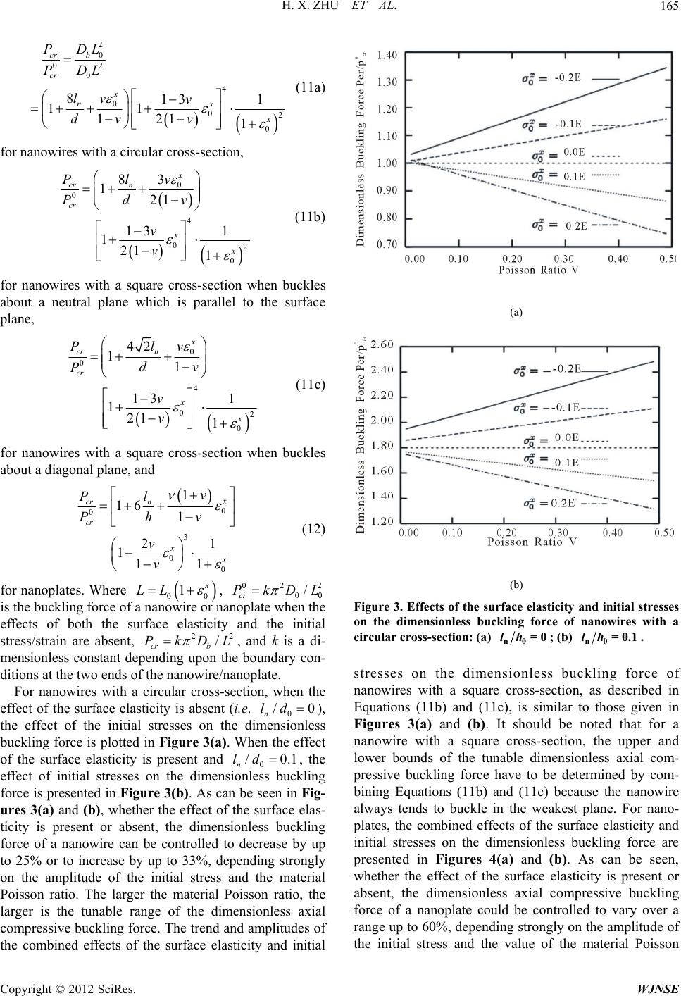 H. X. ZHU ET AL. 165 2 0 02 0 0 0 813 11 121 cr b cr xx n PDL PDL lv v dv v 4 2 0 1 1x (11a) for nanowires with a circular cross-section, 0 4 2 0 1 1 x x v dv 0 0 83 121 13 121 cr n cr x Pl P v v (11b) for nanowires with a square cross-section when buckles about a neutral plane which is parallel to the surface plane, 0 4 2 0 1 1 x x v dv 0 0 42 11 13 121 cr n cr x Pl P v v (11c) for nanowires with a square cross-section when buckles about a diagonal plane, and 0 3 0 0 1 1 21 1 016 11 cr n cr x v hv Pl P v v (12) for nanoplates. Where 00 1 LL 22 / cr b PkDL , 00cr is the buckling force of a nanowire or nanoplate when the effects of both the surface elasticity and the initial stress/strain are absent, , and k is a di- mensionless constant depending upon the boundary con- ditions at the two ends of the nanowire/nanoplate. 022 /PkDL /0ld For nanowires with a circular cross-section, when the effect of the surface elasticity is absent (i.e. 0n (a) (b) Figure 3. Effects of the surface elasticity and initial stresses on the dimensionless buckling force of nanowires with a circular cross-section : (a) ), the effect of the initial stresses on the dimensionless buckling force is plotted in Figure 3(a). When the effect of the surface elasticity is present and 0n/0.1ld , the effect of initial stresses on the dimensionless buckling force is presented in Figure 3(b). As can be seen in Fig- ures 3(a) and (b), whether the effect of the surface elas- ticity is present or absent, the dimensionless buckling force of a nanowire can be controlled to decrease by up to 25% or to increase by up to 33%, depending strongly on the amplitude of the initial stress and the material Poisson ratio. The larger the material Poisson ratio, the larger is the tunable range of the dimensionless axial compressive buckling force. The trend and amplitudes of the combined effects of the surface elasticity and initial n0 =0lh ; (b) n0 =0.1lh . stresses on the dimensionless buckling force of nanowires with a square cross-section, as described in Equations (11b) and (11c), is similar to those given in Figures 3(a) and (b). It should be noted that for a nanowire with a square cross-section, the upper and lower bounds of the tunable dimensionless axial com- pressive buckling force have to be determined by com- bining Equations (11b) and (11c) because the nanowire always tends to buckle in the weakest plane. For nano- plates, the combined effects of the surface elasticity and initial stresses on the dimensionless buckling force are presented in Figures 4(a) and (b). As can be seen, whether the effect of the surface elasticity is present or absent, the dimensionless axial compressive buckling force of a nanoplate could be controlled to vary over a range up to 60%, depending strongly on the amplitude of the initial stress and the value of the material Poisson Copyright © 2012 SciRes. WJNSE  H. X. ZHU ET AL. 166 (a) (b) Figure 4. Effects of the surface elasticity and initial stresses on the dimensionless buckling force of nanoplates: (a) n0 =0lh ; (b) n0 =0.1lh . ratio. It should be noted that the results given in Equa- tions (11) and (12) and shown in Figures 3 and 4 apply only when the nanowires/nanoplates are relatively thin and long (e.g. or /Lh /5/ Ld E ). Otherwise, the nanowire/nanoplate may yield before losing stability. Wang and Feng [21] have studied the combined ef- fects of the surface elasticity and initial surface stress on the axial compressive buckling force of nanowires. However, we do not favour their analysis and results. The initial surface stresses are actually internal stresses in a nanowire or nanoplate because the nanowire/nano- plate contains both the bulk and surface materials. If the initial surface stresses are treated as external tractions, their counterparts (i.e. the initial residual stresses in the bulk material) should also be taken into consideration. Wang and Feng [21] only treated the initial surface stresses as external tractions and ignored the effects of their counterpart, and thus obtained the axial compres- sive buckling force of nanowires as 2 0 22 cr EI Pk d l 2 lEI 22 /2 (13) For a very thin and long nanowire (i.e. ), Equation (13) reduces to 0cr kEIlHHd (see the Equation (11) of paper [21]), suggesting that when the initial surface stress 0 is positive, a very thin and long nanowire will not buckle if the axial compres- sive force is no larger than 0 2d . On the other hand, when the initial surface stress 0 is negative, the bulk material of a nanowire is actually stretched in the longi- tudinal direction by 0 . Equation (13), however, sug- gests that a free thin and long cantilever nanowire, which has already stretched in the longitudinal direction by 0 , would buckle even if a tensile force no larger than 0 2d is axially applied to stretch it at its two ends. The implications of their results (i.e. (13)) are entirely against the common sense. It is noted that the same treatment (i.e. taking the initial surface stresses as external tractions and ignoring the effects of the initial residual stresses in the bulk materials) has appeared in many research papers on studying the bending stiffness, buckling force and reso- nant frequency of nanowires, e.g. [6,11,13,21]. We do not agree with the way of their treatment on the initial surface stress and thus suspect their obtained results. 4. Tunable Natural Frequency For a uniform cantilever nanowire or nanoplate, when the effect of the initial stresses is absent (i.e. 0 or 0 is 0), the natural frequency is given by 44 22 nini i ii ii EI kkD fmL mL n k 3.52k (14) where, is a constant for a given vibration mode, e.g. n for mode 1; 00in for nanowires with a circular cross-section, or 4/6418/DEd ld 4/1218/DEd ld 00in for nanowires with a square cross-section when bending is around a neutral plane parallel to a surface plane, or 41214 2DEd ld 00in for nanowires with a square cross-section when bending is around a diagonal plane, or 3/121 6/ 00in Ehl h mL for nanoplates of an initial unit width; i is the mass of per unit length of the nanowire or nanoplate; and i is the length of the cantilever when the initial stress is absent. When the effect of the initial stresses/strains is present, the normalised natural frequency becomes 3 22 0 1 1 bi ibx ii i Dm LD f fDmL D b D (15) where is the bending stiffness given by Equation (4) Copyright © 2012 SciRes. WJNSE  H. X. ZHU ET AL. 167 for nanowires with a circular cross-section or by Equa- tion (9) for nanoplates; 0 1 i LL // i LL /0.1ld is the length of the nanowire or nanoplate axially stretched by the initial surface stresses, and i because of the mass conservation. mm The effects of the surface elasticity and initial stresses on the normalised natural frequency of a cantilever nanowire with a circular cross-section and 0n and a cantilever nanoplate with 0 are plotted against the Poisson ratio of the bulk material, as shown in Figures 5(a) and (b). We also found that the effect of the amplitude 0 on the relationship given by Equation (15) is so small that it can be neglected. As can be seen in Figures 5( a) and (b), by adjusting the amplitude of the initial stresses (this can be realised by adjusting the am- plitude of an applied electric potential), the normalised natural frequency could be controlled either to reduce or to increase by up to around 20% for nanowires or around 15% for nanoplates from 1, and the tunable range depends upon the amplitude of the initial / n lh0.1 / n ld /i ff (a) (b) Figure 5. Effects of the surface elasticity and initials tresses on the normalised natural frequency: (a) For nanowires with a circular cross-section and n0 =0lh ; (b) For nano- plates with n0 =0.1lh . stresses and the value of the bulk material Poisson ratio. Experiments have demonstrated that micro-or nano-can- tilever wires or plates can be used as sensors to monitor the changes in the natural frequency [17,36], and that the elastic properties, such as the Young’s modulus, of nanowires can be extracted from the measured natural frequency [37]. Lagowski et al. [16] experimentally found that the normal mode of vibration of thin crystals depends strongly on the surface stress. Wang and Feng [11] and He and Lilley [13] have also studied the reso- nant frequency of nanowires. As aforementioned, their results are suspicious because they simply treated the initial surface stresses as external tractions and totally ignored the effects of the initial residual stresses in the bulk material. 5. Conclusion The analytic results obtained in this paper demonstrate that the bending stiffness, resonant frequency, and axial compressive buckling force of a nanowire or nanoplate can be designed either very sensitive or not sensitive at all to the amplitude of the initial stresses (0 or 0 ); show how much those properties can be controlled to vary by adjusting the amplitude of an applied electric potential; and thus provide a reliable guide to the meas- urement of the Young’s modulus of nanowires or nano- plates and to the design of nano-devices, such as nano-sensor or the cantilever of an AFM. 6. Acknowledgements This work is supported by the EC project: PIR-SES- GA-2009-247644. REFERENCES [1] R. E. Miller and V. B. Shenoy, “Size-Dependent Elastic Properties of Nanosized Structural Elements,” Nanotech- nology, Vol. 11, No. 3, 2000, pp. 139-147. doi:10.1088/0957-4484/11/3/301 [2] S. Guenot, C. Fretigny, S. Demoustier-Champagne and B. Nysten, “Surface Tension Effect on the Mechanical Prop- erties of Nanomaterials Measured by Atomic Force Mi- croscopy,” Physical Review B, Vol. 69, No. 16, 2004, pp. 165410.1-165410.5. doi:10.1103/PhysRevB.69.165410 [3] J. H. Song, X. D. Wang, E. Riedo and Z. L. Wang, “Elas- tic Property of Vertically Aligned Nanowires,” Nano Let- ters, Vol. 5, No. 10, 2005, pp. 1954-1958. doi:10.1021/nl051334v [4] G. Y. Jing, H. L. Duan, X. M. Sun, Z. S. Zhang, J. Xu, Y. D. Li, J. X. Wang and D. B. Yu, “Surface Effects on Elastic Properties of Silver Nanowires: Contact Atomic- Force Microscopy,” Physical Review B, Vol. 73, No. 23, 2006, Article ID: 235409. doi:10.1103/PhysRevB.73.235409 Copyright © 2012 SciRes. WJNSE  H. X. ZHU ET AL. 168 [5] C. Q. Chen, Y. Shi, Y. S. Zhang and J. Zhu, Y. J. Yan, “Size Dependent Young’s Modulus in ZnO Nanowires,” Physical Review Letters, Vol. 96, No. 7, 2006, Article ID: 075505. doi:10.1103/PhysRevLett.96.075505 [6] J. He and C. M. Lilley, “Surface Effect on the Elastic Behaviour of Static Bending Nanowires,” Nano Letters, Vol. 8, No. 7, 2008, pp. 1798-1802. doi:10.1021/nl0733233 [7] A. Heidelberg, L. T. Ngo, B. Wu, M. A. Phillips, S. Sharma, T. I. Kamins, J. E. Sader and J. J. Boland, “A Generalized Description of the Elastic Properties of Nanowires,” Nano Letters, Vol. 6, No. 6, 2006, pp. 1101- 1106. doi:10.1021/nl060028u [8] B. Wu, A. Heidelberg and J. J. Boland, “Mechanical Properties of Ultrahigh-Strength Gold Nanowires,” Na- ture Materials, Vol. 4, No. 7, 2005, pp. 525-529. doi:10.1038/nmat1403 [9] X. Li, T. Ono, Y. Wang and M. Esashi, “Ultrathin Sin- gle-Crystalline-Silicon Cantilever Resonators: Fabrication Technology and Significant Specimen Size Effect on Young’s Modulus,” Applied Physics Letters, Vol. 83, No. 15, 2003, pp. 3081-3083. doi:10.1063/1.1618369 [10] H. S. Park, “Surface Stress Effects on the Resonant Prop- erties of Silicon Nanowires,” Journal of Applied Physics, Vol. 103, No. 12, 2008, Article ID: 123504. doi:10.1063/1.2939576 [11] G. F. Wang and X. Q. Feng, “Effects of Surface Elasticity and Residual Surface Stress on the Natural Frequency of Microbeams,” Applied Physics Letters, Vol. 90, No. 23, 2007, Article ID: 231904. doi:10.1063/1.2746950 [12] D. A. Smith, V. C. Holmberg, D. C. Lee and B. A. Korgel, “Young’s Modulus and Size-Dependent Mechanical Quality Factor of Nanoelectromechanical Germanium Nanowire Resonators,” Journal of Physical Chemistry C, Vol. 112, No. 29, 2008, pp. 10725-10729. doi:10.1021/jp8010487 [13] J. He and C. M. Lilley, “Surface Stress Effect on Bending Resonance of Nanowires with Different Boundary Condi- tions,” Applied Physics Letters, Vol. 93, No. 26, 2008, Article ID: 263108. doi:10.1063/1.3050108 [14] H. S. Park, “Quantifying the Size-Dependent Effect of the Residual Surface Stress on the Resonant Frequencies of Silicon Nanowires if Finite Deformation Kinematics Are Considered,” Nanotechnology, Vol. 20, No. 11, 2009, Ar- ticle ID: 115701. doi:10.1088/0957 [15] M. E. Gurtin and X. Markenscoff, “Effect of Surface Stress on the Natural Frequency of Thin Crystals,” Ap- plied Physics Letters, Vol. 29, No. 9, 1976, pp. 529-530. doi:10.1063/1.89173 [16] J. Lagowski, H. C. Gatos and E. S. Sproles Jr, “Surface Stress and the Normal Mode of Vibration of Thin Crys- tals: GaAs,” Applied Physics Letters, Vol. 26, No. 9, 1975, pp. 493-495. doi:10.1063/1.88231 [17] G. Y. Chen, T. Thundat, E. A. Wachter and R. J. War- mack, “Dsorption-Induced Surface Stress and Its Effects on Resonance Frequencey of Microcantilevers,” Journal of Applied Physics, Vol. 77, No. 8, 1995, pp. 3618-3622. doi:10.1063/1.359562 [18] V. V. Dobrokhotov, M. M. Yazdanpanah, S. Pabba, A. Safir and R. W. Cohn, “Visual Force Sensing with Flexi- ble Nanowires Buckling Springs,” Nanotechnology, Vol. 19, No. 3, 2008, Article ID: 035502. doi:10.1088/0957-4484/19/03/035502 [19] C. Hsin, W. Wai, Y. Gu, Y. Gao, C. T. Huang, Y. Liu, L. J. Chen and Z. L. Wang, “Elastic Properties and Buckling of Silicon Nanowires,” Advanced Materials, Vol. 20, No. 20, 2008, pp. 3919-3923. doi:10.1002/adma.200800485 [20] M. Riaz, O. Nur, M. Willander and P. Klason, “Buckling of ZnO Nanowires under Uniaxial Compression,” Applied Physics Letters, Vol. 92, No. 10, 2008, Article ID: 103118. doi:10.1063/1.2894184 [21] G. F. Wang and X. Q. Feng, “Surface Effects on Buckling of Nanowires under Uniaxial Compression,” Applied Physics Letters, Vol. 94, No. 14, 2009, Article ID: 141913. doi:10.1063/1.3117505 [22] F. Xu, Q. Qin, A. Mishra, Y. Gu and Y. Zhu, “Mechani- cal Properties of ZnO Nanowires under Different Loading Modes,” Nano Research, Vol. 3, No. 4, 2010, pp. 271- 280. doi:10.1007/s12274-010-1030-4 [23] K. L. Ekinci, M. H. Huang and M. L. Roukes, “Ultrasen- sitive Nanoelectromechanical Mass Detection,” Applied Physics Letters, Vol. 84, No. 22, 2004, pp. 4469-4471. doi:10.1063/1.1755417 [24] H. X. Zhu, “The Effects of Surface and Initial Stresses on the Bending Stiffness of Nanowires,” Nanotechnology, Vol. 19, No. 40, 2008, Article ID: 405703. doi:10.1088/0957-4484/19/40/405703 [25] H. X. Zhu, J. Wang and B. L. Karihaloo, “Effects of Sur- face and Initial Stresses on the Bending Stiffness of Tri- layer Plates and Nanofilms,” Journal of Mechanics of Materials and Structures, Vol. 4, No. 3, 2009, pp. 589- 604. doi:10.2140/jomms.2009.4.589 [26] J. Biener, A. Wittstock, L. A. Zepeda-Ruiz, M. M. Biener, V. Zielasek, D. Kramer, R. N. Viswanath, J. Wessmuller, M. Baumer and A. V. Hamza, “Surface-Chemistry-Driven Actuation in Nanoporous Gold,” Nature Materials, Vol. 8, No. 1, 2009, pp. 47-51. doi:10.1038/nmat2335 [27] R. Raiteri and H. J. Butt, “Measuring Electrochemically Induced Surface Stress with an Atomic Force Micro- scope,” Journal of Physical Chemistry, Vol. 99, No. 43, 1995, pp. 15728-15732. doi:10.1021/j100043a008 [28] R. C. Cammarata and K. Sieradzki, “Surface and Inter- face Stresses,” Annual Review of Materials Research, Vol. 24, 1994, pp. 215-234. doi:10.1146/annurev.ms.24.080194.001243 [29] J. Weissmuller, R. N. Viswanath, D. Kramer, P. Zimmer, R. Wurschum and H. Gleiter, “Charge-Induced Reversi- ble Strain in a Metal,” Science, Vol. 300, No. 5617, 2003, pp. 312-315. doi:10.1126/science.1081024 [30] D. Kramer, R. N. Viswanath and J. Weissmuller, “Sur- face-Stress Induced Macroscopic Bending of Nanoporous Gold Cantilevers,” Nano Letters, Vol. 4, No. 5, 2004, pp. 793-796. doi:10.1021/nl049927d [31] W. Haiss, R. J. Nichols, J. K. Sass and K. P. Charle, “Linear Correlation between Surface Stress and Surface Charge in Anion Adsorption on Au(111),” Journal of Electroanalytical Chemistry, Vol. 452, No. 2, 1998, pp. Copyright © 2012 SciRes. WJNSE  H. X. ZHU ET AL. Copyright © 2012 SciRes. WJNSE 169 199-202. doi:10.1016/S0022-0728(98)00137-5 [32] J. Diao, K. Gall, M. L. Duan and J. A. Zimmerman, “Atomistic Simulations of the Yielding of Gold Nano- wires,” Acta Materialia, Vol. 54, No. 3, 2006, pp. 643-653. doi:10.1016/j.actamat.2005.10.008 [33] Z. C. Lin and J. C. Huang, “A Study on a Rigid Body Boundary Layer Interface Force Model for Stress Calcu- lation and Stress—Strain Behaviour of Nanoscale Uniax- ial Tension,” Nanotechnology, Vol. 15, No. 11, 2004, pp. 1509-1518. doi:10.1088/0957-4484/15/11/024 [34] H. X. Zhu, “Size-Dependent Elastic Properties of Micro- and Nano-Honeycombs,” Journal of the Mechanics and Physics of Solids, Vol. 58, No. 5, 2010, pp. 696-709. doi:10.1016/j.jmps.2010.02.009 [35] H. X. Zhu, L. B. Yan, R. Zhang and X. M. Qiu, “Size-Dependent and Tunable Elastic Properties of Hier- archical Honeycombs with Regular Square and Equilat- eral Triangular Cells,” Acta Materialia, Vol. 60, No. 12, 2012, pp. 4927-4939. doi:10.1016/j.actamat.2012.05.009 [36] V. Tabard-Cossa, M. Godin, L. Y. Beaulieu and P. Grut- ter, “A Differential Microcantilever-Based System for Measuring Surface Stress Changes Inducted by Electro- chemical Rection,” Sensors and Actuators B: Chemical, Vol. 107, No. 1, 2005, pp. 233-241. doi:10.1016/j.snb.2004.10.007 [37] Z. L. Wang, Z. R. Dai, R. P. Gao and J. L. Gole, “Meas- uring the Young’s Modulus of Solid Nanowires by in Situ TEM,” Journal of Electron Microscopy, Vol. 51, Suppl. 1, 2002, pp. S79-S85. doi:10.1093/jmicro/51.Supplement.S79
|