Journal of Modern Physics
Vol.3 No.9(2012), Article ID:22619,4 pages DOI:10.4236/jmp.2012.39138
Effect of the Heat Treatments on the Dopes Segregation in Polycrystalline Silicon Films
Laboratory of Semiconductors, Department of Physics, University Badji Mokhtar, Annaba, Algeria
Email: silinis2@yahoo.fr
Received July 2, 2012; revised August 3, 2012; accepted August 10, 2012
Keywords: Segregation; Grains Boundaries; Heat Treatments; Polycrystalline Silicon
ABSTRACT
In this work we are interested in studying the effect of the heat treatments on the dopant segregation at the grain boundaries in the polycrystalline silicon films. The obtained results have shown that the heat treatments reduce the number of segregation sites at the grains boundaries, and consequently they limit the structural changes that can appear there and the quantity of the dope atoms that can accumulate in these boundaries. In addition there are more and more dopant that are found inside the grains when the temperature of the heat treatment increases. On the other hand, we established that the arsenic atoms have a strong tendency to the segregation than the boron atoms, and we have noticed a strong migration of arsenic atoms from the boundaries towards the grains under the effect of the heat treatments. It was also shown that the segregation of arsenic atoms at the grains boundaries is about 4 times higher than that of the boron atoms.
1. Introduction
The circuit complexity and the more and more high degree of component integration require continuous improvement and the mastery of the properties of the polycrystalline silicon [1-7].
In many of its applications, this material is subjected to various heat treatments in order to increase the grains size, to reduce the defects and allow the implanted ions to occupy positions where they are electrically active. In the frame work of this study we are interested in the effect of the heat treatments on the dopant segregation at the grain boundaries of the polycrystalline silicon films that are boron and/or arsenic doped and subjected to different heat treatments.
2. Experimental Conditions
In order to study the influence of the heat treatments on the dopant segregation in the polycrystalline silicon, measurements of Hall effect and resistivity were carried out on Si-poly films whose thickness is 7×10⁻⁵ cm. These films were doped with boron and/or arsenic (1015 cm−2) by ionic implantation (180 kev). Heat treatments were carried out before implantation at the temperatures of 1000˚C to 1150˚C during 120 mn. An annealing after implantation at 1100˚C for 30 mn permits the rearrangement of the network atoms and the redistribution of the dopant.
If we admit, on the one hand that the annealing after implantation that we have carried out allow the dopant atoms in the grain to take position in the substitution sites, and on the other hand that all these atoms are ionized at 20˚C the concentration of the dopant atoms at the grains boundaries will be equal to the difference between the total concentration and that of the ionized atoms (atoms in the grains)
 (1)
(1)
Moreover the concentration of the ionized atoms is equal to the sum of the concentrations of the free carriers and the trapped carriers
 (2)
(2)
withNt: density of the trapped carriers;
L: grain size.
The apparent concentration of the free carriers was obtained by Hall effect measurements for different heat treatments. Thus we have to determine the concentration of the trapped carriers for these same heat treatments.
For grains partially deserted by carriers and trap states entirely filled, the height of the potential barriers of the deserted regions is given by [8]:
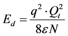 (3)
(3)
withQt: density of the trap states at the grain boundaries;
ε: dielectric constant of the polycrystalline silicon.
By replacing  by
by  and N by
  in Equation (3), one obtains the expression of the density of the trapped carriers:
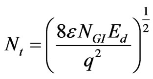 (4)
(4)
If we substitute Equation (4) in Equation (2), we obtain a quadratic equation in  whose resolution gives the expression of ionized atoms concentration:
 (5)
(5)
By comparing (2) and (5), we deduce the expression of the concentration of the trapped carriers:
 (6)
(6)
The concentration of the trapped carriers for different heat treatments is obtained after the determination of the potential barrier height of the deserted regions Ed from the characteristics  [9] by using the resistivity equation given by Mandurah et al. [10].
The Figures 1 and 2 show the reduction of the dopant concentration in the boundaries when the temperature of the heat treatments before implantation increases. Indeed the heat treatments reduce the number of segregation sites at the grains boundaries, and consequently, they limit the quantity of the dopant that may accumulate in these boundaries. We have noticed that there are more and more dopant that are found inside the grains when the temperature of the heat treatments increases. On the other hand we established that the arsenic atoms have a strong segregation tendency at the grains boundaries than the boron atoms (about 4 times higher), and we have noticed a strong migration of arsenic atoms from the boundaries toward the grains under the effect of the heat treatments.
For the boron doping the dopants concentration in the grains is always greater than the dopants concentrations that are found at the grains boundaries, regardless of the heat treatments temperature. In the case of the arsenic doping we notice that there are many more arsenic atoms at the boundaries than those inside the grains for the heat treatments temperature lower than 1100˚C.
The increase of the free carriers concentration with the temperature of the heat treatments before implantation is due to tow effects; the reduction of the trap states and the
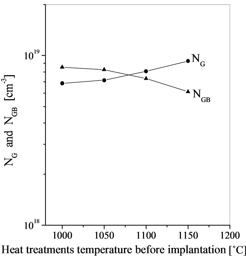
Figure 1. Concentration of the arsenic atoms in the grains and at the grain boundaries vs. the heat treatments temperature before implantation.
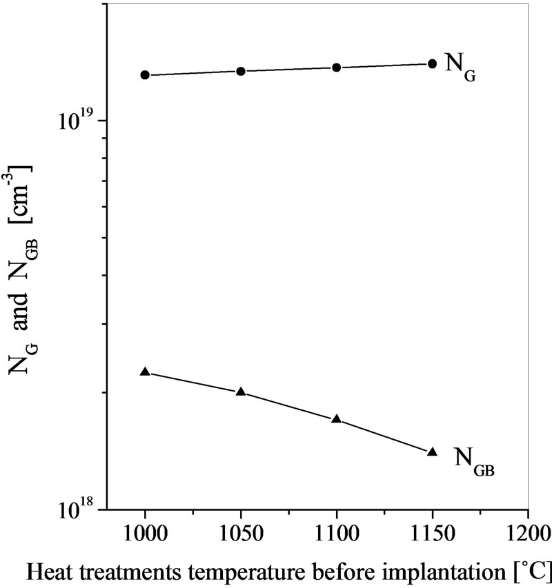
Figure 2. Concentration of the boron atoms in the grains and at the grain boundaries vs. the heat treatments temperature before implantation.
segregation sites, leading to the freeing of some carriers and the diminution of the quantity of dopant at the grains boundaries. However the increase of the dopant concentration in the grains with these same temperatures can be attributed only to the reduction of dopant quantity at the boundaries.
From Figures 3 and 4, we notice that the ratio NGB/N relative to the dopant average concentration diminishes when the heat treatments temperature increases. This diminution is more pronounced for the arsenic doping. In these two figures, it is also shown that the increase of the dopant proportion in the grains is low for the
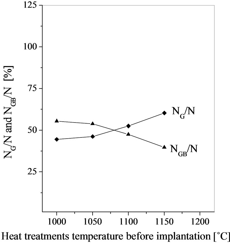
Figure 3. Ratio of concentration NG/N and NGB/N of the arsenic atoms vs. heat treatments temperature before implantation.
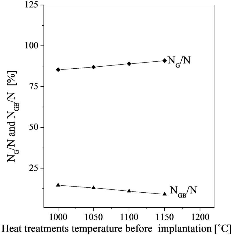
Figure 4. Ratio of concentration NG/N and NGB/N of the boron atoms vs. heat treatments temperature before implantation.
temperatures below 1050˚C, and then becomes more pronounced for the too higher temperatures. The low variation, in the range 1000˚C - 1050˚C is explained by the heat treatment effect after implantation (1100˚C; 30 mn), which increases the size of the grains, reduces the volume of the boundaries and displaces the dopant from the boundaries towards the grains.
On the other hand, the heat treatment effect on the films that were treated before implantation at T > 1050˚C is negligible.
Mei and Dutton [11] have shown that the dopant segregation at the grains boundaries diminishes, in one hand with the thickness of the polycrystalline silicon film, and on the other hand with the increase of the grains size.
Indeed, the growth of the grains, when the thickness of the film increases or under the effect of a heat treatment at high temperature [12], reduces the total volume of the boundaries, and consequently the density of the segregation sites.
5. Conclusion
This study has shown that the heat treatments reduce the number of segregation sites at the grains boundaries, and consequently, they limit the structural changes that can appear there and the quantity of dope atoms that can accumulate in these boundaries. In addition, there are more and more dopant that are found inside the grains when the temperature of the heat treatments increases. On the other hand, we established that the arsenic atoms have a strong segregation tendency at the grains boundaries than the boron atoms (about four times higher), and we have noticed a strong migration of arsenic atoms from the boundaries towards the grains under the effect of the heat treatments.
REFERENCES
- B. Hadjoudja and A. Chibani, “Global Model for Electrical Conduction in Polysilicon Layers,” Annales de Chimie—Science des Matériaux, Vol. 31, No. 1, 2006, pp. 121-134. doi:10.3166/acsm.31.121-134
- S. Honda, T. Mates, M. Ledinsky, J. Oswald, A. Fejfar, J. Koeka, T. Yamazaki, Y. Uraoka and T. Fuyuki, “Effect of Hydrogen Passivation on Polycrystalline Silicon Thin Films,” Thin Solid Films, Vol. 487, No. 1-2, 2005, pp. 152-156. doi:10.1016/j.tsf.2005.01.056
- A. Haddad, T. Inokuma, Y. Kurata and S. Hasegawa, “Characterization of Structure and Role of Different Textures in Polycrystalline Si Films,” Journal of Non-Crystalline Solids, Vol. 351, No. 24-26, 2005, pp. 2107-2114. doi:10.1016/j.jnoncrysol.2005.05.007
- D. D. Malinovska, O. Angelov, M. S. Vassileva, M. Kamenova and J. C. Pivin, “Polycrystalline Silicon Thin Films on Glass Substrate,” Thin Solid Films, Vol. 451- 452, 2004, pp. 303-307. doi:10.1016/j.tsf.2003.11.054
- A. Slaoui, E. Pihan, I. Ka, N. A. Mbow, S. Roques and J. M. Koebel, “Passivation and Etching of Fine-Grained Polycrystalline Silicon Films by Hydrogen Treatment,” Solar Energy Materials & Solar Cells, Vol. 90, No. 14, 2006, pp. 2087-2098. doi:10.1016/j.solmat.2006.02.004
- B. Ai, H. Shen, Z. Liang, Z. Chen, G. Kong and X. Liao, “Electrical Properties of B-Doped Polycrystalline Silicon Thin Films Prepared by Rapid Thermal Chemical Vapour Deposition,” Thin Solid Films, Vol. 497, No. 1-2, 2006, pp. 157-162. doi:10.1016/j.tsf.2005.10.069
- R. Mahamdi, F. Mansour, E. Scheid, B. T. Boyer and L. Jalabert, “Boron Diffusion and Activation during Heat Treatment in Heavily Doped Polysilicon Thin Films for P+ Metal-Oxide-Semiconductor Transistors Gates,” Japanese Journal of Applied Physics, Vol. 40, 2001, pp. 6723- 6727. doi:10.1143/JJAP.40.6723
- J. Y. W. Seto, “The electrical properties of polycrystalline silicon films,” Journal of Applied Physics, Vol. 46, No. 12, 1975, pp. 5247-5254. doi:10.1063/1.321593
- B. Hadjoudja, A. Chibani, R. Zeggari and B. Chouial, “Modélisation des Variations de la Résistivité des Couches de Silicium Polycristallin,” Physical & Chemical News, Vol. 13, 2003, pp. 85-90.
- M. M. Mandurah, K. C. Saraswat and T. I. Kamins, “A Model for Conduction in Polycrystalline Silicon—Part I: Theory,” IEEE Transactions on Electron Devices, Vol. 28, No. 10, 1981, pp. 1163-1171. doi:10.1109/T-ED.1981.20504
- L. Mei and R. W. Dutton, “A Process Simulation Model for Multilayer Structures Involving Polycrystalline Silicon,” IEEE Transactions on Electron Devices, Vol. 29, No. 11, 1982, pp. 1726-1734. doi:10.1109/T-ED.1982.21017
- J. Murota and T. Sawai “Electrical Characteristics of Heavily Arsenic and Phosphorus Doped Polycrystalline Silicon,” Journal of Applied Physics, Vol. 53, No. 5, 1982, pp. 3702-3708. doi:10.1063/1.331157

