Preparation of Thin Films by a Bipolar Pulsed-DC Magnetron Sputtering System Using Ca3Co4O9 and CaMnO3 Targets
646
on
t
off
t
Time
Cathode
Anode
100 High Voltage Probe
Oscilloscope
Bipolar
Pulsed-DC
Power
Supply
+V
V
+
off
t
on
t
Vacuum
Chamber
Magnetron
Sputtering
Gun, Target
Argon (Ar)
Substrate
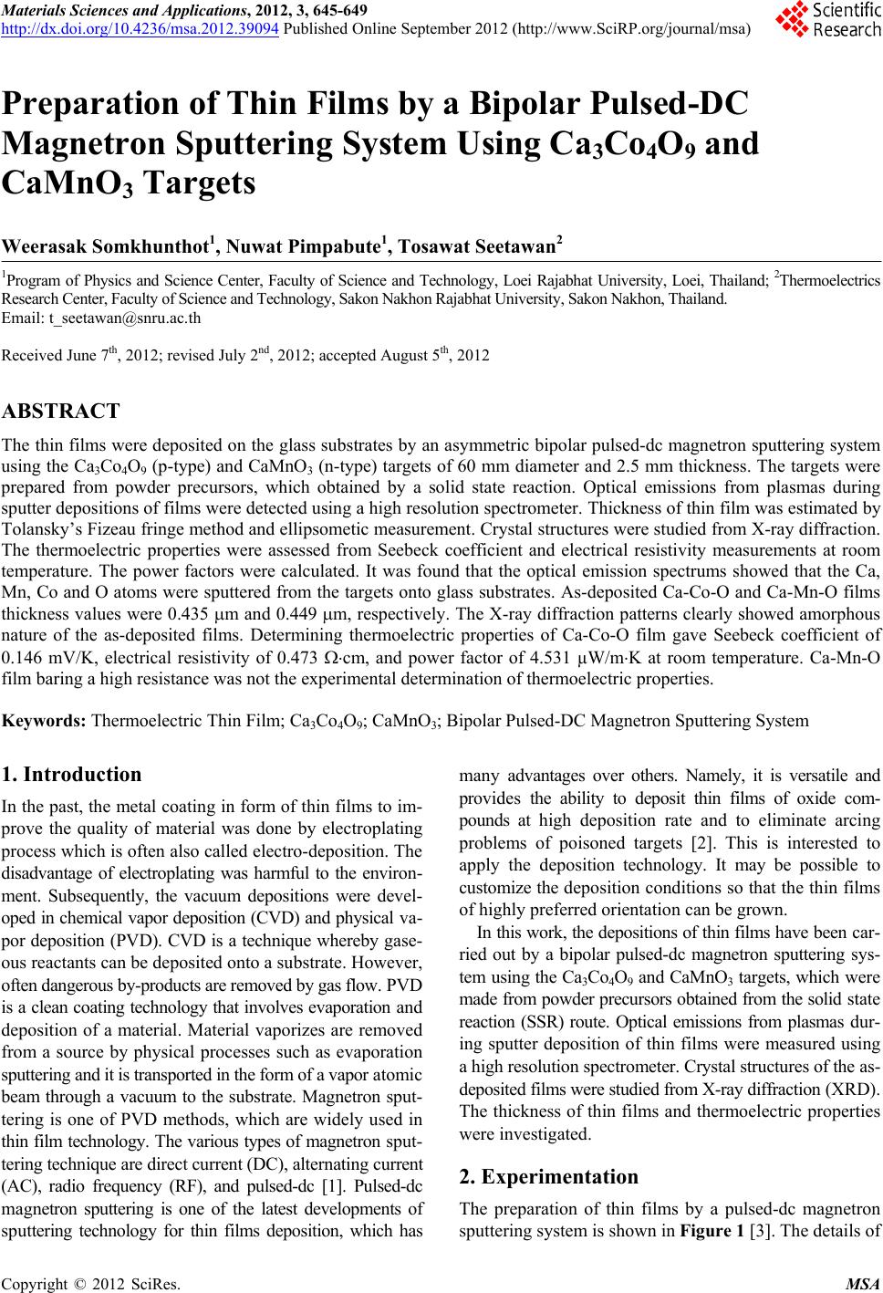
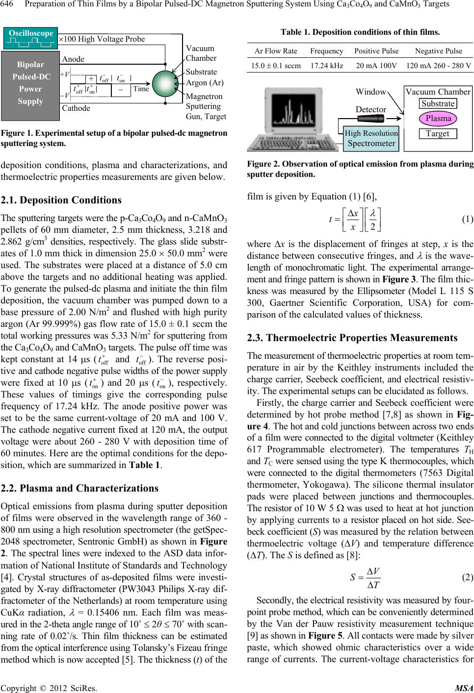
Figure 1. Experimental setup of a bipolar pulsed-dc magnetron
sputtering system.
deposition conditions, plasma and characterizations, and
thermoelectric properties measurements are given below.
2.1. Deposition Conditions
The sputtering targets were the p-Ca3Co4O9 and n-CaMnO3
pellets of 60 mm diameter, 2.5 mm thickness, 3.218 and
2.862 g/cm3 densities, respectively. The glass slide substr-
ates of 1.0 mm thick in dimension 25.0 50.0 mm2 were
used. The substrates were placed at a distance of 5.0 cm
above the targets and no additional heating was applied.
To generate the pulsed-dc plasma and initiate the thin film
deposition, the vacuum chamber was pumped down to a
base pressure of 2.00 N/m2 and flushed with high purity
argon (Ar 99.999%) gas flow rate of 15.0 ± 0.1 sccm the
total working pressures was 5.33 N/m2 for sputtering from
the Ca3Co4O9 and CaMnO3 targets. The pulse off time was
kept constant at 14 s (off and off
t). The reverse posi-
tive and cathode negative pulse widths of the power supply
were fixed at 10 s (on ) and 20 s (on
t), respectively.
These values of timings give the corresponding pulse
frequency of 17.24 kHz. The anode positive power was
set to be the same current-voltage of 20 mA and 100 V.
The cathode negative current fixed at 120 mA, the output
voltage were about 260 - 280 V with deposition time of
60 minutes. Here are the optimal conditions for the depo-
sition, which are summarized in Table 1.
t
t
2.2. Plasma and Characterizations
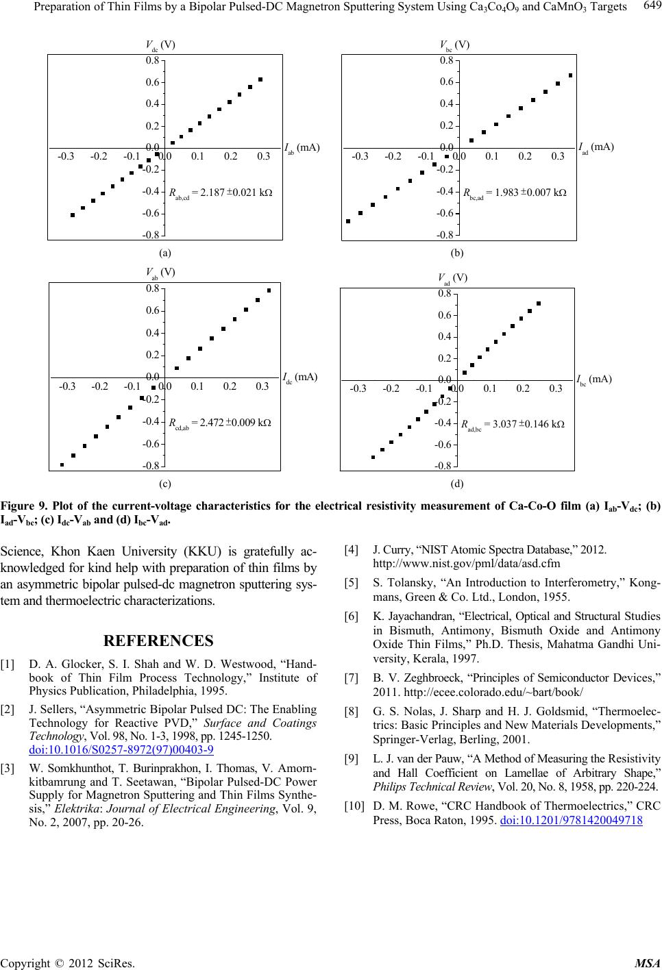
Optical emissions from plasma during sputter deposition
of films were observed in the wavelength range of 360 -
800 nm using a high resolution spectrometer (the getSpec-
2048 spectrometer, Sentronic GmbH) as shown in Figure
2. The spectral lines were indexed to the ASD data infor-
mation of National Institute of Standards and Technology
[4]. Crystal structures of as-deposited films were investi-
gated by X-ray diffractometer (PW3043 Philips X-ray dif-
fractometer of the Netherlands) at room temperature using
CuKα radiation,
= 0.15406 nm. Each film was meas-
ured in the 2-theta angle range of 10˚ 2θ 70˚ with scan-
ning rate of 0.02˚/s. Thin film thickness can be estimated
from the optical interference using Tolansky’s Fizeau fringe
method which is now accepted [5]. The thickness (t) of the
Table 1. Deposition conditions of thin films.
Ar Flow RateFrequency
Positive Pulse Negative Pulse
sccm kHz mA V mA - V
Plasma
High Resolution
Spectrometer
Window
DetectorSubstrat e
Target
Vacuum Chamber
Figure 2. Observation of optical emission from plasma during
sputter deposition.
film is given by Equation (1) [6],
2
x
tx
(1)
where x is the displacement of fringes at step, x is the
distance between consecutive fringes, and
is the wave-
length of monochromatic light. The experimental arrange-
ment and fringe pattern is shown in Fi gure 3 . The film thic-
kness was measured by the Ellipsometer (Model L 115 S
300, Gaertner Scientific Corporation, USA) for com-
parison of the calculated values of thickness.
2.3. Thermoelectric Properties Measurements
The measurement of thermoelectric properties at room tem-
perature in air by the Keithley instruments included the
charge carrier, Seebeck coefficient, and electrical resistiv-
ity. The experimental setups can be elucidated as follows.
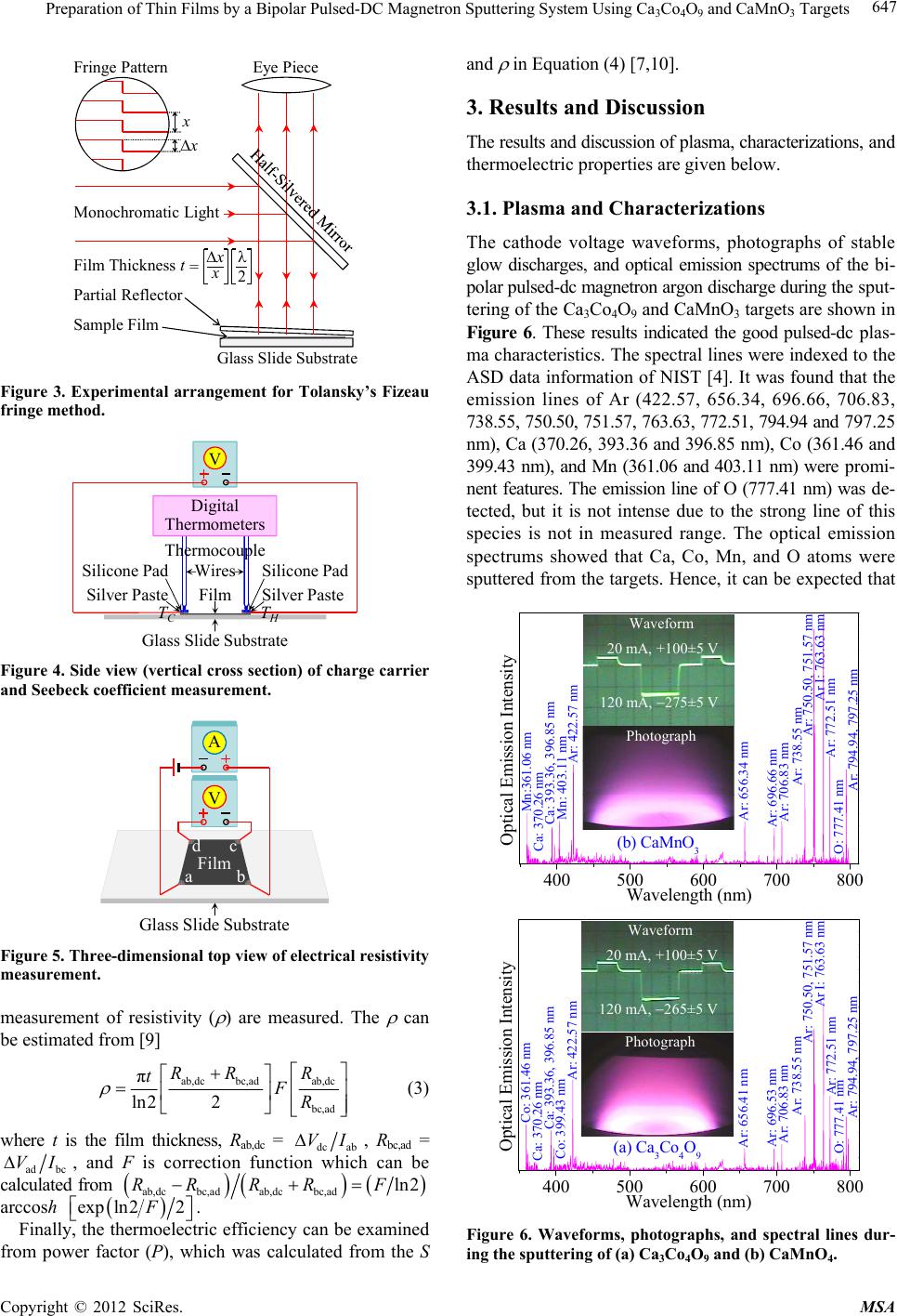
Firstly, the charge carrier and Seebeck coefficient were
determined by hot probe method [7,8] as shown in Fig-
ure 4. The hot and cold junctions between across two ends
of a film were connected to the digital voltmeter (Keithley
617 Programmable electrometer). The temperatures TH
and TC were sensed using the type K thermocouples, which
were connected to the digital thermometers (7563 Digital
thermometer, Yokogawa). The silicone thermal insulator
pads were placed between junctions and thermocouples.
The resistor of 10 W 5 was used to heat at hot junction
by applying currents to a resistor placed on hot side. See-
beck coefficient (S) was measured by the relation between
thermoelectric voltage (V) and temperature difference
(T). The S is defined as [8]:
V
ST
(2)
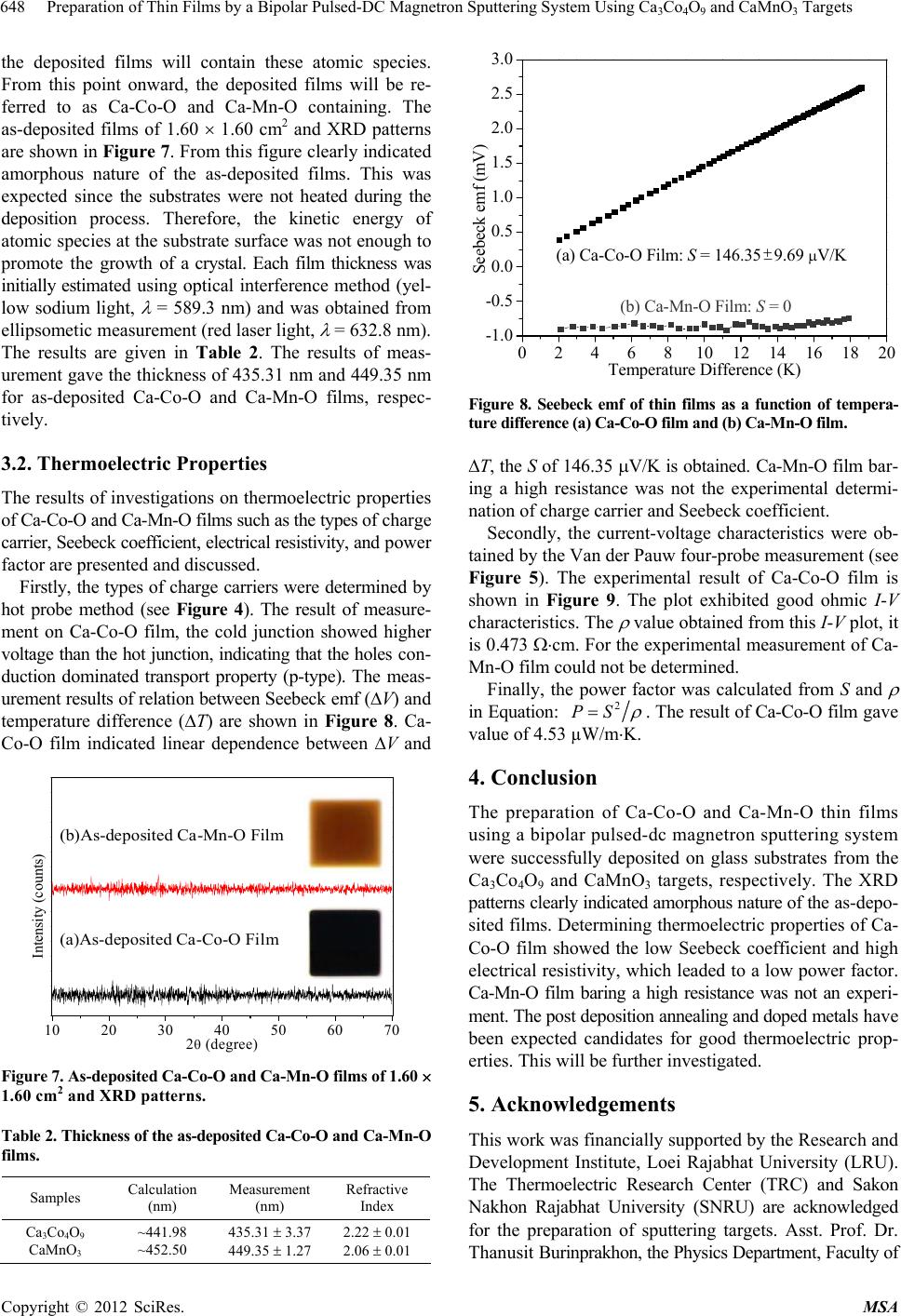
Secondly, the electrical resistivity was measured by four-
point probe method, which can be conveniently determined
by the Van der Pauw resistivity measurement technique
[9] as shown in Figure 5. All contacts were made by silver
paste, which showed ohmic characteristics over a wide
range of currents. The current-voltage characteristics for
Copyright © 2012 SciRes. MSA