Circuits and Systems
Vol.07 No.08(2016), Article ID:67249,12 pages
10.4236/cs.2016.78122
Rapid Prototype with Field Gate (A Design and Implementation of Stepper Motor Using FPGA)
Warsame H. Ali, Emmanuel S. Kolawole, Pamela Obiomon, John H. Fuller, Shukri Ali, Penrose Cofie
Department of Electrical and Computer Engineering, Prairie View A&M University, Prairie View, USA

Copyright © 2016 by authors and Scientific Research Publishing Inc.
This work is licensed under the Creative Commons Attribution International License (CC BY).
http://creativecommons.org/licenses/by/4.0/


Received 10 March 2016; accepted 10 April 2016; published 9 June 2016
ABSTRACT
This paper presents the design and implementation of a Stepper Motor using Nexys2 circuit board based on a Xilinx Spartan 3E Field Programmable Gate Array (FPGA) device with VHDL code. The algorithm implemented on FPGA allows a substantial decrease of the equivalent processing time developed by different velocity controllers. The Stepper Speed control is achieved using VHDL code, and the hardware digital circuit is designed for a programmable rotational stepper motor using VHDL as a tool and FPGA as a target technology. The 50 MHZ provided by the starter kit is divided to obtain the necessary delay time between the motor phases that ranges between 2 - 10 m seconds. Though output selections, the direction of rotation of the stepper motor besides the magnitude of the angle of movement and the rotation speed can be controlled. The major advantage of using reconfigurable hardware (FPGA) in implementing the Stepper Motor instead of a discrete digital component is that it makes modifications to the design easy and quick and also, the total design hence represents an embedded system (works without computer). The total programmable hardware design that controlled on the stepper motor movement, occupied an area that did not exceed 12% of the chip resources.
Keywords:
Stepper Motor, Xilinx Spartan 3E FPGA, Xilinx ISE Tools, User I/O, LEDS, PMOD, Motion Control, VHDL, PLANAHEAD

1. Introduction
A stepper motor is an electrically powered motor that creates rotation from electrical current driven into the motor. Physically, stepper motors can be large but are often small enough to be driven by current on the order of milliampere. Current pulses are applied to the motor, and this generates discrete rotation of the motor shaft [1] . This is unlike a DC motor that exhibits continuous rotation. Although it is possible to drive a stepper motor in a manner where it has near continuous rotation, doing so requires more finesse of the input waveform that drives the stepper motor. It is an electro mechanical device, which converts electrical pulses into discrete mechanical movements. The shaft or spindle of a stepper motor rotates indiscrete step increments when electrical command pulses are applied to it in the proper sequence. The sequence of the applied pulses is directly related to the direction of motor shafts rotation. The speed of the motor shafts rotation is directly related to the frequency of the input pulses and the length of rotation of input pulses applied. One of the most significant advantages of a stepper motor is its ability to be accurately controlled in an open loop system. Open loop control means no feedback information about position is needed. This type of control eliminates the need for expensive sensing and feedback devices such as optical encoders. Your position is known simply by keeping track of the input step pulses.
Stepper motor is used in broad application for speed and position control. In this paper, the speed profile of stepper motor is analyzed based on Field Programmable Gate Implementation (FPGA). As a speed moving motor, it must have rising and falling process which includes missing steps by steps. FPGA gives the different control method for controlling the speed of stepper motor
To avoid missing steps, the system based on FPGA has good interfacing, thus we can interface more than one stepper motors for further application [2] . Figure 1 and Figure 2 show Stepper Motor block diagram and internal connection.
There are three basic stepper motor types. They are:
・ Variable-reluctance
・ Permanent-magnet
・ Hybrid.
2. Stepper Motor Design and Methodology
The stepper motor shown in Figure 3 has four coils (called A, B, C and D), each slightly offset from the other.
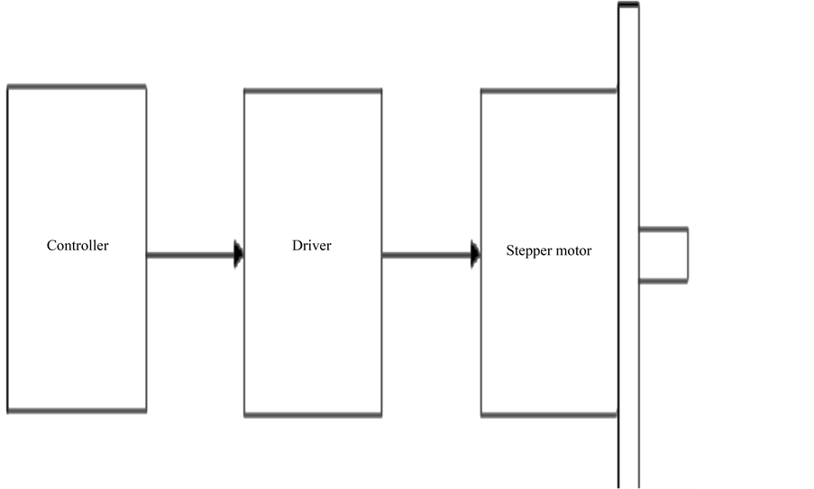
Figure 1. Block diagram of stepper motor control.

Figure 2. Stepper motor internal connection.
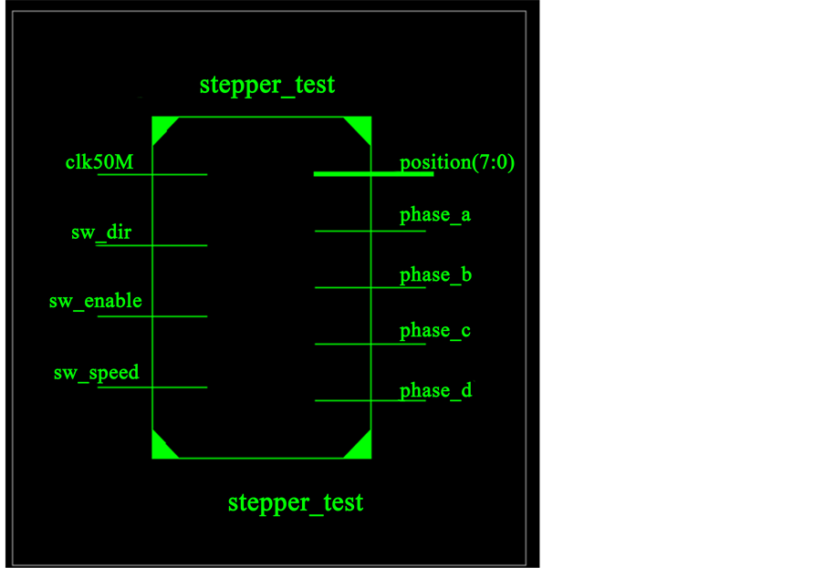
Figure 3. Stepper motor design.
When different phase coils are powered the motor will move a very small amount, and if you change quick enough then smooth rotation can be achieved [3] . This design uses full stepping, where pairs of coils (A + B, B + C, C + D or D + A) are always powered, which is the simplest way to use the motor. The maximum power of the signals from the FPGA is too small to drive the motor directly, a small driver board is used to amplify these control signals and power the coils.
In designing and implementing the Stepper Motor using FPGA, a Nexys2 circuit board based on a Xilinx Spartan 3E Field Programmable Gate Array (FPGA) device with VHDL code is used which is the controller as shown in Figure 4 consisting of FPGA Board, Driver and Stepper Motor [4] .
In this design, the inputs to the FPGA and the Pmod pins location as shown in Figure 5 on the Board are narrated below;
NET "clk50M" LOC = B8
The clk50M pin connects to a 50 MHz clock on the FPGA development board. It is this clock signal that co-ordinates all activities on the FPGA. The period of this signal should be specified, so that the tools can make sure that all of the design’s logic functions correctly at this speed (as the design is limited by the switching speed of the FPGA’s logic and the speed at which signals propagate across the chip). Note the clk50m Pin is connected to B8 on the FPGA [6] .
NET "sw_dir" LOC = "H18";
NET "sw_enable" LOC = "G18";
NET "sw_speed" LOC = "K18";

Figure 4. Stepper motor implementation using FPGA nexys2 circuit board.

Figure 5. PMOD Pin locations on FPGA [5] .
The “sw_” signals are connected to the switches which equally serve as the input to the FPGA.
"sw_dir" LOC = "H18"; this is the input switch that coordinate the direction of the motor either to rotate to the left when the signal is high “1” or to rotate to the left when the signal is low “0”. Note the sw_dir Pin is connected to H18 on the FPGA.
"sw_enable" LOC = "G18"; this is the input switch that enable or powered the motor to start operation when the signal is high “1” or disable or stop the motor operation when the signal is low “0”. Note the sw_enable Pin is connected to G18 on the FPGA.
"sw_speed" LOC = "K18"; this is the input switch that coordinate or adjust the speed of the motor by increasing the speed as specified in the VHDL code/ program when the signal is high “1” or reduce the speed when the signal is low “0”. Note the sw_speed Pin is connected to K18 on the FPGA.
Also, the outputs of the FPGA as designed are narrated below.
NET "phase_a" LOC = "L15";
NET "phase_b" LOC = "K12";
NET "phase_c" LOC = "L17";
NET "phase_d" LOC = "M15";
NET "position<0>" LOC = "J14";
NET "position<1>" LOC = "J15";
NET "position<2>" LOC = "K15";
NET "position<3>" LOC = "K14";
NET "position<4>" LOC = "E17";
NET "position<5>" LOC = "P15";
NET "position<6>" LOC = "F4";
NET "position<7>" LOC = "R4".
On the FPGA board “phase_” signals are connected to the PMOD connector, the “position” signals are connected to the LEDs.
"phase_a" LOC = "L15";
"phase_b" LOC = "K12";
"phase_c" LOC = "L17";
"phase_d" LOC = "M15".
These phase_a thru d are the outputs from the FPGA through the PMOD interface JA and connected to the Stepper Motor through the Motor driver as shown in Figure 4. Note their corresponding locations on the FPGA pins are shown in Figure 5 drafted from the Diligent Nexys2 Board Reference Manual. That is; Phase_a is connected to L15, Phase_b is connected to K12, Phase_c is connected to L17, and Phase_d is connected to M15.
Also, the “position” signals are connected to the LEDs on the Board with their corresponding pin locations.
NET "position<0>" LOC = "J14";
NET "position<1>" LOC = "J15";
NET "position<2>" LOC = "K15";
NET "position<3>" LOC = "K14";
NET "position<4>" LOC = "E17";
NET "position<5>" LOC = "P15";
NET "position<6>" LOC = "F4";
NET "position<7>" LOC = "R4".
The speed for a reactive motor is given by the formula

where f is the pulse frequency;  is the step angle [7] .
The pulse frequency changes due to fluctuations in the environmental conditions. Thus a fixed number of step-by-step operations are done in every week so that the step error will not accumulate and change the pulse frequency. In actual position of stepper motor control, we must inevitably face the issue of speed. To avoid the lost step phenomenon the general requirement for the highest operating frequency should be less than (or equal) stepper motor in response to the frequency. This is the operating frequency in which stepper motor can start, stop or reverse rather than out of step phenomenon.
Figure 6 shows the in/outputs pin connections on the FPGA through the PLANAHEAD.
Figure 6 shows the clock, input and output locations on the FPGA Board as described above. This displays how they are being connected on the board and displayed using the PLANAHEAD tool during synthesis and clocking operation.
3. Stepper Motor Implementation on FPGA Using VHDL Coding
In this paper, the successful implementation of Stepper Motor using FPGA is achieved using Xilinx Spartan 3E Field Programmable Gate Array (FPGA) device and programmed by VHDL code [8] .
Figure 7 shows the VHDL design flow chart during this implementation of Stepper Motor. The flow chart starts with the general compilation of hardware such as FGPA Spartan 3E Board, Pmod driver Board, Stepper Motor, VHDL Code compilation as shown in Figure 8 (this is the actual VHDL Code that was developed to program the FPGA Board following the process of Gate Synthesis and Co-Simulation which then generated the bit that was downloaded to the Board that then powers the Stepper Motor on stand-by; that is without being connected to the computer).
During the implementation, the function of the Pmod driver Board as shown in Figure 4 is to transfer the minimal amount of power needed to turn on the Stepper Motor with the aid of a jumper cable attached between the FPGA Board and the Stepper Motor.
4. Result and Discussion
To analyze the performance of this system, the algorithm was implemented on Xilinx Spartan 3E Field Programmable Gate Array (FPGA) device. A constraints file which defines the input and output signals of the logical design are connected to each pins on the outside of the chip. The chip used is a Ball Grid Array chip, and

Figure 6. Pin locations on PLANAHEAD.

Figure 7. VHDL design flow chart [10] .


Figure 8. VHDL codes for stepper motor on FPGA.
pins are located with a letter for the column and a number for the row. In this design we are using 16 pins, but the FPGA has many more available.
There is one special pin, the clk50M pin, which connects to a 50 MHz clock on the FPGA development board. It is this clock signal that co-ordinates all activities on the FPGA. The period of this signal should be specified, so that the tools can make sure that all of the design’s logic functions correctly at this speed (as the design is limited by the switching speed of the FPGA’s logic and the speed at which signals propagate across the chip). This design has three internal signals, and that also act as registers (they “hold” values). The “coils” is initialized to “0011” as it will be connected to the output of the design that powers the stepper motor, and coils A and B will be initially powered. The sizes of these signals have been carefully chosen = coils has to hold the four outputs for the stepper motor, count has to hold number to 400,000 and step count has to hold the position to be indicated on the eight LEDs.
Figure 9 shows RTL schematic and Figures 10-14 shows simulation results of the VHDL code. The VHDL code was written and simulated in XILINX ISE 14.7i [9] .

Figure 9. RTL schematic.

Figure 10. Stepper motor waveform.

Figure 11. Stepper motor implementation hardware co-simulation using FPGA successful.


Figure 12. Logic schematic.
Figure 9 shows the RTL Schematic output simulation of the implementation on the Stepper Motor on FPGA.
Figure 10 displays the Stepper Motor waveform showing constraints as applied to the FPGA such as, input and output LEDs, the phases on the Motor, Motor driver and the clock time application.
Figure 11 shows the successful Hardware Co-simulation of FPGA thereby generating the bit file that was downloaded to power on the Stepper without being connected to the computer system (Stepper Motor on stand-alone operation).
Figure 12 shows the logic Schematic that displays the gates, slices that were used for the implementation.
Figure 13 and Figure 14 show the implementation behavioral checks and the device utilization summary

Figure 13. ISE behavioral check.

Figure 14. FPGA utilization summary.
that shows the amount of resources usage for the Stepper Motor implementation using FPGA. The design has been compiled down into a “.bit” file that is used to program the FPGA, and the tools provide a usage report that shows what physical resources have been consumed. In this case we use 34 of 4656 logic slices, not even 1% of the chip: this shows how effective and less resource usage is been achieve when implemented with FPGA. Below are some other benefits of using FPGA in this Stepper Motor implementation [11] .
1) Performance―The hardware parallelism nature of FPGAs exceed the computing power of digital signal processors (DSPs) by breaking the paradigm of sequential execution and accomplishing more per clock cycle. Controlling inputs and outputs (I/O) at the hardware level provides faster response times and specialized functionality to closely match application requirements. This design is then compiled down into a “.bit” file that is used to program the FPGA. The tools provide a usage report that shows what physical resources have been consumed. In this case we use 34 of 4656 logic slices. Not even 1% of the chip. This again evaluates and validates the parallelism nature of FPGA which was equally achieved during our design due to small amount of resources used on the FPGA and the execution time is faster.
2) Reliability―Processor-based systems often involve several layers of concept to help schedule tasks and share resources among multiple processes. For any given processor core, only one instruction can execute at a time, and processor-based systems are continually at risk of time-critical tasks preempting one another. Because FPGAs do not use OSs, it minimizes reliability concerns with true parallel execution and deterministic hardware dedicated to every task. This was proven when all our codes instructed were executed using VHDL at the same time on the FPGA.
3) Long-term maintenance―As earlier discussed, FPGA chips are field-upgradable and do not require the time and expense involved with ASIC redesign. Due to reconfigurable nature of FPGA chips, it can keep up with future modifications that might be necessary. As a product or system matures, you can make functional enhancements without spending time redesigning hardware or modifying the board layout. During our design, we changed the configuration many times so as to drive our stepper Motor and do not incur any additional cost due to its programmability nature.
4) Cost―The nonrecurring engineering (NRE) expense of custom ASIC design far exceeds that of FPGA- based hardware solutions. With FPGA, it means that you have no fabrication costs or long lead times for assembly. This is because system requirements often change over time, the cost of making incremental changes to FPGA designs is negligible when compared to the large expense of re-designing an ASIC. In our design and implementation, the cost of the SPARTAN 3E FPGA Board is really small as compared to other processors like dSPACE in implementation of the same project.
5. Conclusion
The result has verified an easy way to design and implement a Stepper Motor using FPGA which equally guarantees an effective speed control with less resources usage. Due to the system architecture and its parallelism nature, one FPGA can drive more than one motor without increasing the processing time. The algorithm implemented on FPGA allows a substantial decrease of the equivalent processing time develop by different velocity controller. The Stepper Speed control is achieved using VHDL code. This fast prototype and implementation of Stepper Motor proves the effectiveness and programmability features of FPGA in the industrial at large.
Cite this paper
Warsame H. Ali,Emmanuel S. Kolawole,Pamela Obiomon,John H. Fuller,Shukri Ali,Penrose Cofie, (2016) Rapid Prototype with Field Gate (A Design and Implementation of Stepper Motor Using FPGA). Circuits and Systems,07,1392-1403. doi: 10.4236/cs.2016.78122
References
- 1. Matthew Grant (2005) Quick Start for Beginners to Drive a Stepper Motor. Freescale Semiconductor, Inc., Rev. 1, pp. 1-16, June.
- 2. Chen, C.S. (1982) Microcomputer Speed Control of Stepper Motor. IEEE Control Systems Magazine, 2, 17-20.
http://dx.doi.org/10.1109/MCS.1982.1103690 - 3. Johnson, M.I. and Subramanyan, G. (1997) A Parallel Port Interface Circuit for Computer Control Applications Involving Multiple Stepper Motors. IEEE Circuits and Systems, 2, 889-992.
- 4. Kuo, B.C. (1974) Theory and Application of Step Motor. West Publishing, Mumbai.
- 5. (2011) Diigiillentt Nexys 2 Board Reference Manual. “Digilent Xilinx”, Revision: July 11.
- 6. Monmasson, E., et al. (2011) FPGAs in Industrial Control Applications. IEEE Transactions on Industrial Informatics, 7, 224-243.
http://dx.doi.org/10.1109/TII.2011.2123908 - 7. Palani (2009) Control System Engineering. 2nd Edition, McGraw-Hill, New York.
- 8. Perry, D. (2003) VHDL. 3rd Edition, McGraw-Hill, New York.
- 9. Andrew, R. (1995) VHDL for Logic Synthesis: An Introduction Guide for Archiving Design Requirements. McGraw- Hill, New York.
- 10. Chang, K.C. (1999) Digital Systems Design with VHDL and Synthesis. 1st Edition, an Integrated Approach.
- 11. Kolawole, E., Ali, W., Cofie, P., Fuller, J., Tolliver, C. and Obiomon, P. (2015) Design and Implementation of Low- Pass, High-Pass and Band-Pass Finite Impulse Response (FIR) Filter Using FPGA. Circuits and Systems, 6, 30-48.
http://dx.doi.org/10.4236/cs.2015.62004