Journal of Modern Physics
Vol.3 No.9(2012), Article ID:22611,9 pages DOI:10.4236/jmp.2012.39136
Nano-Coating Process for Si [1 0 0] Wafer Using Atmospheric Pressure Plasma Jet (APPJ)
1Engineering Science Department, Faculty of Community, Umm Al-Qura University, Makkah, KSA
2Permanent Address: Physics Department, Faculty of Science, Beni-Suef University, Beni-Suef, Egypt
Email: ahmed_galaly@yahoo.com
Received June 21, 2012; revised July 31, 2012; accepted August 9, 2012
Keywords: Nano-Coating; Nonthermal Atmospheric Pressure Plasma Jet; Si [1 0 0]; OMCTS
ABSTRACT
Three-electrode plasma jet system consisting of a perforated dielectric tube with two outer and one floating inner electrodes was developed and employed for nano-coating processes of Si [1 0 0] wafer. Lowered gas breakdown voltage, increasing plasma density and increased discharge current were achieved by using the floating inner electrode. The low temperature (Nonthermal) Atmospheric Pressure Plasma protective coating technique using precursor-containing gases (Ar, O2 and OMCTS mixture) which injected into Plasma Jet (APPJ), there are several techniques are introduced here to avoid substrate damage including increasing plasma density without increasing the kinetic energy of the ion bombardment. Furthermore some few precautions are given here to insure good media for silicon wafer prepared for coating.
1. Introduction
Over the past fifty years, plasma, the fourth state of matter, has become a very useful means of nano-coating small quantities of material from a variety of substrates quickly and efficiently. Plasma processes have been used in many highly sensitive integrated circuit packaging and optoelectronic applications to precisely substrate specific materials to sample surfaces.
Nonthermal atmospheric pressure plasma sources are in great demand for biomedical applications, sterilization, coagulation, and our recent work nano coating. Nonthermal Atmospheric Pressure Plasma Jet (APPJ) have been used to deposit a wide range of coatings to Si wafer [1]. Coating morphology has been found to be related to the plasma deposition conditions [2], moreover plasma polymerization process can occur at the substrate surface.
Flexible dye-sensitized solar cells (DSSCs) were a wide investigated because of their low cost and high conversion efficiency since the last ten years [3-6]. Flexible DSSCs based on polymeric substrates such as polycarbonate have attracted a lot of attention because of their lightweight, flexibility, and low cost in recent years.
The low temperature protective coating technique becomes a key subject. For most protective coatings for present method, SiOx films are desired to be ultra-thin, uniform, adhesive, and with anti-scratch strength [7,8]. Atmospheric plasma process seems to be a very promising technique for protective coating applications [9]. It overcomes many of these problems to provide an ultrathin, extremely hard, noncracking coating using a simple process method by using APPJ. The protective coating could be carried out at lower temperatures in the range of room temperature, and the coating’s quality could be easily controlled by varying the operational parameters.
Siloxane coatings containing high concentrations of SiOx have been used as a membrane for high temperature gas operation, as gas barrier and as scratch resistant coatings [10-12]. These coatings can be deposited by chemical vapor deposition (CVD) of siloxane precursors, such as tetraethyl orthosilicate (TEOS) [13,14]. Films produced using the CVD technique, however, can have inclusion of partially treated residual materials. The use of plasma-based processes can significantly enhance the control of coating thickness, density, and chemistry. Extensive research involving siloxane coatings deposited using atmospheric plasma has been carried out in recent years [15-18] with one of the advantages of this technology being the ability to deposit coatings in a continuous rather than a batch process. Many articles [23-26] used Octamethylcyclotetrasiloxane [OMCTS, Si4O4(CH3)8] as a precursor in the semiconductor industry for Plasma Enhanced Chemical Vapor Deposition (PECVD) of SiOC:H, to deposit low dielectrics in advanced semiconductor devices.
In the present study, we report that the low temperature (Nonthermal) Atmospheric Pressure Plasma protective coating technique. Using precursor-containing gas
(Ar, O2 and OMCTS mixture) which injected into Plasma Jet (APPJ), moreover few precautions are given here to insure good media for silicon wafer prepared for coating, such as the axial distance between the substrate and the nozzle of the jet, the ratio of the mixing Oxygen, the flow rate of gases, the suitable applied voltage for deposition, the suitable exposure time to avoid damage of the sample and etching process, variation of the plasma plume Length due to different applied voltage and different flow rate, moreover the ion velocity and ion density suitable for coating process.
2. Experimental Setup
The siloxane films were deposited onto one-side polished silicon wafer substrate, single Crystalline, Si(100), n-type, resistively 1 - 10 Ω·cm, thickness 300 μm, and the diameter 5 cm cut into small pieces (10 × 10 mm). The substrate was first washed in distilled water for about two minutes and cleaning. These substrates by ultrasonically cleaned in methanol, followed by acetone and were then dried prior to coating.
Protective coating on Si wafer as substrate was deposited at room temperature by atmospheric pressure plasma jet (APPJ), using superhydrophobic coatings (OMCTS) [octamethylcyclotetrasiloxane, Si4O4(CH3)8] as a precursor. OMCTS has been selected due to its favourable element ratio (Si/C = 1/2) in the molecule compared to other silicon-organic compounds (e.g., Si/C = 1/3) in hexamethyldisiloxane). Furthermore OMCTS is colorless volatile liquid in normal conditions, moreover it’s melting point in the range of 17˚C - 18˚C.
The plasma jet consists of a cylindrical ceramic tube (50 mm length and 5 mm diameter) surrounded by two copper metal electrodes; represent the two outer electrodes, one powered by a 15 kHz power, and the other grounded as shown in Figure 1. The third electrode represented by the inner electrode capillary ended the nozzle with 1.5 mm diameter.
There are two lines flows into the ceramic tube; one line for Gases (Ar/0%O2, and Ar/3%O2 regulated by a mass flow controller), flows into directly through the ceramic tube, and the other line for OMCTS precursor, which also directly into ceramic tube. The substrate to APPJ tip distance was fixed at axial distance separation. 10 W effective power was sufficient to sustain a nonthermal cold plasma jet. Moreover the average plasma gas temperature was measured by thermosensor_Fluke 54 II.
In this study, the flow rate of the OMCTS precursor was fixed at 10 mL/min, while the argon and oxygen flow rates were 10 and 0.3 L/min respectively, moreover the density value of OMCTS was 0.95 g/cm3 at 25˚C is used in this experiment. Furthermore the surface morphology was examined using scanning electron microscopy (SEM).
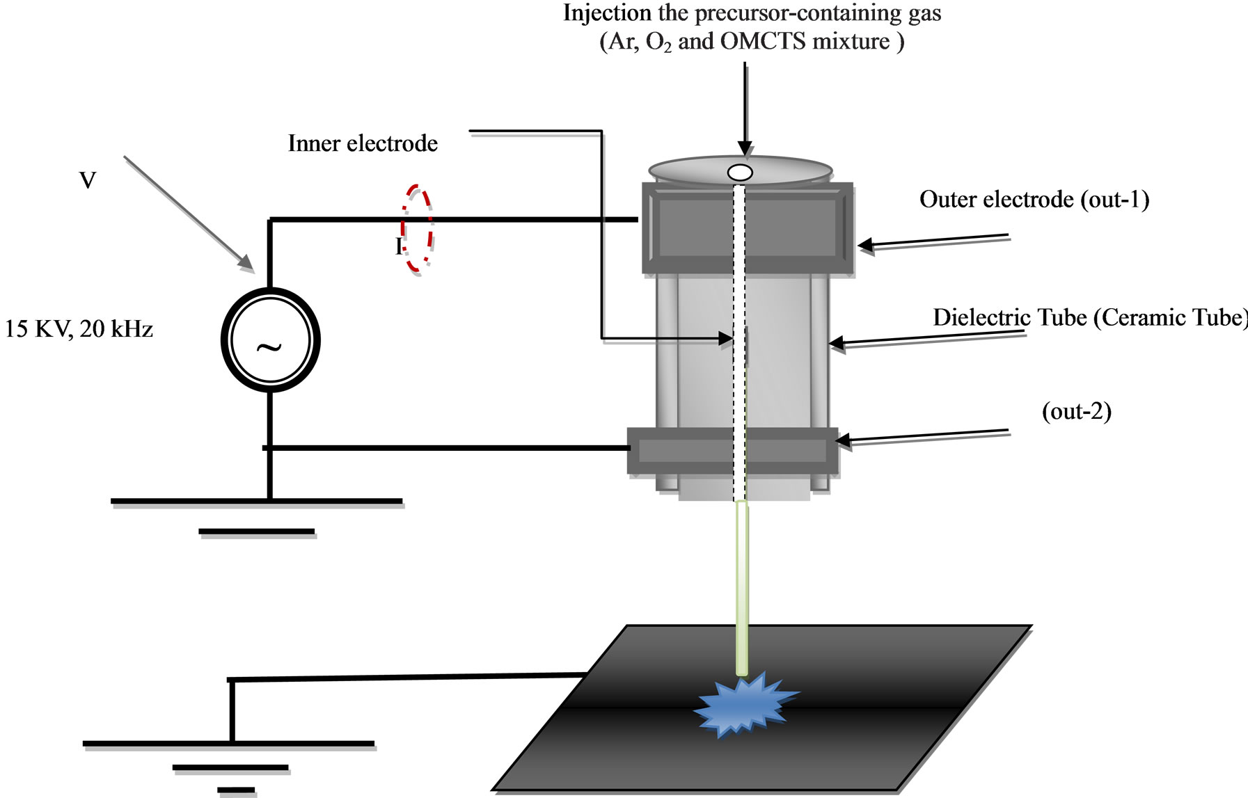
Figure 1. Schematic of discharge system APPJ operated from 3 kV to 15 kV. Frequency 20 kHz; Gas flow rate from 4 L/min to 9 L/min.
3. Results and Discussion
In this study, applied plasma power (expressed as a percentage) was varied from 30% to 100% as illustrated in Figure 2, there was a linear relationship between this power and the voltage probe measurements to maximum applied voltage 15 kV.
At fixed applied voltage 8 kV, the Axial distribution of temperatures from the nozzle to the substrate shown in Figure 3, where maximal temperature of the gas about 49˚C at the end of the nozzle and about 27˚C at the substrate, this mean that the temperature decrease dramatically far away from the jet, i.e. from nozzle to the substrate. Moreover the variation of the temperatures due to flow rate changes for Ar are shown in Figure 4, where as the flow rate was decreased from 4 L/min to 9 L/min, the temperature was decreased from 52˚C to 37˚C at the nozzle and from 29˚C to 25˚C at the substrate. Similar behavior for Ar/O2 mixing but with lower temperature than Argon, Ar plasma had higher gas temperature than the Ar/O2 plasma. This difference between the temperatures of Ar/O2 and Ar plasmas might be attributed due to:
1) Temperature is a strong function of a mixing ratio, the decrement in the electron temperature with a mixing ratio is mainly due to the large inelastic cross section of the mixed gases, the increasing in the sheath length around tip of the jet and the dissociation of the molecular oxygen gas (O2) by argon atoms beside the ionization.
2) Oxygen has higher thermal conductivity (0.0238 W·m−1·K−1) than Ar (0.0162 W·m−1·K−1). Higher thermal conductivity of O2 can transfer and consume thermal energy effectively compared with Ar.
3) Due to oxygen gas (O2), inelastic collisions occur with suitable precursor molecules to produce ions, atoms, and free radicals. A complex mixture of reactive species is produced. Neutral and ionic reactive species strike the Si surface that are in contact with them to form products that are represent coating.
The length and intensity of the plasma jet were considerably influenced by gas flow rate and applied voltage as Figures 5 and 6. Figure 5 shows that the effect of applied voltage on the length of plasma plume in Ar and Ar/O2,
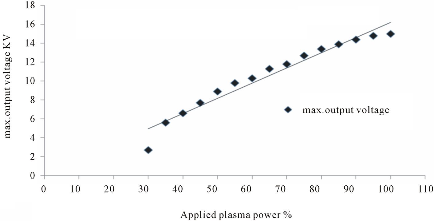
Figure 2. Change in maximum output voltage at varying applied plasma powers.
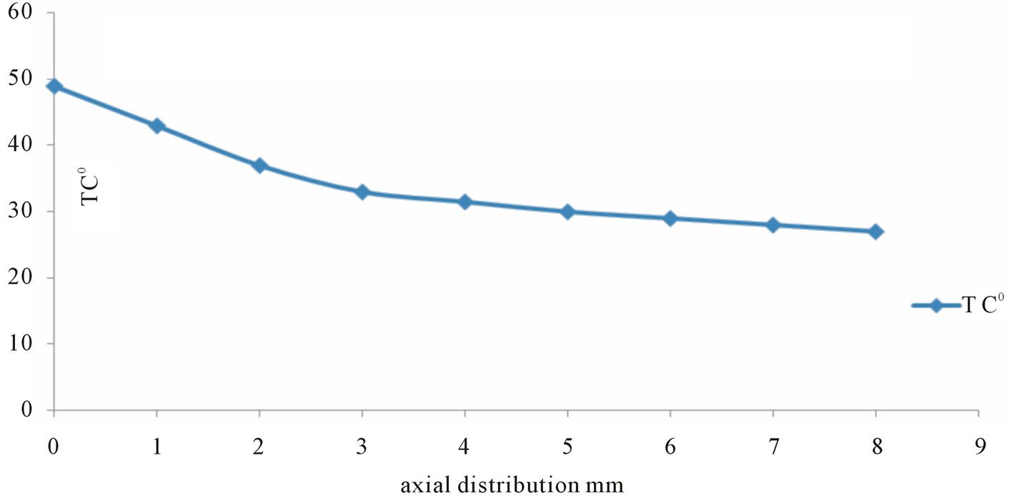
Figure 3. Axial distribution of temperature from the nozzle to the substrate.
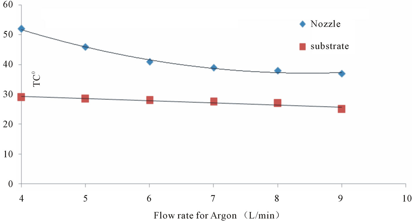
Figure 4. The variation of the temperature due to flow rate changes.
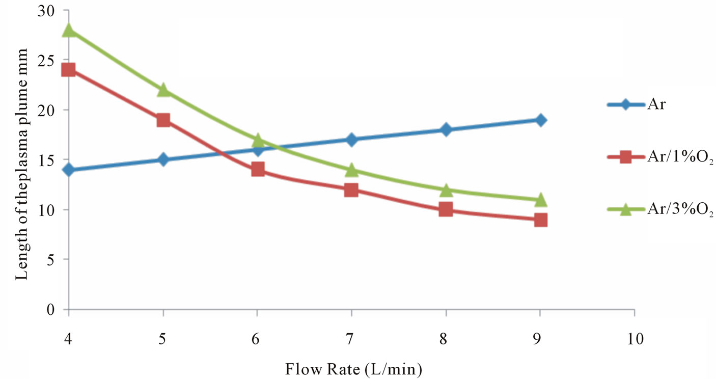
Figure 5. Variation of the plasma plume length due to flow rate changes.
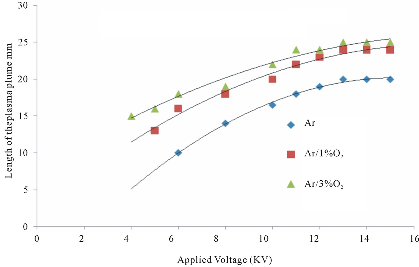
Figure 6. Variation of the plasma plume length due to applied voltage.
where the length of both kinds of plasma jets (Ar and Ar/O2) increases as the applied voltage increases. For Ar, the length of plasma jet was varied within a small range of about 7 mm when the applied voltage was changed from 6 kV to 15 kV. For Ar/O2, the length of plasma jet varied within 10 mm when the applied voltage was changed from 4 kV to 15 kV, for all cases the gas flow rate fixed at 4 L/min for argon.
Figure 6 shows that the length of plasma jet is dependent on the gas flow rate, and an optimum flow rate for producing long plasma jet was to be about 4 L/min and the applied voltage was fixed at 8 kV, where the length of the plasma plume, for argon increase linearly and decrease for Ar/O2 mixtures, as the flow rate increase.
As shown, the length and intensity of plasma jets show dependence on the gas flow rate and the applied voltage. Depending on the gas flow rate, the plasma jets exhibit two modes of operations: laminar and turbulent modes. Laminar mode is formed at low gas flow rate, while turbulent mode is produced as a gas flow rate is increased. The transition from laminar to turbulent mode is closely associated with a noticeable decrease of plasma jet length. The transition from laminar to turbulent mode can be detected by Reynolds number, which can be defined as follows [19-21]:

ρ (kg/m3) is the gas density, D (m) is the hole diameter, μ (N·s/m2) is the gas dynamic viscosity which is related to temperature and pressure, Q (m3/s) is the gas volumetric flow rate, the value of viscosity was selected when the temperature from 20˚C - 25˚C and used basic parameters as shown in Table 1. Furthermore the Reynolds numbers of Ar, Ar/3% O2 and OMCTS were calculated and compared for various gas flow rates as follow in Table 2.
When the Reynolds number is above 2300, laminar mode is gradually progressing to turbulent mode. If the Reynolds number is above 4000, turbulent mode is perfectly developed [21]. The relation of the gas flow and plasma length is vital in the treatment of the Si wafer for coating processes placed on a small distance in industrial applications. The variation of plasma jet length corresponding to the gas flow rate and applied voltage change are shown in Figure 7.
Photos of the substrates after the coating process using APPJ are represented by Figure 8 by the scanning microscope, using (Ar, 3% O2 and OMCTS) concentrations at different flow rates, plasma jet plume is 8 mm in length and 9 kV in applied voltage. Deposition is carried out with the plasma jet pointing perpendicular to the substrate, where the surface remains at room temperature (20˚C - 30˚C), moreover gas over a constant exposure time at 90 sec.
Figure 9 shows that the Coating process increases as adding O2 increases, where the deposition rate increased initially and began to decrease when the flow rate transient from the laminar mode to turbulent mode as the calculated Reynolds number increases, finally the coating process might be attributed due to:
1) Ions are accelerated onto the substrate at high kinetic energy. When the ions strike the surface atoms, momentum transfer takes places, and the atoms are knocked out of the surface and into the gas phase, where they are pumped away [22]. Taking into consideration that the sputtered atoms (from jet, (OMCTS) substrate of the Si wafer, and the polymer of any organic material from the substrate of the wafer) can be recondensed onto a nearby region (substrate) to form a coating, thus sputtering can be used to both etch and deposit or an important
Figure 7. Variation of plasma jet length corresponding to the gas flow rate and applied voltage change.
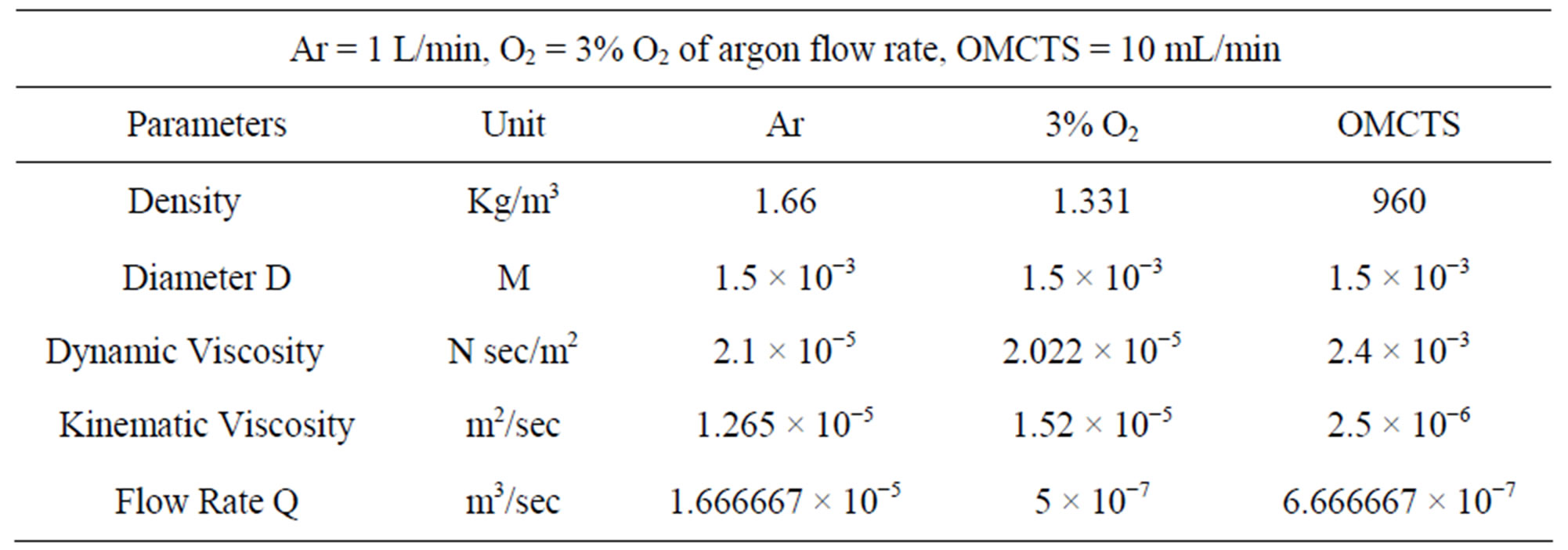
Table 1. List of parameters for Reynolds.
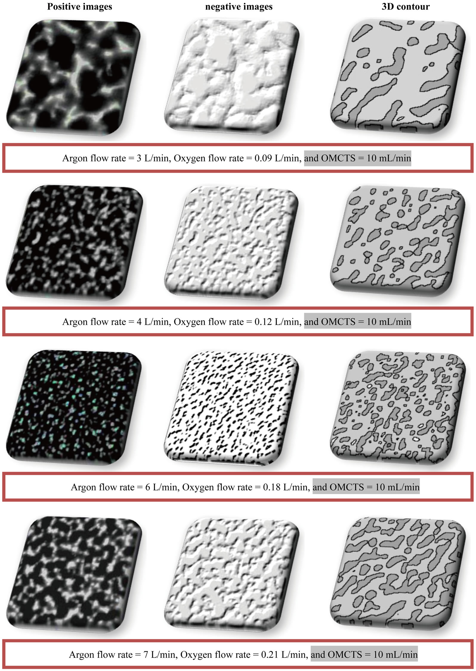
Figure 8. The scanning microscope images of the coating method using APPJ coated Si(100), using (Ar, 3% O2 and OMCTS) at different flow rates.
case for dust plasma effect on the nano-coating process of Si.
2) When the substrate is exposed on gas plasma, the plasma species (ions, electrons, radicals, UV-radiation, neutrons, etc.) interact with substrate chemically and physically. Initially, the gas molecules are dissociated into active species such as ions, electrons, and radicals. The active species would collide with the molecules on substrate surface. UV-radiation and the collisions lead to the radical formation by chain scission of molecules and abstraction taking-off atoms on molecular chain. Free radicals generated in the plasma treatment on polymeric
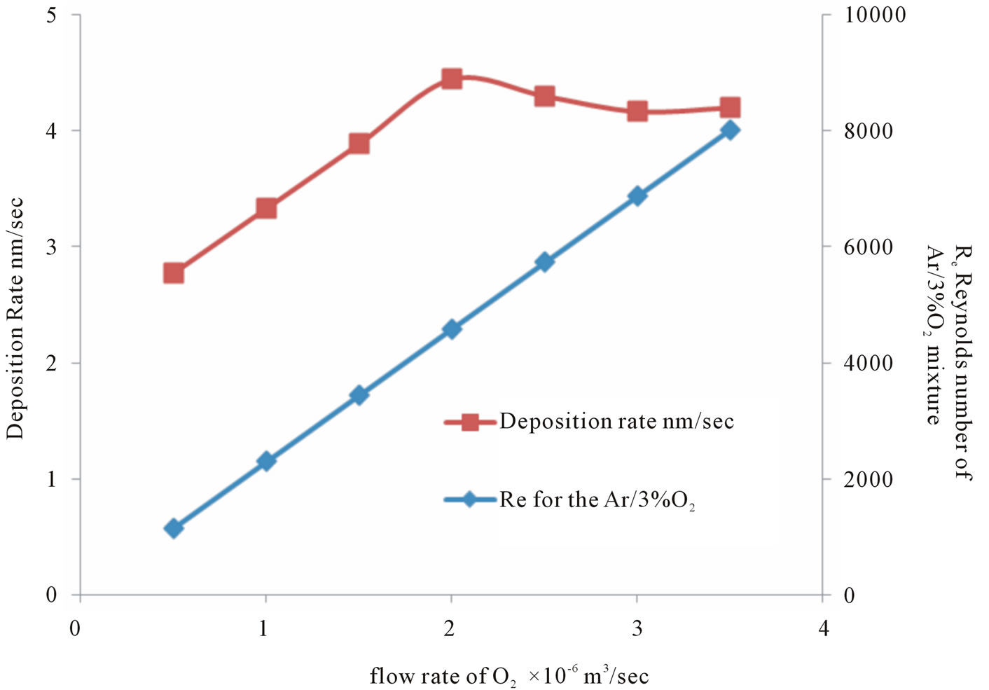
Figure 9. The relation between deposition rate and the calculated Reynolds number with the flow rate of oxygen.
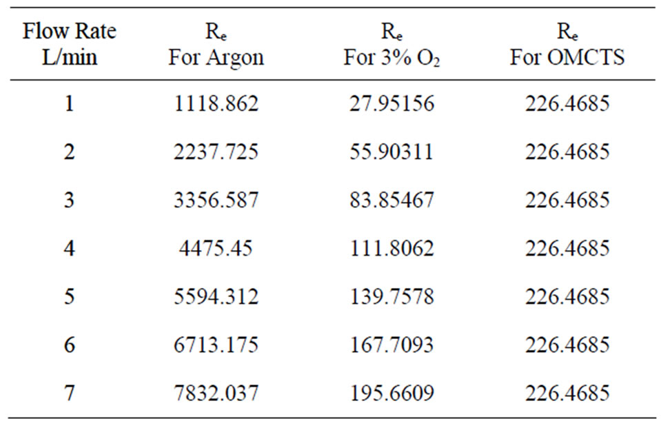
Table 2. Calculated Reynolds numbers.
materials play an important role in surface modification [23,24]. Radical species on plasma would interact with the radicals on substrate molecules, and then new functional groups are generated. Moreover, the chain crosslinking is induced by re-combination between radicals. After plasma treatment on the substrate, unstable free radicals would recombine rapidly with other active species while stable free radicals remain as living radicals. These phenomena would make graft polymerization on substrate surface [25].
4. Conclusions
To avoid substrate damage including increasing plasma density without increasing the kinetic energy of the ion bombardment, there are some few precautions are given here to insure good media for silicon wafer prepared for coating such as:
1) Atmospheric Pressure Plasma Jet (APPJ) for OMCTS (sensitive material for solar cells) coating was used.
2) The good earthed for the Si wafer, which was insulated from the two electrodes.
3) Material OMCTS is suitable for coating process at room temperature.
4) The wafer was negative bias with respect to the plasma jet, then the positive ions sputter with wafer.
5) The best conditions for coating wafer were defined, by measuring maximum applied voltage, the temperately variation of current, the nozzle and the substrate temperature’s, ion velocity, ion density, plasma plume length, and the perfect distance between the nozzle and the substrate.
6) Deposition is carried out with the plasma jet pointing perpendicular to the substrate, where the surface remains at room temperature (20˚C - 30˚C).
7) Plasma jet plume is fixed at 8 mm equal in length of the plasma plume and 9 kV in applied voltage.
8) In the Coating process, as increasing the adding O2, then deposition rate initially was increased and begin to decrease related to the transition from the laminar flow to turbulent flow. The transition from laminar to turbulent modes was observed at a flow rate between 4 and 8 L/min in Ar plasma.
9) A minute amount of Oxygen (3% O2 from argon flow rate) for coating was preferred, to avoid the loss of energy by dissociation and excitation when the ratio of the oxygen increase than 3%.
10) The length and shape of plasma jet in Ar/O2 mixture were influenced by gas flow rate and applied voltage. Ar plasma jet was to be less sensitive to the gas flow rate and the applied voltage.
11) Under the same experimental conditions, Ar plasma had a high plasma jet current and much distorted current waveform compared to Ar/O2 plasma. Ar plasma had more ability to produce active species chemically.
REFERENCES
- U. Lommatzsch, D. Pasedag, A. Baalmann and H.-E. Wagner, “Atmospheric Pressure Plasma Jet Treatment of Polyethylene Surfaces for Adhesion Improvement,” Plasma Processes and Polymers, Vol. 4, Supple. 1, 2007, pp. 1041- 1045. doi:10.1002/ppap.200732402
- C. Huang, S.-Y. Wu, Y.-C. Chang, C.-H. Pan and C.-Y. Tsai, “The Protection of Flexible DSSC Polymeric Substrate using Atmospheric Pressure Plasma Coating Special Issue for the 2009 International Symposium of DyeSensitized Solar Cells,” Journal of the Chinese Chemical Society, Vol. 57, No. 5B, 2010, p. 1208.
- L. Zajickova, J. Janca, and V. Perina, “Characterization of Silicon Oxide Thin Films Deposited by Plasma Enhanced Chemical Vapour Deposition from Octamethylcyclotetrasiloxane/Oxygen Feeds,” Thin Solid Films, Vol. 338, No. 1-2, 1999, pp. 45-59. doi:10.1016/S0040-6090(98)00976-6
- J. Benedikt, K. Focke, A. Yanuas-Gil and A. V. Keudell, “Atmospheric Pressure Microplasma Jet as a Depositing Tool,” Applied Physics Letters, Vol. 89, No. 25, 2006, pp. 251-253. doi:10.1063/1.2423233
- Y. Qi, Z. G. Xiao and T. D. Mantei, “Comparison of Silicon Dioxide Layers Grown from Three Polymethylsiloxane Precursors in a High-Density Oxygen Plasma,” Journal of Vacuum Science & Technology A, Vol. 21, No. 4, 2003, pp. 1064-1068.
- W. Bensch and W. Bergholz, “An FT-IR Study of Silicon Dioxides for VLSI Microelectronics,” Semiconductor Science and Technology, Vol. 5, No. 5, 1990, p. 421. doi:10.1088/0268-1242/5/5/008
- F. Massines, N. Gherardi, A. Fornelli and S. Martin, “Atmospheric Pressure Plasma Deposition of Thin Films by Townsend Dielectric Barrier Discharge,” Surface and Coatings Technology, Vol. 200, No. 5-6, 2005, pp. 1855- 1861. doi:10.1016/j.surfcoat.2005.08.010
- T. P. Kasih, S. Kuroda and H. Kubota, “A Nonequilibrium, Atmospheric-Pressure Argon Plasma Torch for Deposition of Thin Silicon Dioxide Films,” Chemical Vapor Deposition, Vol. 13, No. 4, 2007, pp. 169-175. doi:10.1002/cvde.200606535
- Y. Sawada, S. Ogawa and M. Kogoma, “Synthesis of Plasma-Polymerized Tetraethoxysilane and Hexame-Thyldisiloxane Films Prepared by Atmospheric Pressure Glow Discharge,” Journal of Physics D: Applied Physics, Vol. 28, No. 8, 1995, p. 1661. doi:10.1088/0022-3727/28/8/015
- M. Noborisaka, T. Hirako, A. Shirakura, T. Watanabe, M. Morikawa, M. Seki and T. Suzuki, “Synthesis of DiamondLike Carbon Films on Planar and Non-Planar Geometries by the Atmospheric Pressure Plasma Chemical Vapor Deposition Method,” Japanese Journal of Applied Physics, Vol. 51, No. 9, 2012, Article ID: 090117.
- L. J. Ward, W. C. E. Schofield, J. P. S. Badyal, A. J. Goodwin and P. J. Merlin, “Atmospheric Pressure Glow Discharge Deposition of Polysiloxane and SiOx Film,” Langmuir, Vol. 19, No. 6, 2003, pp. 2110-2114. doi:10.1021/la0204287
- A. Ramamoorthy, M. Rahman, D. A. Mooney, J. M. D. MacElroy and D. P. Dowling, “The Influence of Processes Parameters on Chemistry, Roughness and Morphology of Siloxane Films Deposited by an Atmospheric Plasma Jet System,” Plasma Processes and Polymers, Vol. 6, Suppl. 1, 2009, p. S530. doi:10.1002/ppap.200931109
- D. P. Dowling, A. Ramamoorthy, M. Rahman, D. A. Mooney and J. M. D. MacElroy, “Influence of Atmospheric Plasma Source and Gas Composition on the Properties of Deposited Siloxane Coatings,” Plasma Processes and Polymers, Vol. 6, Supple. 1, 2009, p. S483. doi:10.1002/ppap.200931110
- S. E. Babayan, J. Y. Jeong and R. F. Hicks, “Deposition of Silicon Dioxide Films with an Atmospheric-Pressure Plasma Jet,” Plasma Sources Science and Technology, Vol. 7, No. 3, 1998, p. 286. doi:10.1088/0963-0252/7/3/006
- L. O’Neill, N. Shephard, S. Leadley and J. Adhes, “Atmospheric Pressure Plasma Polymerised Primer to Promote Adhesion of Silicones,” The Journal of Adhesion, Vol. 84, No. 6, 2008, pp. 562-577. doi:10.1080/00218460802161624
- J. Albaugh, C. O’Sullivan and L. O’Neill, “Controlling Deposition Rates in an Atmospheric Pressure Plasma System,” Surface and Coatings Technology, Vol. 203, No. 5-7, 2008, pp. 844-847. doi:10.1016/j.surfcoat.2008.05.047
- G. Guethlein, T. Houck, J. McCarrick and S. Sampayan, “Faraday Cup Measurements of Ions Backstreaming into a Electron Beam Impinging on a Plasma Plume,” Proceedings of Linear Accelerator Conference, Monterey, 21- 25 August 2000, pp. 467-469.
- “Viscosity.” http://en.wikipedia.org/wiki/Viscosity
- F. M. White, “Viscous Fluid Flow,” McGraw-Hill, New York, 1974.
- R. B. Bird, W. E. Stewart and E. N. Lightfoot, “Transport Phenomena,” Wiley, New York, 1960.
- M. Lieberman and A. Lichtenberg, “Principles of Plasma Discharges and Materials Processing,” John Wiley & Sons, New York, 1994.
- M. Shenton, M. Lovell-Hoare and G. Steven, “Adhesion Enhancement of Polymer Surfaces by Atmospheric Plasma Treatment,” Journal of Physics D: Applied Physics, Vol. 34, No. 18, 2001, p. 2754. doi:10.1088/0022-3727/34/18/307
- A. Hollander, R. Wilken and J. Behnisch, “Subsurface Chemistry in the Plasma Treatment of Polymers,” Surface and Coatings Technology, Vol. 116-119, 1999, pp. 788- 791. doi:10.1016/S0257-8972(99)00297-2
- R. Gardri, J. Roth and Z. Chen, “Sterilization and Plasma Processing of Room Temperature Surfaces with a One Atmosphere Uniform Glow Discharge Plasma (OAUGDP),” Surface and Coatings Technology, Vol. 131, No. 1-3, 2000, pp. 528-541. doi:10.1016/S0257-8972(00)00803-3
- S. Herbert, D. Shinozaki and R. Collactott, “Fine-Scale Morphology of Ultraviolet-Ozone Etched Polyethylene,” Journal of Materials Science, Vol. 31, No. 17, 1996, pp. 4655-4661. doi:10.1007/BF00366366